Scientists from Duke University aren’t exactly ‘brewing’ or ‘cooking up’ the inks but they do come close according to a Jan. 3, 2017 news item on ScienceDaily,
By suspending tiny metal nanoparticles in liquids, Duke University scientists are brewing up conductive ink-jet printer “inks” to print inexpensive, customizable circuit patterns on just about any surface.
A Jan. 3, 2017 Duke University news release (also on EurekAlert), which originated the news item, explains why this technique could lead to more accessible printed electronics,
Printed electronics, which are already being used on a wide scale in devices such as the anti-theft radio frequency identification (RFID) tags you might find on the back of new DVDs, currently have one major drawback: for the circuits to work, they first have to be heated to melt all the nanoparticles together into a single conductive wire, making it impossible to print circuits on inexpensive plastics or paper.
A new study by Duke researchers shows that tweaking the shape of the nanoparticles in the ink might just eliminate the need for heat.
By comparing the conductivity of films made from different shapes of silver nanostructures, the researchers found that electrons zip through films made of silver nanowires much easier than films made from other shapes, like nanospheres or microflakes. In fact, electrons flowed so easily through the nanowire films that they could function in printed circuits without the need to melt them all together.
“The nanowires had a 4,000 times higher conductivity than the more commonly used silver nanoparticles that you would find in printed antennas for RFID tags,” said Benjamin Wiley, assistant professor of chemistry at Duke. “So if you use nanowires, then you don’t have to heat the printed circuits up to such high temperature and you can use cheaper plastics or paper.”
“There is really nothing else I can think of besides these silver nanowires that you can just print and it’s simply conductive, without any post-processing,” Wiley added.
These types of printed electronics could have applications far beyond smart packaging; researchers envision using the technology to make solar cells, printed displays, LEDS, touchscreens, amplifiers, batteries and even some implantable bio-electronic devices. The results appeared online Dec. 16 [2016] in ACS Applied Materials and Interfaces.
Silver has become a go-to material for making printed electronics, Wiley said, and a number of studies have recently appeared measuring the conductivity of films with different shapes of silver nanostructures. However, experimental variations make direct comparisons between the shapes difficult, and few reports have linked the conductivity of the films to the total mass of silver used, an important factor when working with a costly material.
“We wanted to eliminate any extra materials from the inks and simply hone in on the amount of silver in the films and the contacts between the nanostructures as the only source of variability,” said Ian Stewart, a recent graduate student in Wiley’s lab and first author on the ACS paper.
Stewart used known recipes to cook up silver nanostructures with different shapes, including nanoparticles, microflakes, and short and long nanowires, and mixed these nanostructures with distilled water to make simple “inks.” He then invented a quick and easy way to make thin films using equipment available in just about any lab — glass slides and double-sided tape.
“We used a hole punch to cut out wells from double-sided tape and stuck these to glass slides,” Stewart said. By adding a precise volume of ink into each tape “well” and then heating the wells — either to relatively low temperature to simply evaporate the water or to higher temperatures to begin melting the structures together — he created a variety of films to test.
The team say they weren’t surprised that the long nanowire films had the highest conductivity. Electrons usually flow easily through individual nanostructures but get stuck when they have to jump from one structure to the next, Wiley explained, and long nanowires greatly reduce the number of times the electrons have to make this “jump”.
But they were surprised at just how drastic the change was. “The resistivity of the long silver nanowire films is several orders of magnitude lower than silver nanoparticles and only 10 times greater than pure silver,” Stewart said.
The team is now experimenting with using aerosol jets to print silver nanowire inks in usable circuits. Wiley says they also want to explore whether silver-coated copper nanowires, which are significantly cheaper to produce than pure silver nanowires, will give the same effect.
Here’s a link to and a citation for the paper,
Effect of Morphology on the Electrical Resistivity of Silver Nanostructure Films by Ian E. Stewart, Myung Jun Kim, and Benjamin J. Wiley. ACS Appl. Mater. Interfaces, Article ASAP
DOI: 10.1021/acsami.6b12289 Publication Date (Web): December 16, 2016Copyright © 2016 American Chemical Society
This paper is behind a paywall but there is an image of the silver nanowires, which is not exactly compensation but is interesting,
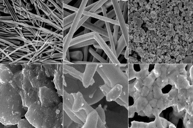
Caption: Duke University chemists have found that silver nanowire films like these conduct electricity well enough to form functioning circuits without applying high temperatures, enabling printable electronics on heat-sensitive materials like paper or plastic.
Credit: Ian Stewart and Benjamin Wiley