Dexter Johnson’s May 16, 2016 posting on his Nanoclast blog (on the IEEE [Institute of Electrical and Electronics Engineers] website) was my first introduction to something wonder-inducing (Note: Links have been removed),
While the growth of 3-D printing has led us to believe we can produce just about any structure with it, the truth is that it still falls somewhat short.
Researchers at Harvard University are looking to realize a more complete range of capabilities for 3-D printing in fabricating both planar and freestanding 3-D structures and do it relatively quickly and on low-cost plastic substrates.
In research published in the journal Proceedings of the National Academy of Sciences (PNAS), the researchers extruded a silver-nanoparticle ink and annealed it with a laser so quickly that the system let them easily “write” free-standing 3-D structures.
While this may sound humdrum, what really takes one’s breath away with this technique is that it can create 3-D structures seemingly suspended in air without any signs of support as though they were drawn there with a pen.
…
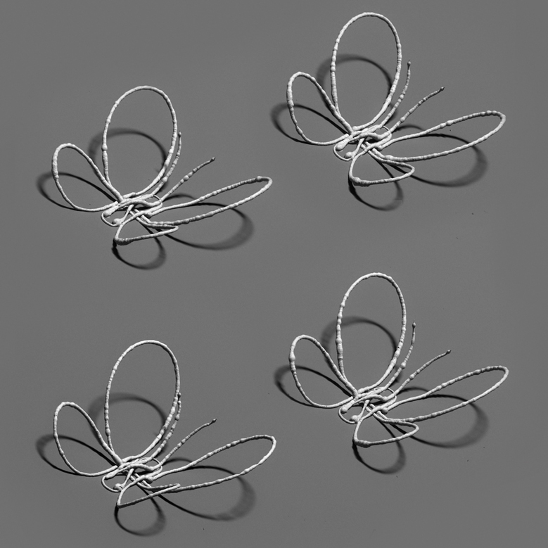
Laser-assisted direct ink writing allowed this delicate 3D butterfly to be printed without any auxiliary support structure (Image courtesy of the Lewis Lab/Harvard University)
A May 16, 2016 Harvard University press release (also on EurekAlert) provides more detail about the work,
“Flat” and “rigid” are terms typically used to describe electronic devices. But the increasing demand for flexible, wearable electronics, sensors, antennas and biomedical devices has led a team at Harvard’s John A. Paulson School of Engineering and Applied Sciences (SEAS) and Wyss Institute for Biologically Inspired Engineering to innovate an eye-popping new way of printing complex metallic architectures – as though they are seemingly suspended in midair.
…
“I am truly excited by this latest advance from our lab, which allows one to 3D print and anneal flexible metal electrodes and complex architectures ‘on-the-fly,’ ” said Lewis [Jennifer Lewis, the Hansjörg Wyss Professor of Biologically Inspired Engineering at SEAS and Wyss Core Faculty member].
Lewis’ team used an ink composed of silver nanoparticles, sending it through a printing nozzle and then annealing it using a precisely programmed laser that applies just the right amount of energy to drive the ink’s solidification. The printing nozzle moves along x, y, and z axes and is combined with a rotary print stage to enable freeform curvature. In this way, tiny hemispherical shapes, spiral motifs, even a butterfly made of silver wires less than the width of a hair can be printed in free space within seconds. The printed wires exhibit excellent electrical conductivity, almost matching that of bulk silver.
When compared to conventional 3D printing techniques used to fabricate conductive metallic features, laser-assisted direct ink writing is not only superior in its ability to produce curvilinear, complex wire patterns in one step, but also in the sense that localized laser heating enables electrically conductive silver wires to be printed directly on low-cost plastic substrates.
According to the study’s first author, Wyss Institute Postdoctoral Fellow Mark Skylar-Scott, Ph.D., the most challenging aspect of honing the technique was optimizing the nozzle-to-laser separation distance.
“If the laser gets too close to the nozzle during printing, heat is conducted upstream which clogs the nozzle with solidified ink,” said Skylar-Scott. “To address this, we devised a heat transfer model to account for temperature distribution along a given silver wire pattern, allowing us to modulate the printing speed and distance between the nozzle and laser to elegantly control the laser annealing process ‘on the fly.’ ”
The result is that the method can produce not only sweeping curves and spirals but also sharp angular turns and directional changes written into thin air with silver inks, opening up near limitless new potential applications in electronic and biomedical devices that rely on customized metallic architectures.
Seeing is believing, eh?
Here’s a link to and a citation for the paper,
Laser-assisted direct ink writing of planar and 3D metal architectures by Mark A. Skylar-Scott, Suman Gunasekaran, and Jennifer A. Lewis. PNAS [Proceedings of the National Academy of Sciences] 2016 doi: 10.1073/pnas.1525131113
I believe this paper is open access.
A question: I wonder what conditions are necessary before you can 3D print something in midair? Much as I’m dying to try this at home, I’m pretty that’s not possible.