Tag Archives: Pulickel Ajayan

Turning asphaltene into graphene

Asphaltene (or asphaltenes are) is waste material that can be turned into graphene according to scientists at Rice University (Texas, US), from a November 18, 2022 news item on ScienceDaily,

Asphaltenes, a byproduct of crude oil production, are a waste material with potential. Rice University scientists are determined to find it by converting the carbon-rich resource into useful graphene.

Muhammad Rahman, an assistant research professor of materials science and nanoengineering, is employing Rice’s unique flash Joule heating process to convert asphaltenes instantly into turbostratic (loosely aligned) graphene and mix it into composites for thermal, anti-corrosion and 3D-printing applications.

The process makes good use of material otherwise burned for reuse as fuel or discarded into tailing ponds and landfills. Using at least some of the world’s reserve of more than 1 trillion barrels of asphaltene as a feedstock for graphene would be good for the environment as well.

A November 17, 2022 Rice University news release (also on EurekAlert), which originated the news item, expands on this exciting news, Note: Links have been removed,

“Asphaltene is a big headache for the oil industry, and I think there will be a lot of interest in this,” said Rahman, who characterized the process as both a scalable and sustainable way to reduce carbon emissions from burning asphaltene.

Rahman is a lead corresponding author of the paper in Science Advances co-led by Rice chemist James Tour, whose lab developed flash Joule heating, materials scientist Pulickel Ajayan and Md Golam Kibria, an assistant professor of chemical and petroleum engineering at the University of Calgary, Canada.

Asphaltenes are 70% to 80% carbon already. The Rice lab combines it with about 20% of carbon black to add conductivity and flashes it with a jolt of electricity, turning it into graphene in less than a second. Other elements in the feedstock, including hydrogen, nitrogen, oxygen and sulfur, are vented away as gases.

“We try to keep the carbon black content as low as possible because we want to maximize the utilization of asphaltene,” Rahman said.

“The government has been putting pressure on the petroleum industries to take care of this,” said Rice graduate student and co-lead author M.A.S.R. Saadi. “There are billions of barrels of asphaltene available, so we began working on this project primarily to see if we could make carbon fiber. That led us to think maybe we should try making graphene with flash Joule heating.”

Assured that Tour’s process worked as well on asphaltene as it did on various other feedstocks, including plastic, electronic waste, tires, coal fly ash and even car parts, the researchers set about making things with their graphene. 

Saadi, who works with Rahman and Ajayan, mixed the graphene into composites, and then into polymer inks bound for 3D printers. “We’ve optimized the ink rheology to show that it is printable,” he said, noting the inks have no more than 10% of graphene mixed in. Mechanical testing of printed objects is forthcoming, he said.

Rice graduate student Paul Advincula, a member of the Tour lab, is co-lead author of the paper. Co-authors are Rice graduate students Md Shajedul Hoque Thakur, Ali Khater, Jacob Beckham and Minghe Lou, undergraduate Aasha Zinke and postdoctoral researcher Soumyabrata Roy; research fellow Shabab Saad, alumnus Ali Shayesteh Zeraati, graduate student Shariful Kibria Nabil and postdoctoral associate Md Abdullah Al Bari of the University of Calgary; graduate student Sravani Bheemasetti and Venkataramana Gadhamshetty, an associate professor, at the South Dakota School of Mines and Technology and its 2D Materials of Biofilm Engineering Science and Technology Center; and research assistant Yiwen Zheng and Aniruddh Vashisth, an assistant professor of mechanical engineering, of the University of Washington.

The research was funded by the Alberta Innovates for Carbon Fiber Grand Challenge programs, the Air Force Office of Scientific Research (FA9550-19-1-0296), the U.S. Army Corps of Engineers (W912HZ-21-2-0050) and the National Science Foundation (1849206, 1920954).  

Here’s a link to and a citation for the paper,

Sustainable valorization of asphaltenes via flash joule heating by M.A.S.R. Saadi, Paul A. Advincula, Md Shajedul Hoque Thakur, Ali Zein Khater, Shabab Saad, Ali Shayesteh Zeraati, Shariful Kibria Nabil, Aasha Zinke, Soumyabrata Roy, Minghe Lou, Sravani N. Bheemasetti, Md Abdullah Al Bari, Yiwen Zheng, Jacob L. Beckham, Venkataramana Gadhamshetty, Aniruddh Vashisth, Md Golam Kibria, James M. Tour, Pulickel M. Ajayan, and Muhammad M. Rahman. Science Advances 18 Nov 2022 Vol 8, Issue 46 DOI: 10.1126/sciadv.add3555

This paper is open access.
3D-printed ‘smart helmets’ for the military

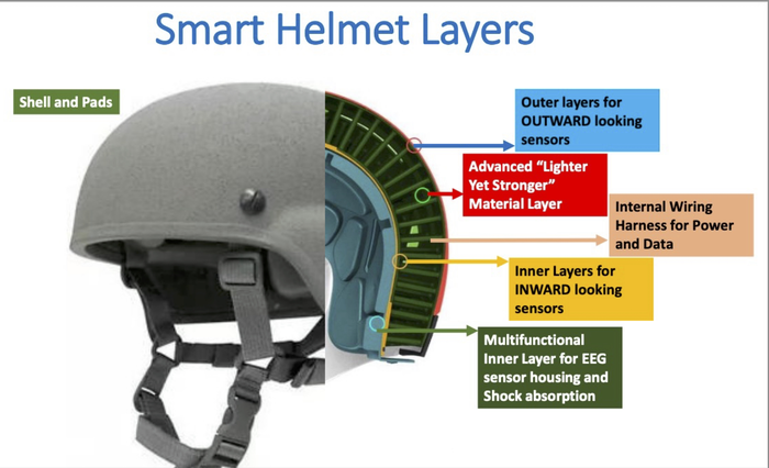
Caption: The Rice University-designed smart helmet is intended to modernize standard-issue military helmets by 3D-printing a nanomaterial-enhanced exoskeleton with embedded sensors to actively protect the brain against kinetic or directed-energy effects. Credit: Rice University

Hopefully this will limit the number of head injuries suffered by soldiers.

Some years ago I was at dinner with friends when one of them, a doctor at the local hospital, told me that the Canadian military, which was in Afghanistan at the time, was dealing with a high number of head injury cases, in part due to the soldiers’ own protective gear.

For example, the protective helmet meant you were less likely to receive a catastrophic injury to your cranium (e.g., metal cracking through bone) but your head would be shaken and that isn’t good for anyone’s brain.

It would seem this project at Rice University (Texas, US) is designed to limit the problem of your own protective gear causing injury, from a November 10, 2021 Rice University news release (also on EurekAlert), Note: Links have been removed,

Rice University researchers have received $1.3 million from the Office of Naval Research through the Defense Research University Instrumentation Program to create the world’s first printable military “smart helmet” using industrial-grade 3D printers. 

Led by principal investigator Paul Cherukuri, executive director of Rice’s Institute of Biosciences and Bioengineering, the Smart Helmet program aims to modernize standard-issue military helmets by 3D-printing a nanomaterial-enhanced exoskeleton with embedded sensors to actively protect the brain against kinetic or directed-energy effects. 

Rice will utilize Carbon Inc.’s L1 printer to develop a strong-but-light military-grade helmet that incorporates advances in materials, image processing, artificial intelligence, haptic feedback and energy storage. The printer enables rapid prototyping that in turn simplifies the process of incorporating the sensors, cameras, batteries and wiring harnesses the program requires, Cherukuri said. 

“Current helmets have evolved little since the last century and are still heavy, bulky, passive devices,” he said. “Because of advances in sensors and additive manufacturing, we’re now reimagining the helmet as a 3D-printed, AI-enabled, ‘always-on’ wearable that detects threats near or far and is capable of launching countermeasures to protect soldiers, sailors, airmen and Marines. Essentially, we’re building J.A.R.V.I.S.”

The Smart Helmet program will use technology drawn from projects like the FlatCam, a system developed by co-investigator and electrical and computer engineer Ashok Veeraraghavan and his colleagues that incorporates sophisticated image processing to eliminate the need for bulky lenses, as well as Cherukuri’s Teslaphoresis, a kind of tractor beam for nanomaterials that could help create physical and electromagnetic shields inside the helmets. 

“A smart helmet task force has been assembled from some of the finest minds at Rice to tackle the challenge of creating a self-contained, intelligent system that protects the warfighter at all times,” Cherukuri said. The task force includes the labs of materials scientist Pulickel Ajayan, civil and environmental engineer and Rice Provost Reginald DesRoches, mechanical engineer Marcia O’Malley, chemist James Tour and Veeraraghavan.

While the location of the L1 has yet to be determined, a Carbon M2 printer will be located at the Oshman Engineering Design Kitchen (OEDK), where it will be available for projects other than the helmet. Rice undergraduates who design and build their mandated capstone projects at the OEDK are taking part in the helmet project, working alongside graduate students and postdoctoral researchers to develop the heads-up display.   

“We’ve got a lot of innovative tech in university labs that has never seen the light of day,” Cherukuri said. “We’re simply developing that technology into a device that gives the men and women protecting our country a real chance at coming home safe and sound. This is for them.”

Flat gallium (gallenene) and nanoelectronics

Another day, another 2D material. A March 9, 2018 news item on ScienceDaily announced the latest thin material from Rice university,

Scientists at Rice University and the Indian Institute of Science, Bangalore, have discovered a method to make atomically flat gallium that shows promise for nanoscale electronics.

The Rice lab of materials scientist Pulickel Ajayan and colleagues in India created two-dimensional gallenene, a thin film of conductive material that is to gallium what graphene is to carbon.

Extracted into a two-dimensional form, the novel material appears to have an affinity for binding with semiconductors like silicon and could make an efficient metal contact in two-dimensional electronic devices, the researchers said.

A March 9, 2018 Rice University news release (also on EurekAlert), which originated the news item, describes the process for creating gallenene,

Gallium is a metal with a low melting point; unlike graphene and many other 2-D structures, it cannot yet be grown with vapor phase deposition methods. Moreover, gallium also has a tendency to oxidize quickly. And while early samples of graphene were removed from graphite with adhesive tape, the bonds between gallium layers are too strong for such a simple approach.

So the Rice team led by co-authors Vidya Kochat, a former postdoctoral researcher at Rice, and Atanu Samanta, a student at the Indian Institute of Science, used heat instead of force.

Rather than a bottom-up approach, the researchers worked their way down from bulk gallium by heating it to 29.7 degrees Celsius (about 85 degrees Fahrenheit), just below the element’s melting point. That was enough to drip gallium onto a glass slide. As a drop cooled just a bit, the researchers pressed a flat piece of silicon dioxide on top to lift just a few flat layers of gallenene.

They successfully exfoliated gallenene onto other substrates, including gallium nitride, gallium arsenide, silicone and nickel. That allowed them to confirm that particular gallenene-substrate combinations have different electronic properties and to suggest that these properties can be tuned for applications.

“The current work utilizes the weak interfaces of solids and liquids to separate thin 2-D sheets of gallium,” said Chandra Sekhar Tiwary, principal investigator on the project he completed at Rice before becoming an assistant professor at the Indian Institute of Technology in Gandhinagar, India. “The same method can be explored for other metals and compounds with low melting points.”

Gallenene’s plasmonic and other properties are being investigated, according to Ajayan. “Near 2-D metals are difficult to extract, since these are mostly high-strength, nonlayered structures, so gallenene is an exception that could bridge the need for metals in the 2-D world,” he said.

Co-authors of the paper are graduate student Yuan Zhang and Associate Research Professor Robert Vajtai of Rice; Anthony Stender, a former Rice postdoctoral researcher and now an assistant professor at Ohio University; Sanjit Bhowmick, Praveena Manimunda and Syed Asif of Bruker Nano Surfaces, Minneapolis; and Rice alumnus Abhishek Singh of the Indian Institute of Science. Ajayan is chair of Rice’s Department of Materials Science and NanoEngineering, the Benjamin M. and Mary Greenwood Anderson Professor in Engineering and a professor of chemistry.

The Air Force Office of Scientific Research sponsored the research, with additional support from the Indo-US Science and Technology Forum, the government of India and a Rice Center for Quantum Materials/Smalley-Curl Postdoctoral Fellowship in Quantum Materials.

Here’s a link to and a citation for the paper,

Atomically thin gallium layers from solid-melt exfoliation by Vidya Kochat, Atanu Samanta, Yuan Zhang, Sanjit Bhowmick, Praveena Manimunda, Syed Asif S. Asif, Anthony S. Stender, Robert Vajtai, Abhishek K. Singh, Chandra S. Tiwary, and Pulickel M. Ajayan. Science Advances 09 Mar 2018: Vol. 4, no. 3, e1701373 DOI: 10.1126/sciadv.1701373

This paper appears to be open access.

Recycle electronic waste by crushing it into nanodust

Given the issues with e-waste this work seems quite exciting. From a March 21, 2017 Rice University news release (also on EurekAlert), Note: Links have been removed,

Researchers at Rice University and the Indian Institute of Science have an idea to simplify electronic waste recycling: Crush it into nanodust.

Specifically, they want to make the particles so small that separating different components is relatively simple compared with processes used to recycle electronic junk now.

Chandra Sekhar Tiwary, a postdoctoral researcher at Rice and a researcher at the Indian Institute of Science in Bangalore, uses a low-temperature cryo-mill to pulverize electronic waste – primarily the chips, other electronic components and polymers that make up printed circuit boards (PCBs) — into particles so small that they do not contaminate each other.

Then they can be sorted and reused, he said.

Circuit boards from electronics, like computer mice, can be crushed into nanodust by a cryo-mill, according to researchers at Rice and the Indian Institute of Science. The dust can then be easily separated into its component elements for recycling.

Circuit boards from electronics, like computer mice, can be crushed into nanodust by a cryo-mill, according to researchers at Rice and the Indian Institute of Science. The dust can then be easily separated into its component elements for recycling. Courtesy of the Ajayan Research Group

The process is the subject of a Materials Today paper by Tiwary, Rice materials scientist Pulickel Ajayan and Indian Institute professors Kamanio Chattopadhyay and D.P. Mahapatra. 

The researchers intend it to replace current processes that involve dumping outdated electronics into landfills, or burning or treating them with chemicals to recover valuable metals and alloys. None are particularly friendly to the environment, Tiwary said.

“In every case, the cycle is one way, and burning or using chemicals takes a lot of energy while still leaving waste,” he said. “We propose a system that breaks all of the components – metals, oxides and polymers – into homogenous powders and makes them easy to reuse.”

The researchers estimate that so-called e-waste will grow by 33 percent over the next four years, and by 2030 will weigh more than a billion tons. Nearly 80 to 85 percent of often-toxic e-waste ends up in an incinerator or a landfill, Tiwary said, and is the fastest-growing waste stream in the United States, according to the Environmental Protection Agency.

The answer may be scaled-up versions of a cryo-mill designed by the Indian team that, rather than heating them, keeps materials at ultra-low temperatures during crushing.

Cold materials are more brittle and easier to pulverize, Tiwary said. “We take advantage of the physics. When you heat things, they are more likely to combine: You can put metals into polymer, oxides into polymers. That’s what high-temperature processing is for, and it makes mixing really easy.

A transparent piece of epoxy, left, compared to epoxy with e-waste reinforcement at right. A cryo-milling process developed at Rice University and the Indian Institute of Science simplifies the process of separating and recycling electronic waste.

A transparent piece of epoxy, left, compared to epoxy with e-waste reinforcement at right. A cryo-milling process developed at Rice University and the Indian Institute of Science simplifies the process of separating and recycling electronic waste. Courtesy of the Ajayan Research Group

“But in low temperatures, they don’t like to mix. The materials’ basic properties – their elastic modulus, thermal conductivity and coefficient of thermal expansion – all change. They allow everything to separate really well,” he said.

The test subjects in this case were computer mice – or at least their PCB innards. The cryo-mill contained argon gas and a single tool-grade steel ball. A steady stream of liquid nitrogen kept the container at 154 kelvins (minus 182 degrees Fahrenheit).

When shaken, the ball smashes the polymer first, then the metals and then the oxides just long enough to separate the materials into a powder, with particles between 20 and 100 nanometers wide. That can take up to three hours, after which the particles are bathed in water to separate them.

“Then they can be reused,” he said. “Nothing is wasted.”

Here’s a link to and a citation for the paper,

Electronic waste recycling via cryo-milling and nanoparticle beneficiation by C.S. Tiwary, S. Kishore, R. Vasireddi, D.R. Mahapatra, P.M. Ajayan, K. Chattopadhyay. Materials Today         http://dx.doi.org/10.1016/j.mattod.2017.01.015 Available online 20 March 2017

This paper is behind a paywall.

A new graphene-based contrast agent for magnetic resonance imaging (MRI)

After teaching a continuing studies course on bioelectronics for Simon Fraser University (Vancouver, Canada), I’ve developed a mild interest in magnetic resonance imaging and contrast agents which this Nov. 11, 2016 news item on phys.org satisfies,

Graphene, the atomically thin sheets of carbon that materials scientists are hoping to use for everything from nanoelectronics and aircraft de-icers to batteries and bone implants, may also find use as contrast agents for magnetic resonance imaging (MRI), according to new research from Rice University.

“They have a lot of advantages compared with conventionally available contrast agents,” Rice researcher Sruthi Radhakrishnan said of the graphene-based quantum dots she has studied for the past two years. “Virtually all of the widely used contrast agents contain toxic metals, but our material has no metal. It’s just carbon, hydrogen, oxygen and fluorine, and in all of our tests so far it has shown no signs of toxicity.”

The initial findings for Rice’s nanoparticles—disks of graphene that are decorated with fluorine atoms and simply organic molecules that make them magnetic—are described in a new paper in the journal Particle and Particle Systems characterization.

A Nov. 10, 2016 Rice University (Texas, US) news release, which originated the news item, describes the work in more detail,

Pulickel Ajayan, the Rice materials scientist who is directing the work, said the fluorinated graphene oxide quantum dots could be particularly useful as MRI contrast agents because they could be targeted to specific kinds of tissues.

“There are tried-and-true methods for attaching biomarkers to carbon nanoparticles, so one could easily envision using these quantum dots to develop tissue-specific contrast agents,” Ajayan said. “For example, this method could be used to selectively target specific types of cancer or brain lesions caused by Alzheimer’s disease. That kind of specificity isn’t available with today’s contrast agents.”

MRI scanners make images of the body’s internal structures using strong magnetic fields and radio waves. As diagnostic tests, MRIs often provide greater detail than X-rays without the harmful radiation, and as a result, MRI usage has risen sharply over the past decade. More than 30 million MRIs are performed annually in the U.S.

Radhakrishnan said her work began in 2014 after Ajayan’s research team found that adding fluorine to either graphite or graphene caused the materials to show up well on MRI scans.

All materials are influenced by magnetic fields, including animal tissues. In MRI scanners, a powerful magnetic field causes individual atoms throughout the body to become magnetically aligned. A pulse of radio energy is used to disrupt this alignment, and the machine measures how long it takes for the atoms in different parts of the body to become realigned. Based on these measures, the scanner can build up a detailed image of the body’s internal structures.

MRI contrast agents shorten the amount of time it takes for tissues to realign and significantly improve the resolution of MRI scans. Almost all commercially available contrast agents are made from toxic metals like gadolinium, iron or manganese.

“We worked with a team from MD Anderson Cancer Center to assess the cytocompatibility of fluorinated graphene oxide quantum dots,” Radhakrishnan said. “We used a test that measures the metabolic activity of cell cultures and detects toxicity as a drop in metabolic activity. We incubated quantum dots in kidney cell cultures for up to three days and found no significant cell death in the cultures, even at the highest concentrations.”

The fluorinated graphene oxide quantum dots Radhakrishnan studies can be made in less than a day, but she spent two years perfecting the recipe for them. She begins with micron-sized sheets of graphene that have been fluorinated and oxidized. When these are added to a solvent and stirred for several hours, they break into smaller pieces. Making the material smaller is not difficult, but the process for making small particles with the appropriate magnetic properties is exacting. Radhakrishnan said there was no “eureka moment” in which she suddenly achieved the right results by stumbling on the best formula. Rather, the project was marked by incremental improvements through dozens of minor alterations.

“It required a lot of optimization,” she said. “The recipe matters a lot.”

Radhakrishnan said she plans to continue studying the material and hopes to eventually have a hand in proving that it is safe and effective for clinical MRI tests.

“I would like to see it applied commercially in clinical ways because it has a lot of advantages compared with conventionally available agents,” she said.

Here’s a link to and a citation for the paper,

Metal-Free Dual Modal Contrast Agents Based on Fluorographene Quantum Dots by Sruthi Radhakrishnan, Atanu Samanta, Parambath M. Sudeep, Kiersten L. Maldonado, Sendurai A. Mani, Ghanashyam Acharya, Chandra Sekhar Tiwary, Abhishek K. Singh, and Pulickel M. Ajayan. Particle & Particle Systems Characterization DOI: 10.1002/ppsc.201600221 Version of Record online: 21 OCT 2016

This paper is behind a paywall.

Graphene in the bone

An international team of US, Brazilian, and Indian scientists has developed a graphene-based material they believe could be used in bone implants. From a Sept. 2, 2016 news item on ScienceDaily,

Flakes of graphene welded together into solid materials may be suitable for bone implants, according to a study led by Rice University scientists.

The Rice lab of materials scientist Pulickel Ajayan and colleagues in Texas, Brazil and India used spark plasma sintering to weld flakes of graphene oxide into porous solids that compare favorably with the mechanical properties and biocompatibility of titanium, a standard bone-replacement material.

A Sept. 2, 2016 Rice University news release (also on EurekAlert), which originated the news item, explains the work in more detail,

The researchers believe their technique will give them the ability to create highly complex shapes out of graphene in minutes using graphite molds, which they believe would be easier to process than specialty metals.

“We started thinking about this for bone implants because graphene is one of the most intriguing materials with many possibilities and it’s generally biocompatible,” said Rice postdoctoral research associate Chandra Sekhar Tiwary, co-lead author of the paper with Dibyendu Chakravarty of the International Advanced Research Center for Powder Metallurgy and New Materials in Hyderabad, India. “Four things are important: its mechanical properties, density, porosity and biocompatibility.”

Tiwary said spark plasma sintering is being used in industry to make complex parts, generally with ceramics. “The technique uses a high pulse current that welds the flakes together instantly. You only need high voltage, not high pressure or temperatures,” he said. The material they made is nearly 50 percent porous, with a density half that of graphite and a quarter of titanium metal. But it has enough compressive strength — 40 megapascals — to qualify it for bone implants, he said. The strength of the bonds between sheets keeps it from disintegrating in water.

The researchers controlled the density of the material by altering the voltage that delivers the highly localized blast of heat that makes the nanoscale welds. Though the experiments were carried out at room temperature, the researchers made graphene solids of various density by raising these sintering temperatures from 200 to 400 degrees Celsius. Samples made at local temperatures of 300 C proved best, Tiwary said. “The nice thing about two-dimensional materials is that they give you a lot of surface area to connect. With graphene, you just need to overcome a small activation barrier to make very strong welds,” he said.

With the help of colleagues at Hysitron in Minnesota, the researchers measured the load-bearing capacity of thin sheets of two- to five-layer bonded graphene by repeatedly stressing them with a picoindenter attached to a scanning electron microscope and found they were stable up to 70 micronewtons. Colleagues at the University of Texas MD Anderson Cancer Center successfully cultured cells on the material to show its biocompatibility. As a bonus, the researchers also discovered the sintering process has the ability to reduce graphene oxide flakes to pure bilayer graphene, which makes them stronger and more stable than graphene monolayers or graphene oxide.

“This example demonstrates the possible use of unconventional materials in conventional technologies,” Ajayan said. “But these transitions can only be made if materials such as 2-D graphene layers can be scalably made into 3-D solids with appropriate density and strength.

“Engineering junctions and strong interfaces between nanoscale building blocks is the biggest challenge in achieving such goals, but in this case, spark plasma sintering seems to be effective in joining graphene sheets to produce strong 3-D solids,” he said.

The researchers have produced an animation depicting of graphene oxide layers being stacked,

A molecular dynamics simulation shows how graphene oxide layers stack when welded by spark plasma sintering. The presence of oxygen molecules at left prevents the graphene layers from bonding, as they do without oxygen at right. Courtesy of the Ajayan and Galvão groups

Here’s a link to and a citation for the paper,

3D Porous Graphene by Low-Temperature Plasma Welding for Bone Implants by Dibyendu Chakravarty, Chandra Sekhar Tiwary, Cristano F. Woellner, Sruthi Radhakrishnan4, Soumya Vinod, Sehmus Ozden, Pedro Alves da Silva Autreto, Sanjit Bhowmick, Syed Asif, Sendurai A Mani, Douglas S. Galvao, and Pulickel M. Ajayan. Advanced Materials DOI: 10.1002/adma.201603146 Version of Record online: 26 AUG 2016

© 2016 WILEY-VCH Verlag GmbH & Co. KGaA, Weinheim

This paper is behind a paywall.

“This is the best microscope we could ever dream of”—Rice University (US) gets new microscope

I believe it’s Emilie Ringe who’s hosting this video about the new microscope at Rice University (Texas, US) and, as you will be able to tell, she’s thrilled.

A June 29, 2015 news item on Nanotechnology Now explains some of Ringe’s excitement,

Rice University, renowned for nanoscale science, has installed microscopes that will allow researchers to peer deeper than ever into the fabric of the universe.

The Titan Themis scanning/transmission electron microscope, one of the most powerful in the United States, will enable scientists from Rice as well as academic and industrial partners to view and analyze materials smaller than a nanometer — a billionth of a meter — with startling clarity.

The microscope has the ability to take images of materials at angstrom-scale (one-tenth of a nanometer) resolution, about the size of a single hydrogen atom.

Images will be captured with a variety of detectors, including X-ray, optical and multiple electron detectors and a 4K-resolution camera, equivalent to the number of pixels in the most modern high-resolution televisions. The microscope gives researchers the ability to create three-dimensional structural reconstructions and carry out electric field mapping of subnanoscale materials.

“Seeing single atoms is exciting, of course, and it’s beautiful,” said Emilie Ringe, a Rice assistant professor of materials science and nanoengineering and of chemistry. “But scientists saw single atoms in the ’90s, and even before. Now, the real breakthrough is that we can identify the composition of those atoms, and do it easily and reliably.” Ringe’s research group will operate the Titan Themis and a companion microscope that will image larger samples.

A June 29, 2015 Rice University news release, which originated the news item, provides more information about electron microscopes, incident electron beams, and the specifics of the second new piece of equipment being installed,

Electron microscopes use beams of electrons rather than rays of light to illuminate objects of interest. Because the wavelength of electrons is so much smaller than that of photons, the microscopes are able to capture images of much smaller things with greater detail than even the highest-resolution optical microscope.

“The beauty of these newer instruments is their analytical capabilities,” Ringe said. “Before, in order to see single atoms, we had to work a machine for an entire day and get it just right and then take a picture and hold our breath. These days, seeing atoms is routine.

“And now we can probe a particular atom’s chemical composition. Through various techniques, either via scattering intensity, X-rays emission or electron-beam absorption, we can figure out, say, that we’re looking at a palladium atom or a carbon atom. We couldn’t do that before.”

Ringe said when an electron beam ejects a bound electron from a target atom, it creates an empty site. “That can be filled by another electron within the atom, and the energy difference between this electron and the missing electron is emitted as an X-ray,” she said. “That X-ray is like a fingerprint, which we can read. Different types of atoms have different energies.”

She said the incident electron beam loses a bit of energy when it knocks an atom’s electron loose, and that energy loss can also be measured with a spectroscope to identify the atom. The X-ray and electron techniques are independent but complementary. “Typically, you use either/or, and it depends on what element you’re looking at,” Ringe said.

The second instrument, a Helios NanoLab 600 DualBeam microscope, will be used for three-dimensional imaging, analysis of larger samples and preparation of thin slices of samples for the more powerful Titan next door.

Both tools reside in the university’s Brockman Hall for Physics, which opened in 2011 and features sophisticated vibration-dampening capabilities. The microscopes require the best possible isolation from vibration, electric fields and acoustic noise to produce the best images, Ringe said.

“We have wanted a high-end microscopy facility at Rice because so many of us are working on nanomaterials,” said Pulickel Ajayan, a professor and founding chair of Rice’s Department of Materials Science and NanoEngineering. “This has been an issue because in order to be competitive you have to have the best atomic-scale characterization techniques. This will put us in business in terms of imaging and understanding new materials.”

He said the facility will position Rice as one of the most competitive institutions to recruit students and faculty, attract grants and publish groundbreaking results.

“A visual image of something on an atomic level can give you so much more information than a few numbers can,” said Peter Rossky, a theoretical chemist and dean of Rice’s Wiess School of Natural Sciences. Comparing images of the same material taken by an older electron microscope and the Titan Themis was like “the difference between a black-and-white TV and high-definition color,” he said.

Ringe said Rice’s Titan is a fourth-generation model manufactured in the Netherlands. It’s the latest and most powerful model and the first to be installed in the United States.

“Taking a complex image — not just a picture but a spectrum image that has lots of energy information — in the older model would take about 35 minutes,” she said. “By that time, the electron beam has destroyed whatever you were trying to look at.

“With this generation, you have the data you need in about two minutes. You can generate a lot more data more quickly. It’s not just better; it’s enabling.”

Edwin Thomas, the William and Stephanie Sick Dean of Rice’s George R. Brown School of Engineering, expects the new instruments to ignite the already strong research culture at the university. “This is going to influence the kind of people who will be attracted to apply to and then come to Rice,” said Thomas, a materials scientist. “I’m sure there will be people on campus who, once they find out the capabilities, are going to shift their compasses and take advantage of these machines. The whole point is to have an impact on science and society.”

Rice plans to host a two-day workshop in September to introduce the microscopes and their capabilities to the research community at the university and beyond. [emphasis mine] Beginning this summer, Ringe said, the electron microscopy center will be open to Rice students and faculty as well as researchers from other universities and industry.

Ringe looks forward to bringing researchers into the new microscopy lab — and to the research that will emerge.

“I hope everyone’s going to come out with a blockbuster paper with images from these instruments,” she said. “I would like every paper from Rice to have fantastic, crystal-clear, atomic-resolution images and the best possible characterization.”

To sum this up, there are two new pieces of equipment (Titan Themis scanning/transmission electron microscope and Helios NanoLab 600 DualBeam microscope) in Rice University’s 2011 facility, Brockman Hall for Physics. They are very excited about having the most powerful microscope in the US (the Titan) and hope to be holding a two-day workshop on these new microscopes for the research community at Rice and at other institutions.

Rice University collaborates with Shandong University on a Joint Center for Carbon Nanomaterials

They’re not billing this as a joint US-China project but with Rice University being in Texas, US and Shandong University being in Shandong (province) in China, I think it’s reasonable to describe it that way. Here’s more about the project from a Feb. 4, 2015 news item on Azonano,

Scientists from Rice University and Shandong University, China, celebrated the opening of the Joint Center for Carbon Nanomaterials, a collaborative facility to study nanotechnology, on Feb. 1 [2015].

Rice faculty members Pulickel Ajayan and Jun Lou, the chair and associate chair, respectively, of the university’s Department of Materials Science and NanoEngineering, took part in the ceremony along with Rice alumnus Lijie Ci, director of the new center and a professor of materials science and engineering at Shandong. The center’s dedication was part of the first International Workshop on Engineering and Applications of Nanocarbon, held Jan. 31-Feb. 2 [2015].

Determining where this new center is located proved to be a challenge. From a Feb. 2, 2015 Rice University news release, which originated the news item,

“We at Rice University are excited and honored to collaborate with Shandong University on this important endeavor,” Rice President David Leebron said in a message recorded for the ceremony. [emphasis mine] “The center represents and combines two very important initiatives for Rice: research excellence and applications in nanosciences and long-term partnerships with the best institutions worldwide.”

“A lot of people are working on carbon nanoscience on both campuses, and we expect they will be interested in taking part,” Ajayan said. “Nanotubes and graphene are essentially the building blocks for the center, but Lijie wants to build ecologically relevant, applied research that can be commercialized. That’s the long-term goal. All of the experience we have had in the area will be beneficial.”

Ajayan expects students from both universities will travel. “People from Rice will be engaged in some of the activities of this joint center, including advising students there. And we hope Shandong students will have the opportunity to come to Rice for a short time,” he said. “The center also contributes to Rice’s goal to build closer connections with China.” [emphases mine]

Ajayan and Ci came to Rice together in 2007 from Rensselaer Polytechnic Institute; Ajayan was a faculty member and Ci was a postdoctoral researcher. At Rice, they introduced the darkest material ever measured at the time of its invention in 2008, an accomplishment that landed them in the Guinness Book of World Records.

They also collaborated on the first two-dimensional material to incorporate graphene and hexagonal boron nitride in a seamless lattice. Such 2-D materials have since become the focus of worldwide research for their potential as electronic components. And Ci, Lou and Ajayan worked together to study the nanoscale friction properties of carbon nanotubes.

I’m inferring from the portions I’ve highlighted that this center is located at Shandong University.

Paint your own battery

Reserchers at Pulickel Ajayan’s laboratory at Rice University have developed a paintable battery (here’s the video),

The June 28, 2012 Rice University news release offers more details about how the paintable battery was achieved,

Lead author [research paper appeared in Nature’s online, open-access journal Scientific Reports] Neelam Singh, a Rice graduate student, and her team spent painstaking hours formulating, mixing and testing paints for each of the five layered components – two current collectors, a cathode, an anode and a polymer separator in the middle.

The materials were airbrushed onto ceramic bathroom tiles, flexible polymers, glass, stainless steel and even a beer stein to see how well they would bond with each substrate.

In the first experiment, nine bathroom tile-based batteries were connected in parallel. One was topped with a solar cell that converted power from a white laboratory light. When fully charged by both the solar panel and house current, the batteries alone powered a set of light-emitting diodes that spelled out “RICE” for six hours; the batteries provided a steady 2.4 volts.

The researchers reported that the hand-painted batteries were remarkably consistent in their capacities, within plus or minus 10 percent of the target. They were also put through 60 charge-discharge cycles with only a very small drop in capacity, Singh said.

You can also find the details and more images at the June 28, 2012 news item on physorg.com,

Each layer is an optimized stew. The first, the positive current collector, is a mixture of purified single-wall carbon nanotubes with carbon black particles dispersed in N-methylpyrrolidone. The second is the cathode, which contains lithium cobalt oxide, carbon and ultrafine graphite (UFG) powder in a binder solution. The third is the polymer separator paint of Kynar Flex resin, PMMA and silicon dioxide dispersed in a solvent mixture. The fourth, the anode, is a mixture of lithium titanium oxide and UFG in a binder, and the final layer is the negative current collector, a commercially available conductive copper paint, diluted with ethanol.

“The hardest part was achieving mechanical stability, and the separator played a critical role,” Singh said. “We found that the nanotube and the cathode layers were sticking very well, but if the separator was not mechanically stable, they would peel off the substrate. Adding PMMA gave the right adhesion to the separator.” Once painted, the tiles and other items were infused with the electrolyte and then heat-sealed and charged.

Singh said the batteries were easily charged with a small solar cell. She foresees the possibility of integrating paintable batteries with recently reported paintable solar cells to create an energy-harvesting combination that would be hard to beat. As good as the hand-painted batteries are, she said, scaling up with modern methods will improve them by leaps and bounds. “Spray painting is already an industrial process, so it would be very easy to incorporate this into industry,” Singh said.

Ajayan’s lab must be a very exciting place to work given the research that has been published in 2012 so far (my Serendipity and coaxial cables post; my Nanosponges clean up spilled oil and release the oil for future use post; my Good heat, bad heat, and cooling oils post).

And to give credit to everyone: co-authors of the paper are graduate students Charudatta Galande and Akshay Mathkar, alumna Wei Gao, now a postdoctoral researcher at Los Alamos National Laboratory, and research scientist Arava Leela Mohana Reddy, all of Rice; Rice Quantum Institute intern Andrea Miranda; and Alexandru Vlad, a former research associate at Rice, now a postdoctoral researcher at the Université Catholique de Louvain, Belgium.

Serendipity and coaxial nanocables

I like the sound of the word coaxial especially when it’s used in conjunction with cable, as in coaxial cable. Adding the world serendipity to the mix, as they did at Rice University, made the June 7, 2012 news item by Jade Boyd on the Nanowerk website irresistible [Note: I have removed a link.],

Thanks to a little serendipity, researchers at Rice University have created a tiny coaxial cable that is about a thousand times smaller than a human hair and has higher capacitance than previously reported microcapacitors.

The nanocable, which is described this week in Nature Communications (“Anomalous high capacitance in a coaxial single nanowire capacitor” [behind paywall]), was produced with techniques pioneered in the nascent graphene research field and could be used to build next-generation energy-storage systems. It could also find use in wiring up components of lab-on-a-chip processors, but its discovery is owed partly to chance.

“We didn’t expect to create this when we started,” said study co-author Jun Lou, associate professor of mechanical engineering and materials science at Rice. “At the outset, we were just curious to see what would happen electrically and mechanically if we took small copper wires known as interconnects and covered them with a thin layer of carbon.”

Boyd’s June 7, 2012 news item can also be read in its entirety at the Rice University website [Note: I have removed some links.],

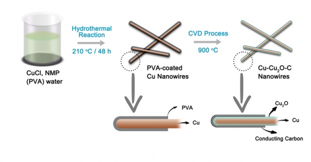
The tiny coaxial cable is remarkably similar in makeup to the ones that carry cable television signals into millions of homes and offices. The heart of the cable is a solid copper wire that is surrounded by a thin sheath of insulating copper oxide. A third layer, another conductor, surrounds that. In the case of TV cables, the third layer is copper again, but in the nanocable it is a thin layer of carbon measuring just a few atoms thick. The coax nanocable is about 100 nanometers, or 100 billionths of a meter, wide.

While the coaxial cable is a mainstay of broadband telecommunications, the three-layer, metal-insulator-metal structure can also be used to build energy-storage devices called capacitors. Unlike batteries, which rely on chemical reactions to both store and supply electricity, capacitors use electrical fields. A capacitor contains two electrical conductors, one negative and the other positive, that are separated by thin layer of insulation. Separating the oppositely charged conductors creates an electrical potential, and that potential increases as the separated charges increase and as the distance between them – occupied by the insulating layer — decreases. The proportion between the charge density and the separating distance is known as capacitance, and it’s the standard measure of efficiency of a capacitor.

The study reports that the capacitance of the nanocable is at least 10 times greater than what would be predicted with classical electrostatics.

“The increase is most likely due to quantum effects that arise because of the small size of the cable,” said study co-author Pulickel Ajayan, Rice’s Benjamin M. and Mary Greenwood Anderson Professor of Mechanical Engineering and Materials Science.

When the project began 18 months ago, Rice postdoctoral researcher Zheng Liu, the lead co-author of the study, intended to make pure copper wires covered with carbon. The techniques for making the wires, which are just a few nanometers wide, are well-established because the wires are often used as “interconnects” in state-of-the-art electronics. Liu used a technique known as chemical vapor deposition (CVD) to cover the wires with a thin coating of carbon. The CVD technique is also used to grow sheets of single-atom-thick carbon called graphene on films of copper.

“When people make graphene, they usually want to study the graphene and they aren’t very interested in the copper,” Lou said. “It’s just used a platform for making the graphene.”

When Liu ran some electronic tests on his first few samples, the results were far from what he expected.

“We eventually found that a thin layer of copper oxide — which is served as a dielectric layer — was forming between the copper and the carbon,” said Liu.

Here’s an image illustrating this process,

The three-layer coaxial nanocable contains a solid copper wire surrounded by a layer of copper oxide that is encased a layer of carbon just a few atoms thick. (Courtesy: Rice University)

The researchers don’t seem to have any particular applications in mind for their nancoaxial cable although they seem hopeful about a few possibilities (from the June 7, 2012 news item on the Rice University website,

The capacitance of the new nanocable is up to 143 microfarads per centimeter squared, better than the best previous results from microcapacitors.

Lou said it may be possible to build a large-scale energy-storage device by arranging millions of the tiny nanocables side by side in large arrays.

“The nanoscale cable might also be used as a transmission line for radio frequency signals at the nanoscale,” Liu said. “This could be useful as a fundamental building block in micro- and nano-sized electromechanical systems like lab-on-a-chip devices.”

Who knows where serendipity will take this discovery?

As for why that word made the item irresistible to me, many years ago I was at a dinner party and one of the guests (a vivid storyteller and born in Sri Lanka) explained the origin of the word, serendipity. Sadly I don’t remember the details of her story, so here’s a less rich version of the story from the Encyclopedia Britannia website,

Serendib, also spelled Serendip, Arabic Sarandīb, name for the island of Sri Lanka (Ceylon). The name, Arabic in origin, was recorded in use at least as early as ad 361 and for a time gained considerable currency in the West. It is best known to speakers of English through the word serendipity, invented in the 18th century by the English man of letters Horace Walpole on the inspiration of a Persian fairy tale, “The Three Princes of Serendip,” whose heroes often made discoveries by chance.