Tag Archives: Rainer Waser

Guide for memristive hardware design

An August 15 ,2022 news item on ScienceDaily announces a type of guide for memristive hardware design,

They are many times faster than flash memory and require significantly less energy: memristive memory cells could revolutionize the energy efficiency of neuromorphic [brainlike] computers. In these computers, which are modeled on the way the human brain works, memristive cells function like artificial synapses. Numerous groups around the world are working on the use of corresponding neuromorphic circuits — but often with a lack of understanding of how they work and with faulty models. Jülich researchers have now summarized the physical principles and models in a comprehensive review article in the renowned journal Advances in Physics.

An August 15, 2022 Forschungszentrum Juelich press release (also on EurekAlert), which originated the news item, describes two papers designed to help researchers better understand and design memristive hardware,

Certain tasks – such as recognizing patterns and language – are performed highly efficiently by a human brain, requiring only about one ten-thousandth of the energy of a conventional, so-called “von Neumann” computer. One of the reasons lies in the structural differences: In a von Neumann architecture, there is a clear separation between memory and processor, which requires constant moving of large amounts of data. This is time and energy consuming – the so-called von Neumann bottleneck. In the brain, the computational operation takes place directly in the data memory and the biological synapses perform the tasks of memory and processor at the same time.

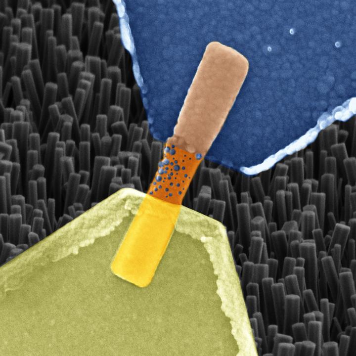
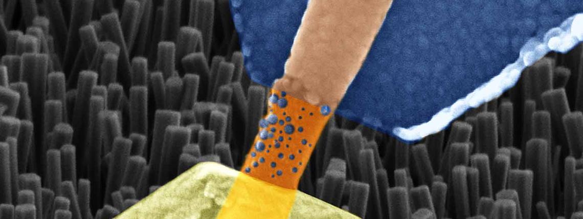
In Jülich, scientists have been working for more than 15 years on special data storage devices and components that can have similar properties to the synapses in the human brain. So-called memristive memory devices, also known as memristors, are considered to be extremely fast, energy-saving and can be miniaturized very well down to the nanometer range. The functioning of memristive cells is based on a very special effect: Their electrical resistance is not constant, but can be changed and reset again by applying an external voltage, theoretically continuously. The change in resistance is controlled by the movement of oxygen ions. If these move out of the semiconducting metal oxide layer, the material becomes more conductive and the electrical resistance drops. This change in resistance can be used to store information.

The processes that can occur in cells are very complex and vary depending on the material system. Three researchers from the Jülich Peter Grünberg Institute – Prof. Regina Dittmann, Dr. Stephan Menzel, and Prof. Rainer Waser – have therefore compiled their research results in a detailed review article, “Nanoionic memristive phenomena in metal oxides: the valence change mechanism”. They explain in detail the various physical and chemical effects in memristors and shed light on the influence of these effects on the switching properties of memristive cells and their reliability.

“If you look at current research activities in the field of neuromorphic memristor circuits, they are often based on empirical approaches to material optimization,” said Rainer Waser, director at the Peter Grünberg Institute. “Our goal with our review article is to give researchers something to work with in order to enable insight-driven material optimization.” The team of authors worked on the approximately 200-page article for ten years and naturally had to keep incorporating advances in knowledge.

“The analogous functioning of memristive cells required for their use as artificial synapses is not the normal case. Usually, there are sudden jumps in resistance, generated by the mutual amplification of ionic motion and Joule heat,” explains Regina Dittmann of the Peter Grünberg Institute. “In our review article, we provide researchers with the necessary understanding of how to change the dynamics of the cells to enable an analog operating mode.”

“You see time and again that groups simulate their memristor circuits with models that don’t take into account high dynamics of the cells at all. These circuits will never work.” said Stephan Menzel, who leads modeling activities at the Peter Grünberg Institute and has developed powerful compact models that are now in the public domain (www.emrl.de/jart.html). “In our review article, we provide the basics that are extremely helpful for a correct use of our compact models.”

Roadmap neuromorphic computing

The “Roadmap of Neuromorphic Computing and Engineering”, which was published in May 2022, shows how neuromorphic computing can help to reduce the enormous energy consumption of IT globally. In it, researchers from the Peter Grünberg Institute (PGI-7), together with leading experts in the field, have compiled the various technological possibilities, computational approaches, learning algorithms and fields of application. 

According to the study, applications in the field of artificial intelligence, such as pattern recognition or speech recognition, are likely to benefit in a special way from the use of neuromorphic hardware. This is because they are based – much more so than classical numerical computing operations – on the shifting of large amounts of data. Memristive cells make it possible to process these gigantic data sets directly in memory without transporting them back and forth between processor and memory. This could reduce the energy efficiency of artificial neural networks by orders of magnitude.

Memristive cells can also be interconnected to form high-density matrices that enable neural networks to learn locally. This so-called edge computing thus shifts computations from the data center to the factory floor, the vehicle, or the home of people in need of care. Thus, monitoring and controlling processes or initiating rescue measures can be done without sending data via a cloud. “This achieves two things at the same time: you save energy, and at the same time, personal data and data relevant to security remain on site,” says Prof. Dittmann, who played a key role in creating the roadmap as editor.

Here’s a link to and a citation for the ‘roadmap’,

2022 roadmap on neuromorphic computing and engineering by Dennis V Christensen, Regina Dittmann, Bernabe Linares-Barranco, Abu Sebastian, Manuel Le Gallo, Andrea Redaelli, Stefan Slesazeck, Thomas Mikolajick, Sabina Spiga, Stephan Menzel, Ilia Valov, Gianluca Milano, Carlo Ricciardi, Shi-Jun Liang, Feng Miao, Mario Lanza, Tyler J Quill, Scott T Keene, Alberto Salleo, Julie Grollier, Danijela Marković, Alice Mizrahi, Peng Yao, J Joshua Yang, Giacomo Indiveri, John Paul Strachan, Suman Datta, Elisa Vianello, Alexandre Valentian, Johannes Feldmann, Xuan Li, Wolfram H P Pernice, Harish Bhaskaran, Steve Furber, Emre Neftci, Franz Scherr, Wolfgang Maass, Srikanth Ramaswamy, Jonathan Tapson, Priyadarshini Panda, Youngeun Kim, Gouhei Tanaka, Simon Thorpe, Chiara Bartolozzi, Thomas A Cleland, Christoph Posch, ShihChii Liu, Gabriella Panuccio, Mufti Mahmud, Arnab Neelim Mazumder, Morteza Hosseini, Tinoosh Mohsenin, Elisa Donati, Silvia Tolu, Roberto Galeazzi, Martin Ejsing Christensen, Sune Holm, Daniele Ielmini and N Pryds. Neuromorphic Computing and Engineering , Volume 2, Number 2 DOI: 10.1088/2634-4386/ac4a83 20 May 2022 • © 2022 The Author(s)

This paper is open access.

Here’s the most recent paper,

Nanoionic memristive phenomena in metal oxides: the valence change mechanism by Regina Dittmann, Stephan Menzel & Rainer Waser. Advances in Physics
Volume 70, 2021 – Issue 2 Pages 155-349 DOI: https://doi.org/10.1080/00018732.2022.2084006 Published online: 06 Aug 2022

This paper is behind a paywall.

Artificial synapse courtesy of nanowires

It looks like a popsicle to me,

Caption: Image captured by an electron microscope of a single nanowire memristor (highlighted in colour to distinguish it from other nanowires in the background image). Blue: silver electrode, orange: nanowire, yellow: platinum electrode. Blue bubbles are dispersed over the nanowire. They are made up of silver ions and form a bridge between the electrodes which increases the resistance. Credit: Forschungszentrum Jülich

Not a popsicle but a representation of a device (memristor) scientists claim mimics a biological nerve cell according to a December 5, 2018 news item on ScienceDaily,

Scientists from Jülich [Germany] together with colleagues from Aachen [Germany] and Turin [Italy] have produced a memristive element made from nanowires that functions in much the same way as a biological nerve cell. The component is able to both save and process information, as well as receive numerous signals in parallel. The resistive switching cell made from oxide crystal nanowires is thus proving to be the ideal candidate for use in building bioinspired “neuromorphic” processors, able to take over the diverse functions of biological synapses and neurons.

A Dec. 5, 2018 Forschungszentrum Jülich press release (also on EurekAlert), which originated the news item, provides more details,

Computers have learned a lot in recent years. Thanks to rapid progress in artificial intelligence they are now able to drive cars, translate texts, defeat world champions at chess, and much more besides. In doing so, one of the greatest challenges lies in the attempt to artificially reproduce the signal processing in the human brain. In neural networks, data are stored and processed to a high degree in parallel. Traditional computers on the other hand rapidly work through tasks in succession and clearly distinguish between the storing and processing of information. As a rule, neural networks can only be simulated in a very cumbersome and inefficient way using conventional hardware.

Systems with neuromorphic chips that imitate the way the human brain works offer significant advantages. Experts in the field describe this type of bioinspired computer as being able to work in a decentralised way, having at its disposal a multitude of processors, which, like neurons in the brain, are connected to each other by networks. If a processor breaks down, another can take over its function. What is more, just like in the brain, where practice leads to improved signal transfer, a bioinspired processor should have the capacity to learn.

“With today’s semiconductor technology, these functions are to some extent already achievable. These systems are however suitable for particular applications and require a lot of space and energy,” says Dr. Ilia Valov from Forschungszentrum Jülich. “Our nanowire devices made from zinc oxide crystals can inherently process and even store information, as well as being extremely small and energy efficient,” explains the researcher from Jülich’s Peter Grünberg Institute.

For years memristive cells have been ascribed the best chances of being capable of taking over the function of neurons and synapses in bioinspired computers. They alter their electrical resistance depending on the intensity and direction of the electric current flowing through them. In contrast to conventional transistors, their last resistance value remains intact even when the electric current is switched off. Memristors are thus fundamentally capable of learning.

In order to create these properties, scientists at Forschungszentrum Jülich and RWTH Aachen University used a single zinc oxide nanowire, produced by their colleagues from the polytechnic university in Turin. Measuring approximately one ten-thousandth of a millimeter in size, this type of nanowire is over a thousand times thinner than a human hair. The resulting memristive component not only takes up a tiny amount of space, but also is able to switch much faster than flash memory.

Nanowires offer promising novel physical properties compared to other solids and are used among other things in the development of new types of solar cells, sensors, batteries and computer chips. Their manufacture is comparatively simple. Nanowires result from the evaporation deposition of specified materials onto a suitable substrate, where they practically grow of their own accord.

In order to create a functioning cell, both ends of the nanowire must be attached to suitable metals, in this case platinum and silver. The metals function as electrodes, and in addition, release ions triggered by an appropriate electric current. The metal ions are able to spread over the surface of the wire and build a bridge to alter its conductivity.

Components made from single nanowires are, however, still too isolated to be of practical use in chips. Consequently, the next step being planned by the Jülich and Turin researchers is to produce and study a memristive element, composed of a larger, relatively easy to generate group of several hundred nanowires offering more exciting functionalities.

The Italians have also written about the work in a December 4, 2018 news item for the Polytecnico di Torino’s inhouse magazine, PoliFlash’. I like the image they’ve used better as it offers a bit more detail and looks less like a popsicle. First, the image,

Courtesy: Polytecnico di Torino

Now, the news item, which includes some historical information about the memristor (Note: There is some repetition and links have been removed),

Emulating and understanding the human brain is one of the most important challenges for modern technology: on the one hand, the ability to artificially reproduce the processing of brain signals is one of the cornerstones for the development of artificial intelligence, while on the other the understanding of the cognitive processes at the base of the human mind is still far away.

And the research published in the prestigious journal Nature Communications by Gianluca Milano and Carlo Ricciardi, PhD student and professor, respectively, of the Applied Science and Technology Department of the Politecnico di Torino, represents a step forward in these directions. In fact, the study entitled “Self-limited single nanowire systems combining all-in-one memristive and neuromorphic functionalities” shows how it is possible to artificially emulate the activity of synapses, i.e. the connections between neurons that regulate the learning processes in our brain, in a single “nanowire” with a diameter thousands of times smaller than that of a hair.

It is a crystalline nanowire that takes the “memristor”, the electronic device able to artificially reproduce the functions of biological synapses, to a more performing level. Thanks to the use of nanotechnologies, which allow the manipulation of matter at the atomic level, it was for the first time possible to combine into one single device the synaptic functions that were individually emulated through specific devices. For this reason, the nanowire allows an extreme miniaturisation of the “memristor”, significantly reducing the complexity and energy consumption of the electronic circuits necessary for the implementation of learning algorithms.

Starting from the theorisation of the “memristor” in 1971 by Prof. Leon Chua – now visiting professor at the Politecnico di Torino, who was conferred an honorary degree by the University in 2015 – this new technology will not only allow smaller and more performing devices to be created for the implementation of increasingly “intelligent” computers, but is also a significant step forward for the emulation and understanding of the functioning of the brain.

“The nanowire memristor – said Carlo Ricciardirepresents a model system for the study of physical and electrochemical phenomena that govern biological synapses at the nanoscale. The work is the result of the collaboration between our research team and the RWTH University of Aachen in Germany, supported by INRiM, the National Institute of Metrological Research, and IIT, the Italian Institute of Technology.”

h.t for the Italian info. to Nanowerk’s Dec. 10, 2018 news item.

Here’s a link to and a citation for the paper,

Self-limited single nanowire systems combining all-in-one memristive and neuromorphic functionalities by Gianluca Milano, Michael Luebben, Zheng Ma, Rafal Dunin-Borkowski, Luca Boarino, Candido F. Pirri, Rainer Waser, Carlo Ricciardi, & Ilia Valov. Nature Communicationsvolume 9, Article number: 5151 (2018) DOI: https://doi.org/10.1038/s41467-018-07330-7 Published: 04 December 2018

This paper is open access.

Just use the search term “memristor” in the blog search engine if you’re curious about the multitudinous number of postings on the topic here.

Memristor shakeup

New discoveries suggest that memristors do not function as was previously theorized. (For anyone who wants a memristor description, there’s this Wikipedia entry.) From an Oct. 13, 2015 posting by Alexander Hellemans for the Nanoclast blog (on the IEEE [Institute for Electrical and Electronics Engineers]), Note: Links have been removed,

What’s going to replace flash? The R&D arms of several companies including Hewlett Packard, Intel, and Samsung think the answer might be memristors (also called resistive RAM, ReRAM, or RRAM). These devices have a chance at unseating the non-volatile memory champion because, they use little energy, are very fast, and retain data without requiring power. However, new research indicates that they don’t work in quite the way we thought they do.

The fundamental mechanism at the heart of how a memristor works is something called an “imperfect point contact,” which was predicted in 1971, long before anybody had built working devices. When voltage is applied to a memristor cell, it reduces the resistance across the device. This change in resistance can be read out by applying another, smaller voltage. By inverting the voltage, the resistance of the device is returned to its initial value, that is, the stored information is erased.

Over the last decade researchers have produced two commercially promising types of memristors: electrochemical metallization memory (ECM) cells, and valence change mechanism memory (VCM) cells.

Now international research teams lead by Ilia Valov at the Peter Grünberg Institute in Jülich, Germany, report in Nature Nanotechnology and Advanced Materials that they have identified new processes that erase many of the differences between EMC and VCM cells.

Valov and coworkers in Germany, Japan, Korea, Greece, and the United States started investigating memristors that had a tantalum oxide electrolyte and an active tantalum electrode. “Our studies show that these two types of switching mechanisms in fact can be bridged, and we don’t have a purely oxygen type of switching as was believed, but that also positive [metal] ions, originating from the active electrode, are mobile,” explains Valov.

Here are links to and citations for both papers,

Graphene-Modified Interface Controls Transition from VCM to ECM Switching Modes in Ta/TaOx Based Memristive Devices by Michael Lübben, Panagiotis Karakolis, Vassilios Ioannou-Sougleridis, Pascal Normand, Pangiotis Dimitrakis, & Ilia Valov. Advanced Materials DOI: 10.1002/adma.201502574 First published: 10 September 2015

Nanoscale cation motion in TaOx, HfOx and TiOx memristive systems by Anja Wedig, Michael Luebben, Deok-Yong Cho, Marco Moors, Katharina Skaja, Vikas Rana, Tsuyoshi Hasegawa, Kiran K. Adepalli, Bilge Yildiz, Rainer Waser, & Ilia Valov. Nature Nanotechnology (2015) doi:10.1038/nnano.2015.221 Published online 28 September 2015

Both papers are behind paywalls.

Memristor, memristor! What is happening? News from the University of Michigan and HP Laboratories

Professor Wei Lu (whose work on memristors has been mentioned here a few times [an April 15, 2010 posting and an April 19, 2012 posting]) has made a discovery about memristors with significant implications (from a June 25, 2014 news item on Azonano),

In work that unmasks some of the magic behind memristors and “resistive random access memory,” or RRAM—cutting-edge computer components that combine logic and memory functions—researchers have shown that the metal particles in memristors don’t stay put as previously thought.

The findings have broad implications for the semiconductor industry and beyond. They show, for the first time, exactly how some memristors remember.

A June 24, 2014 University of Michigan news release, which originated the news item, includes Lu’s perspective on this discovery and more details about it,

“Most people have thought you can’t move metal particles in a solid material,” said Wei Lu, associate professor of electrical and computer engineering at the University of Michigan. “In a liquid and gas, it’s mobile and people understand that, but in a solid we don’t expect this behavior. This is the first time it has been shown.”

Lu, who led the project, and colleagues at U-M and the Electronic Research Centre Jülich in Germany used transmission electron microscopes to watch and record what happens to the atoms in the metal layer of their memristor when they exposed it to an electric field. The metal layer was encased in the dielectric material silicon dioxide, which is commonly used in the semiconductor industry to help route electricity.

They observed the metal atoms becoming charged ions, clustering with up to thousands of others into metal nanoparticles, and then migrating and forming a bridge between the electrodes at the opposite ends of the dielectric material.

They demonstrated this process with several metals, including silver and platinum. And depending on the materials involved and the electric current, the bridge formed in different ways.

The bridge, also called a conducting filament, stays put after the electrical power is turned off in the device. So when researchers turn the power back on, the bridge is there as a smooth pathway for current to travel along. Further, the electric field can be used to change the shape and size of the filament, or break the filament altogether, which in turn regulates the resistance of the device, or how easy current can flow through it.

Computers built with memristors would encode information in these different resistance values, which is in turn based on a different arrangement of conducting filaments.

Memristor researchers like Lu and his colleagues had theorized that the metal atoms in memristors moved, but previous results had yielded different shaped filaments and so they thought they hadn’t nailed down the underlying process.

“We succeeded in resolving the puzzle of apparently contradicting observations and in offering a predictive model accounting for materials and conditions,” said Ilia Valov, principle investigator at the Electronic Materials Research Centre Jülich. “Also the fact that we observed particle movement driven by electrochemical forces within dielectric matrix is in itself a sensation.”

The implications for this work (from the news release),

The results could lead to a new approach to chip design—one that involves using fine-tuned electrical signals to lay out integrated circuits after they’re fabricated. And it could also advance memristor technology, which promises smaller, faster, cheaper chips and computers inspired by biological brains in that they could perform many tasks at the same time.

As is becoming more common these days (from the news release),

Lu is a co-founder of Crossbar Inc., a Santa Clara, Calif.-based startup working to commercialize RRAM. Crossbar has just completed a $25 million Series C funding round.

Here’s a link to and a citation for the paper,

Electrochemical dynamics of nanoscale metallic inclusions in dielectrics by Yuchao Yang, Peng Gao, Linze Li, Xiaoqing Pan, Stefan Tappertzhofen, ShinHyun Choi, Rainer Waser, Ilia Valov, & Wei D. Lu. Nature Communications 5, Article number: 4232 doi:10.1038/ncomms5232 Published 23 June 2014

This paper is behind a paywall.

The other party instrumental in the development and, they hope, the commercialization of memristors is HP (Hewlett Packard) Laboratories (HP Labs). Anyone familiar with this blog will likely know I have frequently covered the topic starting with an essay explaining the basics on my Nanotech Mysteries wiki (or you can check this more extensive and more recently updated entry on Wikipedia) and with subsequent entries here over the years. The most recent entry is a Jan. 9, 2014 posting which featured the then latest information on the HP Labs memristor situation (scroll down about 50% of the way). This new information is more in the nature of a new revelation of details rather than an update on its status. Sebastian Anthony’s June 11, 2014 article for extremetech.com lays out the situation plainly (Note: Links have been removed),

HP, one of the original 800lb Silicon Valley gorillas that has seen much happier days, is staking everything on a brand new computer architecture that it calls… The Machine. Judging by an early report from Bloomberg Businessweek, up to 75% of HP’s once fairly illustrious R&D division — HP Labs – are working on The Machine. As you would expect, details of what will actually make The Machine a unique proposition are hard to come by, but it sounds like HP’s groundbreaking work on memristors (pictured top) and silicon photonics will play a key role.

First things first, we’re probably not talking about a consumer computing architecture here, though it’s possible that technologies commercialized by The Machine will percolate down to desktops and laptops. Basically, HP used to be a huge player in the workstation and server markets, with its own operating system and hardware architecture, much like Sun. Over the last 10 years though, Intel’s x86 architecture has rapidly taken over, to the point where HP (and Dell and IBM) are essentially just OEM resellers of commodity x86 servers. This has driven down enterprise profit margins — and when combined with its huge stake in the diminishing PC market, you can see why HP is rather nervous about the future. The Machine, and IBM’s OpenPower initiative, are both attempts to get out from underneath Intel’s x86 monopoly.

While exact details are hard to come by, it seems The Machine is predicated on the idea that current RAM, storage, and interconnect technology can’t keep up with modern Big Data processing requirements. HP is working on two technologies that could solve both problems: Memristors could replace RAM and long-term flash storage, and silicon photonics could provide faster on- and off-motherboard buses. Memristors essentially combine the benefits of DRAM and flash storage in a single, hyper-fast, super-dense package. Silicon photonics is all about reducing optical transmission and reception to a scale that can be integrated into silicon chips (moving from electrical to optical would allow for much higher data rates and lower power consumption). Both technologies can be built using conventional fabrication techniques.

In a June 11, 2014 article by Ashlee Vance for Bloomberg Business Newsweek, the company’s CTO (Chief Technical Officer), Martin Fink provides new details,

That’s what they’re calling it at HP Labs: “the Machine.” It’s basically a brand-new type of computer architecture that HP’s engineers say will serve as a replacement for today’s designs, with a new operating system, a different type of memory, and superfast data transfer. The company says it will bring the Machine to market within the next few years or fall on its face trying. “We think we have no choice,” says Martin Fink, the chief technology officer and head of HP Labs, who is expected to unveil HP’s plans at a conference Wednesday [June 11, 2014].

In my Jan. 9, 2014 posting there’s a quote from Martin Fink stating that 2018 would be earliest date for the company’s StoreServ arrays to be packed with 100TB Memristor drives (the Machine?). The company later clarified the comment by noting that it’s very difficult to set dates for new technology arrivals.

Vance shares what could be a stirring ‘origins’ story of sorts, provided the Machine is successful,

The Machine started to take shape two years ago, after Fink was named director of HP Labs. Assessing the company’s projects, he says, made it clear that HP was developing the needed components to create a better computing system. Among its research projects: a new form of memory known as memristors; and silicon photonics, the transfer of data inside a computer using light instead of copper wires. And its researchers have worked on operating systems including Windows, Linux, HP-UX, Tru64, and NonStop.

Fink and his colleagues decided to pitch HP Chief Executive Officer Meg Whitman on the idea of assembling all this technology to form the Machine. During a two-hour presentation held a year and a half ago, they laid out how the computer might work, its benefits, and the expectation that about 75 percent of HP Labs personnel would be dedicated to this one project. “At the end, Meg turned to [Chief Financial Officer] Cathie Lesjak and said, ‘Find them more money,’” says John Sontag, the vice president of systems research at HP, who attended the meeting and is in charge of bringing the Machine to life. “People in Labs see this as a once-in-a-lifetime opportunity.”

Here is the memristor making an appearance in Vance’s article,

HP’s bet is the memristor, a nanoscale chip that Labs researchers must build and handle in full anticontamination clean-room suits. At the simplest level, the memristor consists of a grid of wires with a stack of thin layers of materials such as tantalum oxide at each intersection. When a current is applied to the wires, the materials’ resistance is altered, and this state can hold after the current is removed. At that point, the device is essentially remembering 1s or 0s depending on which state it is in, multiplying its storage capacity. HP can build these chips with traditional semiconductor equipment and expects to be able to pack unprecedented amounts of memory—enough to store huge databases of pictures, files, and data—into a computer.

New memory and networking technology requires a new operating system. Most applications written in the past 50 years have been taught to wait for data, assuming that the memory systems feeding the main computers chips are slow. Fink has assigned one team to develop the open-source Machine OS, which will assume the availability of a high-speed, constant memory store. …

Peter Bright in his June 11, 2014 article for Ars Technica opens his article with a controversial statement (Note: Links have been removed),

In 2008, scientists at HP invented a fourth fundamental component to join the resistor, capacitor, and inductor: the memristor. [emphasis mine] Theorized back in 1971, memristors showed promise in computing as they can be used to both build logic gates, the building blocks of processors, and also act as long-term storage.

Whether or not the memristor is a fourth fundamental component has been a matter of some debate as you can see in this Memristor entry (section on Memristor definition and criticism) on Wikipedia.

Bright goes on to provide a 2016 delivery date for some type of memristor-based product and additional technical insight about the Machine,

… By 2016, the company plans to have memristor-based DIMMs, which will combine the high storage densities of hard disks with the high performance of traditional DRAM.

John Sontag, vice president of HP Systems Research, said that The Machine would use “electrons for processing, photons for communication, and ions for storage.” The electrons are found in conventional silicon processors, and the ions are found in the memristors. The photons are because the company wants to use optical interconnects in the system, built using silicon photonics technology. With silicon photonics, photons are generated on, and travel through, “circuits” etched onto silicon chips, enabling conventional chip manufacturing to construct optical parts. This allows the parts of the system using photons to be tightly integrated with the parts using electrons.

The memristor story has proved to be even more fascinating than I thought in 2008 and I was already as fascinated as could be, or so I thought.

Extending memristive theory

This is kind of fascinating. A German research team based at JARA (Jülich Aachen Research Alliance) is suggesting that memristive theory be extended beyond passive components in their paper about Resistive Memory Cells (ReRAM) which was recently published in Nature Communications. From the Apr. 26, 2013 news item on Azonano,

Resistive memory cells (ReRAM) are regarded as a promising solution for future generations of computer memories. They will dramatically reduce the energy consumption of modern IT systems while significantly increasing their performance.

Unlike the building blocks of conventional hard disk drives and memories, these novel memory cells are not purely passive components but must be regarded as tiny batteries. This has been demonstrated by researchers of Jülich Aachen Research Alliance (JARA), whose findings have now been published in the prestigious journal Nature Communications. The new finding radically revises the current theory and opens up possibilities for further applications. The research group has already filed a patent application for their first idea on how to improve data readout with the aid of battery voltage.

The Apr. 23, 2013 JARA news release, which originated the news item, provides some background information about data memory before going on to discuss the ReRAMs,

Conventional data memory works on the basis of electrons that are moved around and stored. However, even by atomic standards, electrons are extremely small. It is very difficult to control them, for example by means of relatively thick insulator walls, so that information will not be lost over time. This does not only limit storage density, it also costs a great deal of energy. For this reason, researchers are working feverishly all over the world on nanoelectronic components that make use of ions, i.e. charged atoms, for storing data. Ions are some thousands of times heavier that electrons and are therefore much easier to ‘hold down’. In this way, the individual storage elements can almost be reduced to atomic dimensions, which enormously improves the storage density.

Here’s how the ions behave in ReRAMs (from the news release),

In resistive switching memory cells (ReRAMs), ions behave on the nanometre scale in a similar manner to a battery. The cells have two electrodes, for example made of silver and platinum, at which the ions dissolve and then precipitate again. This changes the electrical resistance, which can be exploited for data storage. Furthermore, the reduction and oxidation processes also have another effect. They generate electric voltage. ReRAM cells are therefore not purely passive systems – they are also active electrochemical components. Consequently, they can be regarded as tiny batteries whose properties provide the key to the correct modelling and development of future data storage.

In complex experiments, the scientists from Forschungszentrum Jülich and RWTH Aachen University determined the battery voltage of typical representatives of ReRAM cells and compared them with theoretical values. This comparison revealed other properties (such as ionic resistance) that were previously neither known nor accessible. “Looking back, the presence of a battery voltage in ReRAMs is self-evident. But during the nine-month review process of the paper now published we had to do a lot of persuading, since the battery voltage in ReRAM cells can have three different basic causes, and the assignment of the correct cause is anything but trivial,” says Dr. Ilia Valov, the electrochemist in Prof. Rainer Waser’s research group.

This discovery could lead to optimizing ReRAMs and exploiting them in new applications (from the news release),

“The new findings will help to solve a central puzzle of international ReRAM research,” says Prof. Rainer Waser, deputy spokesman of the collaborative research centre SFB 917 ‘Nanoswitches’ established in 2011. In recent years, these puzzling aspects include unexplained long-term drift phenomena or systematic parameter deviations, which had been attributed to fabrication methods. “In the light of this new knowledge, it is possible to specifically optimize the design of the ReRAM cells, and it may be possible to discover new ways of exploiting the cells’ battery voltage for completely new applications, which were previously beyond the reach of technical possibilities,” adds Waser, whose group has been collaborating for years with companies such as Intel and Samsung Electronics in the field of ReRAM elements.

The part I found most interesting, given my interest in memristors, is this bit about extending the memristor theory, from the news release,

The new finding is of central significance, in particular, for the theoretical description of the memory components. To date, ReRAM cells have been described with the aid of the concept of memristors – a portmanteau word composed of “memory” and “resistor”. The theoretical concept of memristors can be traced back to Leon Chua in the 1970s. It was first applied to ReRAM cells by the IT company Hewlett-Packard in 2008. It aims at the permanent storage of information by changing the electrical resistance. The memristor theory leads to an important restriction. It is limited to passive components. “The demonstrated internal battery voltage of ReRAM elements clearly violates the mathematical construct of the memristor theory. This theory must be expanded to a whole new theory – to properly describe the ReRAM elements,” says Dr. Eike Linn, the specialist for circuit concepts in the group of authors. [emphases mine] This also places the development of all micro- and nanoelectronic chips on a completely new footing.

Here’s a link to and a citation for the paper,

Nanobatteries in redox-based resistive switches require extension of memristor theory by I. Valov,  E. Linn, S. Tappertzhofen,  S. Schmelzer,  J. van den Hurk,  F. Lentz,  & R. Waser. Nature Communications 4, Article number: 1771 doi:10.1038/ncomms2784 Published 23 April 2013

This paper is open access (as of this writing).

Here’s a list of my 2013 postings on memristors and memristive devices,

2.5M Euros for Ireland’s John Boland and his memristive nanowires (Apr. 4, 2013 posting)

How to use a memristor to create an artificial brain (Feb. 26, 2013 posting)

CeNSE (Central Nervous System of the Earth) and billions of tiny sensors from HP plus a memristor update (Feb. 7, 2013 posting)

For anyone who cares to search the blog, there are several more.