Tag Archives: scanning probe microscopy

Getting a more complete picture of aerosol particles at the nanoscale

What is in the air we breathe? In addition to the gases we learned about in school there are particles, not just the dust particles you can see, but micro- and nanoparticles too and scientists would like to know more about them.

An August 23, 2017 news item on Nanowerk features work which may help scientists in their quest,

They may be tiny and invisible, says Xiaoji Xu, but the aerosol particles suspended in gases play a role in cloud formation and environmental pollution and can be detrimental to human health.

Aerosol particles, which are found in haze, dust and vehicle exhaust, measure in the microns. One micron is one-millionth of a meter; a thin human hair is about 30 microns thick.

The particles, says Xu, are among the many materials whose chemical and mechanical properties cannot be fully measured until scientists develop a better method of studying materials at the microscale as well as the much smaller nanoscale (1 nm is one-billionth of a meter).

Xu, an assistant professor of chemistry, has developed such a method and utilized it to perform noninvasive chemical imaging of a variety of materials, as well as mechanical mapping with a spatial resolution of 10 nanometers.

The technique, called peak force infrared (PFIR) microscopy, combines spectroscopy and scanning probe microscopy. In addition to shedding light on aerosol particles, Xu says, PFIR will help scientists study micro- and nanoscale phenomena in a variety of inhomogeneous materials.

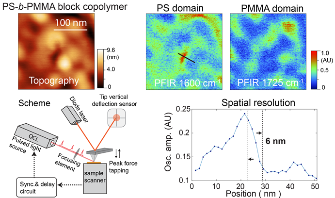
The lower portion of this image by Xiaoji Xu’s group shows the operational scheme of peak force infrared (PFIR) microscopy. The upper portion shows the topography of nanoscale PS-b-PMMA polymer islands on a gold substrate. (Image courtesy of Xiaoji Xu)

An August 22, 2017 Lehih University news release by Kurt Pfitzer (also on EurekAlert), which originated the news item, explains the research in more detail (Note: A link has been removed),

“Materials in nature are rarely homogeneous,” says Xu. “Functional polymer materials often consist of nanoscale domains that have specific tasks. Cellular membranes are embedded with proteins that are nanometers in size. Nanoscale defects of materials exist that affect their mechanical and chemical properties.

“PFIR microscopy represents a fundamental breakthrough that will enable multiple innovations in areas ranging from the study of aerosol particles to the investigation of heterogeneous and biological materials,” says Xu.

Xu and his group recently reported their results in an article titled “Nanoscale simultaneous chemical and mechanical imaging via peak force infrared microscopy.” The article was published in Science Advances, a journal of the American Association for the Advancement of Science, which also publishes Science magazine.

The article’s lead author is Le Wang, a Ph.D. student at Lehigh. Coauthors include Xu and Lehigh Ph.D. students Haomin Wang and Devon S. Jakob, as well as Martin Wagner of Bruker Nano in Santa Barbara, Calif., and Yong Yan of the New Jersey Institute of Technology.

“PFIR microscopy enables reliable chemical imaging, the collection of broadband spectra, and simultaneous mechanical mapping in one simple setup with a spatial resolution of ~10 nm,” the group wrote.

“We have investigated three types of representative materials, namely, soft polymers, perovskite crystals and boron nitride nanotubes, all of which provide a strong PFIR resonance for unambiguous nanochemical identification. Many other materials should be suited as well for the multimodal characterization that PFIR microscopy has to offer.

“In summary, PFIR microscopy will provide a powerful analytical tool for explorations at the nanoscale across wide disciplines.”

Xu and Le Wang also published a recent article about the use of PFIR to study aerosols. Titled “Nanoscale spectroscopic and mechanical characterization of individual aerosol particles using peak force infrared microscopy,” the article appeared in an “Emerging Investigators” issue of Chemical Communications, a journal of the Royal Society of Chemistry. Xu was featured as one of the emerging investigators in the issue. The article was coauthored with researchers from the University of Macau and the City University of Hong Kong, both in China.

PFIR simultaneously obtains chemical and mechanical information, says Xu. It enables researchers to analyze a material at various places, and to determine its chemical compositions and mechanical properties at each of these places, at the nanoscale.

“A material is not often homogeneous,” says Xu. “Its mechanical properties can vary from one region to another. Biological systems such as cell walls are inhomogeneous, and so are materials with defects. The features of a cell wall measure about 100 nanometers in size, placing them well within range of PFIR and its capabilities.”

PFIR has several advantages over scanning near-field optical microscopy (SNOM), the current method of measuring material properties, says Xu. First, PFIR obtains a fuller infrared spectrum and a sharper image—6-nm spatial resolution—of a wider variety of materials than does SNOM. SNOM works well with inorganic materials, but does not obtain as strong an infrared signal as the Lehigh technique does from softer materials such as polymers or biological materials.

“Our technique is more robust,” says Xu. “It works better with soft materials, chemical as well as biological.”

The second advantage of PFIR is that it can perform what Xu calls point spectroscopy.

“If there is something of interest chemically on a surface,” Xu says, “I put an AFM [atomic force microscopy] probe to that location to measure the peak-force infrared response.

“It is very difficult to obtain these spectra with current scattering-type scanning near-field optical microscopy. It can be done, but it requires very expensive light sources. Our method uses a narrow-band infrared laser and costs about $100,000. The existing method uses a broadband light source and costs about $300,000.”

A third advantage, says Xu, is that PFIR obtains a mechanical as well as a chemical response from a material.

“No other spectroscopy method can do this,” says Xu. “Is a material rigid or soft? Is it inhomogeneous—is it soft in one area and rigid in another? How does the composition vary from the soft to the rigid areas? A material can be relatively rigid and have one type of chemical composition in one area, and be relatively soft with another type of composition in another area.

“Our method simultaneously obtains chemical and mechanical information. It will be useful for analyzing a material at various places and determining its compositions and mechanical properties at each of these places, at the nanoscale.”

A fourth advantage of PFIR is its size, says Xu.

“We use a table-top laser to get infrared spectra. Ours is a very compact light source, as opposed to the much larger sizes of competing light sources. Our laser is responsible for gathering information concerning chemical composition. We get mechanical information from the AFM [atomic force microscope]. We integrate the two types of measurements into one device to simultaneously obtain two channels of information.”

Although PFIR does not work with liquid samples, says Xu, it can measure the properties of dried biological samples, including cell walls and protein aggregates, achieving a 10-nm spatial resolution without staining or genetic modification.

This looks like very exciting work.

Here are links and citations for both studies mentioned in the news release (the most recently published being cited first),

Nanoscale simultaneous chemical and mechanical imaging via peak force infrared microscopy by Le Wang, Haomin Wang, Martin Wagner, Yong Yan, Devon S. Jakob, and Xiaoji G. Xu. Science Advances 23 Jun 2017: Vol. 3, no. 6, e1700255 DOI: 10.1126/sciadv.1700255

Nanoscale spectroscopic and mechanical characterization of individual aerosol particles using peak force infrared microscopy by Le Wang, Dandan Huang, Chak K. Chan, Yong Jie Li, and Xiaoji G. Xu. Chem. Commun., 2017,53, 7397-7400 DOI: 10.1039/C7CC02301D First published on 16 Jun 2017

The June 23, 2017 paper is open access while the June 16, 2017 paper is behind a paywall.

Canada’s Spectra Research gets exclusive distribution rights for super duper Asylum research microscopes

It’s all about microscopes, scanning probe and atomic force microscopes, that is. Asylum Research, a US company that recently (May 29, 2012)  announced the world’s first five year instrument warranty for atomic force microscopes, has appointed Canada’s Spectra Research Corporation as an exclusive distributor for Asylum’s microscopy products (and their other scientific instrumentation). From the June 6, 2012 news item on Nanowerk,

As part of its ongoing expansion, Asylum Research, the technology leader in scanning probe and atomic force microscopy (SPM/AFM), announced today that it has appointed Spectra Research Corporation (SRC) as its exclusive distributor in Canada. SRC has served nanotechnology and surface science markets in Canada since 1993. …

“We are very excited about adding Spectra Research to our family of world-wide distributors,” said John Green, Executive Vice President of Sales for Asylum Research. “Their extensive experience in AFM, materials and life science, and scientific instrumentation, will be a great asset to Asylum Research and our ability to help prospective customers make informed decisions.”

Paul Greenwood, President of SRC, added, “… This addition is a good fit with our focus on Canadian markets that include nanotech, surface science and materials characterization”.

SRC, located in Mississauga, Ontario, is one of the Allan Crawford Associates (ACA) group of companies. Neither SRC nor ACA offer much informaton about themselves or products on their websites. As for Asylum Research, you can find this on their About page,

Asylum Research is the technology leader in atomic force and scanning probe microscopy (AFM/SPM) for both materials and bioscience applications.  Founded in 1999, we are an employee owned company dedicated to innovative instrumentation for nanoscience and nanotechnology, with over 250 years combined AFM/SPM experience among our staff. Our instruments are used for a variety of nanoscience applications in material science, physics, polymers, chemistry, biomaterials, and bioscience, including single molecule mechanical experiments on DNA, protein unfolding and polymer elasticity, as well as force measurements for biomaterials, chemical sensing, polymers, colloidal forces, adhesion, and more.
Asylum’s MFP-3D set the standard for AFM technology, with unprecedented precision and flexibility. The MFP-3D is the first AFM with true independent piezo positioning in all three axes, combined with low noise closed-loop feedback sensor technology. The MFP-3D offers both top and bottom sample viewing and easy integration with most commercially-available inverted optical microscopes.

Asylum’s new Cypher AFM sets the new standard as the world’s fastest and highest resolution AFM.  Cypher provides low-drift closed loop atomic resolution for the most accurate images and measurements possible today, point defect atomic resolution, >20X faster AC imaging with small cantilevers, Spot-On™ automated laser and photodetector alignment for easy setup, integrated thermal, acoustic and vibration control, and broad support for all major AFM/SPM scanning modes and capabilities.

Asylum Research offers the lowest cost of ownership of any AFM company. Ask us about our industry-best 5-year warranty, our legendary product and applications support, and our exclusive 6-month money-back satisfaction guarantee. We are dedicated to providing the most technically advanced AFMs for researchers who want to take their experiments to the next level.

There’s a lot more information about their products and services on Asylum Research’s website.

RUSNANO sells an investment based on IRR (internal rate of return)

This is a turnaround. The news items usually state that RUSNANO (Russian Corporation of Nanotechnologies) is about to invest money but this time they’re selling their investment. From the May 28, 2012 news item on Nanowerk,

RUSNANO’s Board of Directors has approved the company’s first exit from a previously-invested company. RUSNANO sells its 27.6 percent equity stake in Advanced Technologies Center, a leading producer of scanning probe microscopes and atomic scales. The sale to the project applicant, NPP CPT will generate IRR of 29.5 percent on RUSNANO’s investment.

RUSNANO’s co-financing enabled the high-tech company founded by Moscow State University professor Igor Yaminsky to reach next level of business and to expand its line of scanning probe microscopes [SPM] and SPM software. RUSNANO has invested 50 million rubles in the project, out of the 140 million rubles originally planned. In December 2011 the portfolio company opened a production site which will double its production capacity up to the revenue levels of 70 million rubles by the end of 2012.

The deal meets two essential RUSNANO’s criteria for successful exit: IRR is no lower than was planned, and the project is able to develop independently.

I had to look up ‘internal rate of investment’ (IRR) and found this essay on Wikipedia (Note: I have removed links and footnotes from the excerpt),

The internal rate of return (IRR) is a rate of return used in capital budgeting to measure and compare the profitability of investments. It is also called the discounted cash flow rate of return (DCFROR) or the rate of return (ROR). In the context of savings and loans the IRR is also called the effective interest rate. The term internal refers to the fact that its calculation does not incorporate environmental factors (e.g., the interest rate or inflation).

The news item goes on to describe the Russian company,  Advanced Technologies Center’s (not to be confused with New Zealand’s government agency, Advanced Technology Institute) product line (from the May 28, 2012 news item),

The main product of the Advanced Technologies Center is the FemtoScan series of scanning probe microscopes, high-precision instruments that use the mechanical motion of a probe (cantilever) to study the surface of a sample at the nanoscale. SPMs are used for research in chemistry, physics, biology and medicine, as well as for industrial applications such as surface quality control. The company also produces SPM control and image processing software, as well as precision scales capable to detect substances at atomic level.

There seems to be a lot of action in the world of microscopy these days. This is the second item I’ve written on the topic in the last 10 days (and it’s not my main area of interest).

NINT/University of Alberta team in Guinness Book of World Records

A tungsten needle that’s one atom thick got a team of researchers led by Dr. Robert Wolkow, Canada’s National Institute of Nanotechnology (NINT) Principal Investigator and University of Alberta Physics Professor, Dr. Jason Pitters, Research Council Officer at NINT and Dr. Mohamed Rezeq, formerly of NINT and currently at the Institute of Materials Research & Engineering in Singapore into the Guinness Book of World Records. From the March 1, 2011 news item on Nanowerk,

A very tiny, very sharp object has put Canadian researchers at the National Institute for Nanotechnology (NINT) and University of Alberta into the Guinness Book of World Records.

Only one atom at its end point, the tip used in electron microscopes is the sharpest man-made object. It is made of Tungsten and fabricated using a patented controlled etching method. It is currently being evaluated for its commercial potential.

“We did not start out to set a world record; we were trying to make a better tool for our research.” Team leader Robert Wolkow said in reaction to the record “Having a world record is a fun achievement, but we are really interested in commercializing this product.”

The needle was first created in 2006. From the Mar. 2, 2011 news article by Mariam Ibrahim in The Edmonton Journal [this excerpt is not from the online version of the article],

Four years ago, Wolkow and his research team created the tiny microscope tip out of tungsten to be used for a scanned probe microscope, which operates similar to the way a record player needle feels bumps and grooves that are imprinted on a record. The extremely sharp point of the tungsten tip can be moved around a surface to feel out the minuscule grooves and bumps, a task that proved difficult and unreliable before his team’s invention, said Wolkow, who is also a physics professor at the University of Alberta.

The imaging gathered from the microscope tip can be mapped to provide scientists a more accurate image of what they’re studying.

The tip, which scientists continue to refine, was fashioned out of tungsten because of the material’s strength and durability. Since it was created, scientists have realized the tip can also be used to change the topography of a surface on an atomic scale, which could lead to developments in electronic devices such as computer processors, Wolkow said.

“We’re talking about the possibility of making computers that would consume about 1,000 times less energy than today’s computers,” he said.

“It’s really exciting.” Along the way, two new uses for the creation have emerged. The tip is an exquisite source for both ions and electrons and can be used in microscopes that operate using both types of particles, Wolkow said.

Bravo to Robert Wolkow, Jason Pitters, Mohamed Rezeq and NINT!

RUSTEC holds an international education conference

November 15-19, 2o10 will see Arizona State University hosting NT-MDT and RUSTEC’s (Russian Technology Science and Education Consortia) first international workshop. I mentioned (in my June 30, 2010 posting about nanoeducation in Colombia, Russia, and Iral) NT-MDT and RUSTEC in the context of their May 2010 nanoeducation conference held in Russia at the Kurchatov Institute.

From the latest news item about NT-MDT and RUSTEC on Nanowerk,

NT-MDT Co. and the first international workshop of RUSTEC, the USA NT-MDT Co. will be sponsor and the official partner of the first international workshop of Russian Science Technology and Educational Consortia (RUSTEC) at Arizona State University (ASU), the USA.

Director-General of the NT-MDT Co. Viktor Bykov will chair the workshop together with Associate Vice-President for Research at ASU Stephen Goodnick and Associate Research Professor at ASU Anatoli Korkin.

The aim of the workshop is collaboration and prospective partnership between American and Russian scientific representatives. It will be a great forum for non-profit organization, companies, universities and research centers of the both countries.

More details about the workshop can be found on this Arizona State University webpage.

As for NT-MDT, it’s a trifle unusual in that it’s both an instrumentation company and it sells products to educators. Here’s their mission statement (from their About page),

Our mission is to enable researchers, engineers and developers to conduct nanoscale research by creating ever more perfect nanotechnology instrumentation. Along the way, we maintain a global perspective, always taking into consideration the needs of student in the classroom, the researcher at the cutting edge in the laboratory, and the practicalities of industrial R&D.

This reminds me a little of Apple which got its MAC computers into schools so that youngsters (who grow into adults) would choose to purchase Macs in the future. In this case, NT-MDT a company which produces equipment for scanning probe microscopy (SPM) is reaching out to educators who need equipment such as SPM’s in the classroom. So the company hosts workshops and conference about nanotechnology and, yes, they have a platform such as NANOEDUCATOR which bundles their SPM’s with software and other materials appropriate for teachers (from the product page),

The emerging field of nanotechnology offers promise in the development of different areas of life – from environmental protection to consumer goods production, from electronics to energetics, from healthcare to aerospace defense.

Thus the application of nanotechnology has a great influence not only on science, but also on daily activity, therefore, mentoring the next generation of researchers in nanoscience by means of thorough hands-on training is an all-important question.

For this purpose we designed NANOEDUCATOR – the scientific training complex with a set of learning aids, accessories for introducing students to nanotechnology and giving them a basic understanding of how work with objects at nanoscale level.

NANOEDUCATOR, student oriented SPM, is your key to the minuscule world, developed for use by even first-time microscope users, it can navigate through the step-by-step operation. This device is designed to capture the students interest in science and train future nanotechnologists using both AFM and STM techniques.

I gather the company sells its standard markets and the education market separately as it encourages brand awareness amongst youngsters.