
It’s hard to believe that a brain-on-a-chip might need sleep but that seems to be the case as far as the US Dept. of Energy’s Los Alamos National Laboratory is concerned. Before pursuing that line of thought, here’s some work from the Massachusetts Institute of Technology (MIT) involving memristors and a brain-on-a-chip. From a June 8, 2020 news item on ScienceDaily,
MIT engineers have designed a “brain-on-a-chip,” smaller than a piece of confetti, that is made from tens of thousands of artificial brain synapses known as memristors — silicon-based components that mimic the information-transmitting synapses in the human brain.
The researchers borrowed from principles of metallurgy to fabricate each memristor from alloys of silver and copper, along with silicon. When they ran the chip through several visual tasks, the chip was able to “remember” stored images and reproduce them many times over, in versions that were crisper and cleaner compared with existing memristor designs made with unalloyed elements.
Their results, published today in the journal Nature Nanotechnology, demonstrate a promising new memristor design for neuromorphic devices — electronics that are based on a new type of circuit that processes information in a way that mimics the brain’s neural architecture. Such brain-inspired circuits could be built into small, portable devices, and would carry out complex computational tasks that only today’s supercomputers can handle.
…
This ‘metallurgical’ approach differs somewhat from the protein nanowire approach used by the University of Massachusetts at Amherst team mentioned in my June 15, 2020 posting. Scientists are pursuing multiple pathways and we may find that we arrive with not ‘a single artificial brain but with many types of artificial brains.
A June 8, 2020 MIT news release (also on EurekAlert) provides more detail about this brain-on-a-chip,
“So far, artificial synapse networks exist as software. We’re trying to build real neural network hardware for portable artificial intelligence systems,” says Jeehwan Kim, associate professor of mechanical engineering at MIT. “Imagine connecting a neuromorphic device to a camera on your car, and having it recognize lights and objects and make a decision immediately, without having to connect to the internet. We hope to use energy-efficient memristors to do those tasks on-site, in real-time.”
Wandering ions
Memristors, or memory transistors [Note: Memristors are usually described as memory resistors; this is the first time I’ve seen ‘memory transistor’], are an essential element in neuromorphic computing. In a neuromorphic device, a memristor would serve as the transistor in a circuit, though its workings would more closely resemble a brain synapse — the junction between two neurons. The synapse receives signals from one neuron, in the form of ions, and sends a corresponding signal to the next neuron.
A transistor in a conventional circuit transmits information by switching between one of only two values, 0 and 1, and doing so only when the signal it receives, in the form of an electric current, is of a particular strength. In contrast, a memristor would work along a gradient, much like a synapse in the brain. The signal it produces would vary depending on the strength of the signal that it receives. This would enable a single memristor to have many values, and therefore carry out a far wider range of operations than binary transistors.
Like a brain synapse, a memristor would also be able to “remember” the value associated with a given current strength, and produce the exact same signal the next time it receives a similar current. This could ensure that the answer to a complex equation, or the visual classification of an object, is reliable — a feat that normally involves multiple transistors and capacitors.
Ultimately, scientists envision that memristors would require far less chip real estate than conventional transistors, enabling powerful, portable computing devices that do not rely on supercomputers, or even connections to the Internet.
Existing memristor designs, however, are limited in their performance. A single memristor is made of a positive and negative electrode, separated by a “switching medium,” or space between the electrodes. When a voltage is applied to one electrode, ions from that electrode flow through the medium, forming a “conduction channel” to the other electrode. The received ions make up the electrical signal that the memristor transmits through the circuit. The size of the ion channel (and the signal that the memristor ultimately produces) should be proportional to the strength of the stimulating voltage.
Kim says that existing memristor designs work pretty well in cases where voltage stimulates a large conduction channel, or a heavy flow of ions from one electrode to the other. But these designs are less reliable when memristors need to generate subtler signals, via thinner conduction channels.
The thinner a conduction channel, and the lighter the flow of ions from one electrode to the other, the harder it is for individual ions to stay together. Instead, they tend to wander from the group, disbanding within the medium. As a result, it’s difficult for the receiving electrode to reliably capture the same number of ions, and therefore transmit the same signal, when stimulated with a certain low range of current.
Borrowing from metallurgy
Kim and his colleagues found a way around this limitation by borrowing a technique from metallurgy, the science of melding metals into alloys and studying their combined properties.
“Traditionally, metallurgists try to add different atoms into a bulk matrix to strengthen materials, and we thought, why not tweak the atomic interactions in our memristor, and add some alloying element to control the movement of ions in our medium,” Kim says.
Engineers typically use silver as the material for a memristor’s positive electrode. Kim’s team looked through the literature to find an element that they could combine with silver to effectively hold silver ions together, while allowing them to flow quickly through to the other electrode.
The team landed on copper as the ideal alloying element, as it is able to bind both with silver, and with silicon.
“It acts as a sort of bridge, and stabilizes the silver-silicon interface,” Kim says.
To make memristors using their new alloy, the group first fabricated a negative electrode out of silicon, then made a positive electrode by depositing a slight amount of copper, followed by a layer of silver. They sandwiched the two electrodes around an amorphous silicon medium. In this way, they patterned a millimeter-square silicon chip with tens of thousands of memristors.
As a first test of the chip, they recreated a gray-scale image of the Captain America shield. They equated each pixel in the image to a corresponding memristor in the chip. They then modulated the conductance of each memristor that was relative in strength to the color in the corresponding pixel.
The chip produced the same crisp image of the shield, and was able to “remember” the image and reproduce it many times, compared with chips made of other materials.
The team also ran the chip through an image processing task, programming the memristors to alter an image, in this case of MIT’s Killian Court, in several specific ways, including sharpening and blurring the original image. Again, their design produced the reprogrammed images more reliably than existing memristor designs.
“We’re using artificial synapses to do real inference tests,” Kim says. “We would like to develop this technology further to have larger-scale arrays to do image recognition tasks. And some day, you might be able to carry around artificial brains to do these kinds of tasks, without connecting to supercomputers, the internet, or the cloud.”
Here’s a link to and a citation for the paper,
Alloying conducting channels for reliable neuromorphic computing by Hanwool Yeon, Peng Lin, Chanyeol Choi, Scott H. Tan, Yongmo Park, Doyoon Lee, Jaeyong Lee, Feng Xu, Bin Gao, Huaqiang Wu, He Qian, Yifan Nie, Seyoung Kim & Jeehwan Kim. Nature Nanotechnology (2020 DOI: https://doi.org/10.1038/s41565-020-0694-5 Published: 08 June 2020
This paper is behind a paywall.
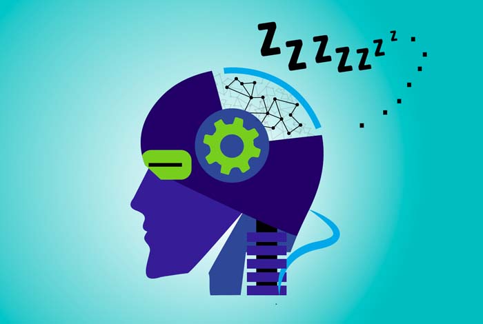
Electric sheep and sleeping androids
I find it impossible to mention that androids might need sleep without reference to Philip K. Dick’s 1968 novel, “Do Androids Dream of Electric Sheep?”; its Wikipedia entry is here.
As it happens, I’m not the only one who felt the need to reference the novel, from a June 8, 2020 news item on ScienceDaily,
No one can say whether androids will dream of electric sheep, but they will almost certainly need periods of rest that offer benefits similar to those that sleep provides to living brains, according to new research from Los Alamos National Laboratory.
“We study spiking neural networks, which are systems that learn much as living brains do,” said Los Alamos National Laboratory computer scientist Yijing Watkins. “We were fascinated by the prospect of training a neuromorphic processor in a manner analogous to how humans and other biological systems learn from their environment during childhood development.”
Watkins and her research team found that the network simulations became unstable after continuous periods of unsupervised learning. When they exposed the networks to states that are analogous to the waves that living brains experience during sleep, stability was restored. “It was as though we were giving the neural networks the equivalent of a good night’s rest,” said Watkins.
…
A June 8, 2020 Los Alamos National Laboratory (LANL) news release (also on EurekAlert), which originated the news item, describes the research team’s presentation,
The discovery came about as the research team worked to develop neural networks that closely approximate how humans and other biological systems learn to see. The group initially struggled with stabilizing simulated neural networks undergoing unsupervised dictionary training, which involves classifying objects without having prior examples to compare them to.
“The issue of how to keep learning systems from becoming unstable really only arises when attempting to utilize biologically realistic, spiking neuromorphic processors or when trying to understand biology itself,” said Los Alamos computer scientist and study coauthor Garrett Kenyon. “The vast majority of machine learning, deep learning, and AI researchers never encounter this issue because in the very artificial systems they study they have the luxury of performing global mathematical operations that have the effect of regulating the overall dynamical gain of the system.”
The researchers characterize the decision to expose the networks to an artificial analog of sleep as nearly a last ditch effort to stabilize them. They experimented with various types of noise, roughly comparable to the static you might encounter between stations while tuning a radio. The best results came when they used waves of so-called Gaussian noise, which includes a wide range of frequencies and amplitudes. They hypothesize that the noise mimics the input received by biological neurons during slow-wave sleep. The results suggest that slow-wave sleep may act, in part, to ensure that cortical neurons maintain their stability and do not hallucinate.
The groups’ next goal is to implement their algorithm on Intel’s Loihi neuromorphic chip. They hope allowing Loihi to sleep from time to time will enable it to stably process information from a silicon retina camera in real time. If the findings confirm the need for sleep in artificial brains, we can probably expect the same to be true of androids and other intelligent machines that may come about in the future.
Watkins will be presenting the research at the Women in Computer Vision Workshop on June 14 [2020] in Seattle.
The 2020 Women in Computer Vition Workshop (WICV) website is here. As is becoming standard practice for these times, the workshop was held in a virtual environment. Here’s a link to and a citation for the poster presentation paper,
Using Sinusoidally-Modulated Noise as a Surrogate for Slow-Wave Sleep to
Accomplish Stable Unsupervised Dictionary Learning in a Spike-Based Sparse Coding Model by Yijing Watkins, Edward Kim, Andrew Sornborger and Garrett T. Kenyon. Women in Computer Vision Workshop on June 14, 2020 in Seattle, Washington (state)
This paper is open access for now.