Tag Archives: solar panels

University of Vermont and the ‘excitons’ of an electron superhighway

This story starts off with one of the current crazes, folding and bendable electronics, before heading off onto the ‘electron highway’. From a Sept. 14, 2015 news item on ScienceDaily (Note: Links have been removed),

TV screens that roll up. Roofing tiles that double as solar panels. Sun-powered cell phone chargers woven into the fabric of backpacks. A new generation of organic semiconductors may allow these kinds of flexible electronics to be manufactured at low cost, says University of Vermont physicist and materials scientist Madalina Furis.

But the basic science of how to get electrons to move quickly and easily in these organic materials remains murky.

To help, Furis and a team of UVM materials scientists have invented a new way to create what they are calling “an electron superhighway” in one of these materials — a low-cost blue dye called phthalocyanine — that promises to allow electrons to flow faster and farther in organic semiconductors.

A Sept. 14, 2015 University of Vermont news release (also on EurekAlert) by Joshua E. Brown, which originated the news item, describes the problem the researches were trying to solve and the solution they found,

Hills and potholes

Many of these types of flexible electronic devices will rely on thin films of organic materials that catch sunlight and convert the light into electric current using excited states in the material called “excitons.” Roughly speaking, an exciton is a displaced electron bound together with the hole it left behind. Increasing the distance these excitons can diffuse — before they reach a juncture where they’re broken apart to produce electrical current — is essential to improving the efficiency of organic semiconductors.

Using a new imaging technique, the UVM team was able to observe nanoscale defects and boundaries in the crystal grains in the thin films of phthalocyanine — roadblocks in the electron highway. “We have discovered that we have hills that electrons have to go over and potholes that they need to avoid,” Furis explains.

To find these defects, the UVM team — with support from the National Science Foundation — built a scanning laser microscope, “as big as a table” Furis says. The instrument combines a specialized form of linearly polarized light and photoluminescence to optically probe the molecular structure of the phthalocyanine crystals.

“Marrying these two techniques together is new; it’s never been reported anywhere,” says Lane Manning ’08 a doctoral student in Furis’ lab and co-author on the new study.

The new technique allows the scientists a deeper understanding of how the arrangement of molecules and the boundaries in the crystals influence the movement of excitons. It’s these boundaries that form a “barrier for exciton diffusion,” the team writes.

And then, with this enhanced view, “this energy barrier can be entirely eliminated,” the team writes. The trick: very carefully controlling how the thin films are deposited. Using a novel “pen-writing” technique with a hollow capillary, the team worked in the lab of UVM physics and materials science professor Randy Headrick to successfully form films with jumbo-sized crystal grains and “small angle boundaries.” Think of these as easy-on ramps onto a highway — instead of an awkward stop sign at the top of a hill — that allow excitons to move far and fast.

Better solar cells

Though the Nature Communications study focused on just one organic material, phthalocyanine, the new research provides a powerful way to explore many other types of organic materials, too — with particular promise for improved solar cells. A recent U.S. Department of Energy report identified one of the fundamental bottlenecks to improved solar power technologies as “determining the mechanisms by which the absorbed energy (exciton) migrates through the system prior to splitting into charges that are converted to electricity.”

The new UVM study — led by two of Furis’ students, Zhenwen Pan G’12, and Naveen Rawat G’15 — opens a window to view how increasing “long-range order” in the organic semiconductor films is a key mechanism that allows excitons to migrate farther. “The molecules are stacked like dishes in a dish rack,” Furis explains, “these stacked molecules — this dish rack — is the electron superhighway.”

Though excitons are neutrally charged — and can’t be pushed by voltage like the electrons flowing in a light bulb — they can, in a sense, bounce from one of these tightly stacked molecules to the next. This allows organic thin films to carry energy along this molecular highway with relative ease, though no net electrical charge is transported.

“One of today’s big challenges is how to make better photovoltaics and solar technologies,” says Furis, who directs UVM’s program in materials science, “and to do that we need a deeper understanding of exciton diffusion. That’s what this research is about.”

Here’s a link to and a citation for the paper,

Polarization-resolved spectroscopy imaging of grain boundaries and optical excitations in crystalline organic thin films by Z. Pan, N. Rawat, I. Cour, L. Manning, R. L. Headrick, & M. Furis. Nature Communications 6, Article number: 8201 doi:10.1038/ncomms9201 Published 14 September 2015

This is an open access article.

Windows as solar panels

Thanks to Dexter Johnson’s Aug. 27, 2015 posting, I’ve found another type of ‘smart’ window (I have written many postings about nanotechnology-enabled windows, especially self-cleaning ones); this window is a solar panel (Note: Links have been removed),

In joint research between the Department of Energy’s Los Alamos National Laboratory (LANL) and the University of Milan-Bicocca (UNIMIB) in Italy, researchers have spent the last 16 months perfecting a technique that makes it possible to embed quantum dots into windows so that the window itself becomes a solar panel.

Of course, this is not the first time someone thought that it would be a good idea to make windows into solar collectors. But this latest iteration marks a significant development in the evolution of the technology. Previous technologies used organic emitters that limited the size of the concentrators to just a few centimeters.

The energy conversion efficiency the researchers were able to acheive with the solar windows was around 3.2 percent, which stands up pretty well when compared with state-of-the-art quantum dot-based solar cells that have reached 9 percent conversion efficiency.

An August 24, 2015 US Los Alamos National Laboratory news release, which inspired Dexter’s posting, describes the research and the US-Italian collaboration in more detail,

A luminescent solar concentrator [LSC] is an emerging sunlight harvesting technology that has the potential to disrupt the way we think about energy; It could turn any window into a daytime power source.

“In these devices, a fraction of light transmitted through the window is absorbed by nanosized particles (semiconductor quantum dots) dispersed in a glass window, re-emitted at the infrared wavelength invisible to the human eye, and wave-guided to a solar cell at the edge of the window,” said Victor Klimov, lead researcher on the project at the Department of Energy’s Los Alamos National Laboratory. “Using this design, a nearly transparent window becomes an electrical generator, one that can power your room’s air conditioner on a hot day or a heater on a cold one.”

… The work was performed by researchers at the Center for Advanced Solar Photophysics (CASP) of Los Alamos, led by Klimov and the research team coordinated by Sergio Brovelli and Francesco Meinardi of the Department of Materials Science of the University of Milan-Bicocca (UNIMIB) in Italy.

The news release goes on to describe the precursor work which made this latest step forward possible,

In April 2014, using special composite quantum dots, the American-Italian collaboration demonstrated the first example of large-area luminescent solar concentrators free from reabsorption losses of the guided light by the nanoparticles. This represented a fundamental advancement with respect to the earlier technology, which was based on organic emitters that allowed for the realization of concentrators of only a few centimeters in size.

However, the quantum dots used in previous proof-of-principle devices were still unsuitable for real-world applications, as they were based on the toxic heavy metal cadmium and were capable of absorbing only a small portion of the solar light. This resulted in limited light-harvesting efficiency and strong yellow/red coloring of the concentrators, which complicated their application in residential environments.

Here’s how they solved the problem (from the news release),

Klimov, CASP’s director, explained how the updated approach solves the coloring problem: “Our new devices use quantum dots of a complex composition which includes copper (Cu), indium (In), selenium (Se) and sulfur (S). This composition is often abbreviated as CISeS. Importantly, these particles do not contain any toxic metals that are typically present in previously demonstrated LSCs.”

“Furthermore,” Klimov noted, “the CISeS quantum dots provide a uniform coverage of the solar spectrum, thus adding only a neutral tint to a window without introducing any distortion to perceived colors. In addition, their near-infrared emission is invisible to a human eye, but at the same time is ideally suited for most common solar cells based on silicon.”

Francesco Meinardi, professor of Physics at UNIMIB, described the emerging work, noting, “In order for this technology to leave the research laboratories and reach its full potential in sustainable architecture, it is necessary to realize non-toxic concentrators capable of harvesting the whole solar spectrum.”

“We must still preserve the key ability to transmit the guided luminescence without reabsorption losses, though, so as to complement high photovoltaic efficiency with dimensions compatible with real windows. The aesthetic factor is also of critical importance for the desirability of an emerging technology,” Meinardi said. [emphasis mine]

I couldn’t agree more with Professor Meinardi. You’re much more likely to adopt something that’s good for you and the planet if you like the look. Following on that thought, you’re much more likely to adopt solar panel windows if they’re aesthetically pleasing.

However, there is still a problem to be solved,

Hunter McDaniel, formerly a Los Alamos CASP postdoctoral fellow and presently a quantum dot entrepreneur (UbiQD founder and president), added, “with a new class of low-cost, low-hazard quantum dots composed of CISeS, we have overcome some of the biggest roadblocks to commercial deployment of this technology.”

“One of the remaining problems to tackle is reducing cost, but already this material is significantly less expensive to manufacture than alternative quantum dots used in previous LSC demonstrations,” McDaniel said.

Nonetheless, they have high hopes the technology can be commercialized (although as Dexter notes, it’s probably not going to be in the near future), from the news release,

A key element of this work is a procedure comparable to the cell casting industrial method used for fabricating high optical quality polymer windows. It involves a new UNIMIB protocol for encapsulating quantum dots into a high-optical quality transparent polymer matrix. The polymer used in this study is a cross-linked polylaurylmethacrylate, which belongs to the family of acrylate polymers. Its long side-chains prevent agglomeration of the quantum dots and provide them with the “friendly” local environment, which is similar to that of the original colloidal suspension. This allows one to preserve light emission properties of the quantum dots upon encapsulation into the polymer.

Sergio Brovelli, the lead researcher on the Italian team, concluded: “Quantum dot solar window technology, of which we had demonstrated the feasibility just one year ago, now becomes a reality that can be transferred to the industry in the short to medium term, allowing us to convert not only rooftops, as we do now, but the whole body of urban buildings, including windows, into solar energy generators.”

“This is especially important in densely populated urban area where the rooftop surfaces are too small for collecting all the energy required for the building operations,” he said. He proposes that the team’s estimations indicate that by replacing the passive glazing of a skyscraper such as the One World Trade Center in NYC (72,000 square meters divided into 12,000 windows) with our technology, it would be possible to generate the equivalent of the energy need of over 350 apartments.

“Add to these remarkable figures, the energy that would be saved by the reduced need for air conditioning thanks to the filtering effect by the LSC, which lowers the heating of indoor spaces by sunlight, and you have a potentially game-changing technology towards “net-zero” energy cities,” Brovelli said.

For anyone interested in this latest work on energy harvesting and windows, here’s a link to and a citation for the paper,

Highly efficient large-area colourless luminescent solar concentrators using heavy-metal-free colloidal quantum dots by Francesco Meinardi, Hunter McDaniel, Francesco Carulli, Annalisa Colombo, Kirill A. Velizhanin, Nikolay S. Makarov, Roberto Simonutti, Victor I. Klimov, & Sergio Brovelli. Nature Nanotechnology (2015) doi:10.1038/nnano.2015.178 Published online 24 August 2015

This paper is behind a paywall.

Solar cells and ‘tinkertoys’

A Nov. 3, 2014 news item on Nanowerk features a project researchers hope will improve photovoltaic efficiency and make solar cells competitive with other sources of energy,

 Researchers at Sandia National Laboratories have received a $1.2 million award from the U.S. Department of Energy’s SunShot Initiative to develop a technique that they believe will significantly improve the efficiencies of photovoltaic materials and help make solar electricity cost-competitive with other sources of energy.

The work builds on Sandia’s recent successes with metal-organic framework (MOF) materials by combining them with dye-sensitized solar cells (DSSC).

“A lot of people are working with DSSCs, but we think our expertise with MOFs gives us a tool that others don’t have,” said Sandia’s Erik Spoerke, a materials scientist with a long history of solar cell exploration at the labs.

A Nov. 3, 2014 Sandia National Laboratories news release, which originated the news item, describes the project and the technology in more detail,

Sandia’s project is funded through SunShot’s Next Generation Photovoltaic Technologies III program, which sponsors projects that apply promising basic materials science that has been proven at the materials properties level to demonstrate photovoltaic conversion improvements to address or exceed SunShot goals.

The SunShot Initiative is a collaborative national effort that aggressively drives innovation with the aim of making solar energy fully cost-competitive with traditional energy sources before the end of the decade. Through SunShot, the Energy Department supports efforts by private companies, universities and national laboratories to drive down the cost of solar electricity to 6 cents per kilowatt-hour.

DSSCs provide basis for future advancements in solar electricity production

Dye-sensitized solar cells, invented in the 1980s, use dyes designed to efficiently absorb light in the solar spectrum. The dye is mated with a semiconductor, typically titanium dioxide, that facilitates conversion of the energy in the optically excited dye into usable electrical current.

DSSCs are considered a significant advancement in photovoltaic technology since they separate the various processes of generating current from a solar cell. Michael Grätzel, a professor at the École Polytechnique Fédérale de Lausanne in Switzerland, was awarded the 2010 Millennium Technology Prize for inventing the first high-efficiency DSSC.

“If you don’t have everything in the DSSC dependent on everything else, it’s a lot easier to optimize your photovoltaic device in the most flexible and effective way,” explained Sandia senior scientist Mark Allendorf. DSSCs, for example, can capture more of the sun’s energy than silicon-based solar cells by using varied or multiple dyes and also can use different molecular systems, Allendorf said.

“It becomes almost modular in terms of the cell’s components, all of which contribute to making electricity out of sunlight more efficiently,” said Spoerke.

MOFs’ structure, versatility and porosity help overcome DSSC limitations

Though a source of optimism for the solar research community, DSSCs possess certain challenges that the Sandia research team thinks can be overcome by combining them with MOFs.

Allendorf said researchers hope to use the ordered structure and versatile chemistry of MOFs to help the dyes in DSSCs absorb more solar light, which he says is a fundamental limit on their efficiency.

“Our hypothesis is that we can put a thin layer of MOF on top of the titanium dioxide, thus enabling us to order the dye in exactly the way we want it,” Allendorf explained. That, he said, should avoid the efficiency-decreasing problem of dye aggregation, since the dye would then be locked into the MOF’s crystalline structure.

MOFs are highly-ordered materials that also offer high levels of porosity, said Allendorf, a MOF expert and 29-year veteran of Sandia. He calls the materials “Tinkertoys for chemists” because of the ease with which new structures can be envisioned and assembled. [emphasis mine]

Allendorf said the unique porosity of MOFs will allow researchers to add a second dye, placed into the pores of the MOF, that will cover additional parts of the solar spectrum that weren’t covered with the initial dye. Finally, he and Spoerke are convinced that MOFs can help improve the overall electron charge and flow of the solar cell, which currently faces instability issues.

“Essentially, we believe MOFs can help to more effectively organize the electronic and nano-structure of the molecules in the solar cell,” said Spoerke. “This can go a long way toward improving the efficiency and stability of these assembled devices.”

In addition to the Sandia team, the project includes researchers at the University of Colorado-Boulder, particularly Steve George, an expert in a thin film technology known as atomic layer deposition.

The technique, said Spoerke, is important in that it offers a pathway for highly controlled materials chemistry with potentially low-cost manufacturing of the DSSC/MOF process.

“With the combination of MOFs, dye-sensitized solar cells and atomic layer deposition, we think we can figure out how to control all of the key cell interfaces and material elements in a way that’s never been done before,” said Spoerke. “That’s what makes this project exciting.”

Here’s a picture showing an early Tinkertoy set,

Original Tinkertoy, Giant Engineer #155. Questor Education Products Co., c.1950 [downloaded from http://en.wikipedia.org/wiki/Tinkertoy#mediaviewer/File:Tinkertoy_300126232168.JPG]

Original Tinkertoy, Giant Engineer #155. Questor Education Products Co., c.1950 [downloaded from http://en.wikipedia.org/wiki/Tinkertoy#mediaviewer/File:Tinkertoy_300126232168.JPG]

The Tinkertoy entry on Wikipedia has this,

The Tinkertoy Construction Set is a toy construction set for children. It was created in 1914—six years after the Frank Hornby’s Meccano sets—by Charles H. Pajeau and Robert Pettit and Gordon Tinker in Evanston, Illinois. Pajeau, a stonemason, designed the toy after seeing children play with sticks and empty spools of thread. He and Pettit set out to market a toy that would allow and inspire children to use their imaginations. At first, this did not go well, but after a year or two over a million were sold.

Shrinky Dinks, tinkertoys, Lego have all been mentioned here in conjunction with lab work. I’m always delighted to see scientists working with or using children’s toys as inspiration of one type or another.

Fishnet of gold atoms improves solar cell performance

Apparently they’re calling the University of Western Ontario by a new name, Western University. Given the university’s location in what is generally acknowledged as central Canada or, sometimes, as eastern Canada, this seems like a geographically confusing approach not only in Canada but elsewhere too. After all, more than one country boasts a ‘west’.

A Sept. 26, 2014 news item on Nanowerk highlights new work on improving solar cell performance (Note: A link has been removed),

Scientists at Western University [Ontario, Canada] have discovered that a small molecule created with just 144 atoms of gold can increase solar cell performance by more than 10 per cent. These findings, published recently by the high-impact journal Nanoscale (“Tessellated gold nanostructures from Au144(SCH2CH2Ph)60 molecular precursors and their use in organic solar cell enhancement”), represent a game-changing innovation that holds the potential to take solar power mainstream and dramatically decrease the world’s dependence on traditional, resource-based sources of energy, says Giovanni Fanchini from Western’s Faculty of Science.

For those of us who remember ‘times tables’, the number 144 can have a special meaning as it is the last number (’12’ times ’12’ equals ‘144’) one was obliged to memorize. At least, that was true at my school in Vancouver, Canada but perhaps not elsewhere, eh?

Getting back to the ‘fishnet’, a Sept. 25, 2014 Western University news release, which originated the news item, expands the business possibilities for this work,

Fanchini, the Canada Research Chair in Carbon-based Nanomaterials and Nano-optoelectronics, says the new technology could easily be fast-tracked and integrated into prototypes of solar panels in one to two years and solar-powered phones in as little as five years.

“Every time you recharge your cell phone, you have to plug it in,” says Fanchini, an assistant professor in Western’s Department of Physics and Astronomy. “What if you could charge mobile devices like phones, tablets or laptops on the go? Not only would it be convenient, but the potential energy savings would be significant.”

The Western researchers have already started working with manufacturers of solar components to integrate their findings into existing solar cell technology and are excited about the potential.

“The Canadian business industry already has tremendous know-how in solar manufacturing,” says Fanchini. “Our invention is modular, an add-on to the existing production process, so we anticipate a working prototype very quickly.”

The news release then gives a few technical details,

Making nanoplasmonic enhancements, Fanchini and his team use “gold nanoclusters” as building blocks to create a flexible network of antennae on more traditional solar panels to attract an increase of light. While nanotechnology is the science of creating functional systems at the molecular level, nanoplasmonics investigates the interaction of light with and within these systems.

“Picture an extremely delicate fishnet of gold,” explains Fanchini explains, noting that the antennae are so miniscule they are unseen even with a conventional optical microscope. “The fishnet catches the light emitted by the sun and draws it into the active region of the solar cell.”

According to Fanchini, the spectrum of light reflected by gold is centered on the yellow colour and matches the light spectrum of the sun making it superior for such antennae as it greatly amplifies the amount of sunlight going directly into the device.

“Gold is very robust, resilient to oxidization and not easily damaged, making it the perfect material for long-term use,” says Fanchini. “And gold can also be recycled.”

It has been known for some time that larger gold nanoparticles enhance solar cell performance, but the Western team is getting results with “a ridiculously small amount” – approximately 10,000 times less than previous studies, which is 10,000 times less expensive too.

I hope to hear about a working prototype soon. Meanwhile, here’s a link to and a citation for the paper,

Tessellated gold nanostructures from Au144(SCH2CH2Ph)60 molecular precursors and their use in organic solar cell enhancement by Reg Bauld, Mahdi Hesari, Mark S. Workentin, and Giovanni Fanchini. Nanoscale, 2014,6, 7570-7575 DOI: 10.1039/C4NR01821D
First published online 06 May 2014

This paper is behind a paywall.

One final comment, it seems like a long lead time between publication of the paper and publicity. I wonder if the paper failed to get notice in May 2014, assuming there was a campaign at the time, or if this is considered a more optimal time period for getting noticed.

Wearable solar panels with perovskite

There was a bit of a flutter online in late July 2014 about solar cell research and perovskite, a material that could replace silicon therefore making solar cells more affordable, which hopefully would lead to greater adoption of the technology. Happily, the publishers of the study seem to have reissued their news release (h/t Aug. 11, 2014 news item on Nanwerk).

From the Wiley online press release Nr. 29/2014,

Textile solar cells are an ideal power source for small electronic devices incorporated into clothing. In the journal Angewandte Chemie, Chinese scientists have now introduced novel solar cells in the form of fibers that can be woven into a textile. The flexible, coaxial cells are based on a perovskite material and carbon nanotubes; they stand out due to their excellent energy conversion efficiency of 3.3 % and their low production cost.

The dilemma for solar cells: they are either inexpensive and inefficient, or they have a reasonable efficiency and are very expensive. One solution may come from solar cells made of perovskite materials, which are less expensive than silicon and do not require any expensive additives. Perovskites are materials with a special crystal structure that is like that of perovskite, a calcium titanate. These structures are often semiconductors and absorb light relatively efficiently. Most importantly, they can move electrons excited by light for long distances within the crystal lattice before they return to their energetic ground state and take up a solid position – a property that is very important in solar cells.

A team led by Hisheng Peng at Fudan University in Shanghai has now developed perovskite solar cells in the form of flexible fibers that can be woven into electronic textiles. Their production process is relatively simple and inexpensive because it uses a solution-based process to build up the layers.

The anode is a fine stainless steel wire coated with a compact n-semiconducting titanium dioxide layer. A layer of porous nanocrystalline titanium dioxide is deposited on top of this. This provides a large surface area for the subsequent deposition of the perovskite material CH3NH3PbI3. This is followed by a layer made of a special organic material. Finally a transparent layer of aligned carbon nanotubes is continuously wound over the whole thing to act as the cathode. The resulting fiber is so fine and flexible that it can be woven into textiles.

The perovskite layer absorbs light, that excites electrons and sets them free, causing a charge separation between the electrons and the formally positively charged “holes” The electrons enter the conducting band of the compact titanium dioxide layer and move to the anode. The “holes” are captured by the organic layer. The large surface area and the high electrical conductivity of the carbon nanotube cathode aid in the rapid conduction of the charges with high photoelectric currents. The fiber solar cell can attain an energy conversion efficiency of 3.3 %, exceeding that of all previous coaxial fiber solar cells made with either dyes or polymers.

Here’s an image used in the press release illustrating the new fiber,

[downloaded from http://www.wiley-vch.de/vch/journals/2002/press/201429press.pdf]

[downloaded from http://www.wiley-vch.de/vch/journals/2002/press/201429press.pdf]

Here’s a link to and a citation for the paper,

Integrating Perovskite Solar Cells into a Flexible Fiber by Longbin Qiu, Jue Deng, Xin Lu, Zhibin Yang, and Prof. Huisheng Peng. Angewandte Chemie International Edition DOI: 10.1002/anie.201404973 Article first published online: 22 JUL 2014

© 2014 WILEY-VCH Verlag GmbH & Co. KGaA, Weinheim

This paper is behind a paywall.

I found a second item about perovskite and solar cells in a May 16, 2014 article by Vicki Marshall for Chemistry World which discussed some research in the UK (Note: Links have been removed),

A lead-free and non-toxic alternative to current perovskite solar-cell technology has been reported by researchers in the UK: tin halide perovskite solar cells. They are also cheaper to manufacture than the silicon solar cells currently dominating the market.

Nakita Noel, part of Henry Snaith’s research team at the University of Oxford, describes how perovskite materials have caused a bit of a whirlwind since they came out in 2009: ‘Everybody that’s working in the solar community is looking to beat silicon.’ Despite the high efficiency of conventional crystalline silicon solar cells (around 20%), high production and installation costs decrease their economic feasibility and widespread use.

The challenge to find a cheaper alternative led to the development of perovskite-based solar cells, as organic–inorganic metal trihalide perovskites have both abundant and cheap starting materials. However, the presence of lead in some semiconductors could create toxicology issues in the future. As Noel puts it ‘every conference you present at somebody is bound to put up their hand and ask “What about the lead – isn’t this toxic?”’

Brian Hardin, co-founder of PLANT PV, US, and an expert in new materials for photovoltaic cells, says the study ‘should be considered a seminal work on alternative perovskites and is extremely valuable to the field as they look to better understand how changes in chemistry affect solar cell performance and stability.’

Here’s a link to and a citation for the UK researchers’ paper,

Lead-free organic–inorganic tin halide perovskites for photovoltaic applications by Nakita K. Noel, Samuel D. Stranks, Antonio Abate, Christian Wehrenfennig, Simone Guarnera, Amir-Abbas Haghighirad, Aditya Sadhana, Giles E. Eperon, Sandeep K. Pathak, Michael B. Johnston, Annamaria Petrozza, Laura M. Herza, and Henry J. Snaith. Energy Environ. Sci., 2014, Advance Article DOI: 10.1039/C4EE01076K First published online 01 May 2014

This article was open access until June 27, 2014 but now it is behind a paywall.

I notice there’s no mention of lead in the materials describing the research paper from the Chinese scientists. Perhaps they were working with lead-free materials.

Solar cells and copper sprouts

First, Washington University in St. Louis (WUSTL; located in Missouri, US) announced a discovery about solar cells, then, the university announced a commitment to increase solar output by Fall 2014. Whether these two announcements are linked by some larger policy or strategy is not clear to me but it’s certainly an interesting confluence of events.

An April 26, 2014 news item on Azonano describes the researchers’ discovery,

By looking at a piece of material in cross section, Washington University in St. Louis engineer Parag Banerjee, PhD, and his team discovered how copper sprouts grass-like nanowires that could one day be made into solar cells.

Banerjee, assistant professor of materials science and an expert in working with nanomaterials, Fei Wu, graduate research assistant, and Yoon Myung, PhD, a postdoctoral research associate, also took a step toward making solar cells and more cost-effective.

An April 21, 2014 WUSTL news release by Beth Miller, which originated the news item, describes the research in some detail,

Banerjee and his team worked with copper foil, a simple material similar to household aluminum foil. When most metals are heated, they form a thick metal oxide film. However, a few metals, such as copper, iron and zinc, grow grass-like structures known as nanowires, which are long, cylindrical structures a few hundred nanometers wide by many microns tall. They set out to determine how the nanowires grow.

“Other researchers look at these wires from the top down,” Banerjee says. “We wanted to do something different, so we broke our sample and looked at it from the side view to see if we got different information, and we did.”

The team used Raman spectroscopy, a technique that uses light from a laser beam to interact with molecular vibrations or other movements. They found an underlying thick film made up of two different copper oxides (CuO and Cu2O) that had narrow, vertical columns of grains running through them. In between these columns, they found grain boundaries that acted as arteries through which the copper from the underlying layer was being pushed through when heat was applied, creating the nanowires.

“We’re now playing with this ionic transport mechanism, turning it on and off and seeing if we can get some different forms of wires,” says Banerjee, who runs the Laboratory for Emerging and Applied Nanomaterials (L.E.A.N.).

Like solar cells, the nanowires are single crystal in structure, or a continuous piece of material with no grain boundaries, Banerjee says.

“If we could take these and study some of the basic optical and electronic properties, we could potentially make solar cells,” he says. “In terms of optical properties, copper oxides are well-positioned to become a solar energy harvesting material.”

This work may be useful in other applications according to the news release,

The find may also benefit other engineers who want to use single crystal oxides in scientific research. Manufacturing single crystal Cu2O for research is very expensive, Banerjee says, costing up to about $1,500 for one crystal.

“But if you can live with this form that’s a long wire instead of a small crystal, you can really use it to study basic scientific phenomena,” Banerjee says.

Banerjee’s team also is looking for other uses for the nanowires, including acting as a semiconductor between two materials, as a photocatalyst, a photovoltaic or an electrode for splitting water.

Here’s a link to and a citation for the paper,

Unravelling transient phases during thermal oxidation of copper for dense CuO nanowire growth by Fei Wu, Yoon Myunga and Parag Banerjee.  CrystEngComm, 2014,16, 3264-3267. DOI: 10.1039/C4CE00275J First published online 26 Feb 2014

This article is behind a paywall.

Shortly after the research announcement, WUSTL made this ‘solar’ announcement via an April 29, 2014 news release by Neil Schoenherr,

Washington University in St. Louis is moving forward with a bold and impactful plan to increase solar output on all campuses by 1,150 percent over current levels by this fall. The project demonstrates the university’s commitment to sustainable operations and to reducing its environmental impact in the St. Louis region and beyond.

This spring and early summer, the university will add a total of 379 kilowatts (kw) of solar on university-owned property throughout the region. Prior to this installation, the university had 33 kw that were installed as demonstration projects.

I suspect the two announcements reflect synchronicity or, perhaps, my tendency to see and develop patterns.

Infusing solar cells with beauty

There is a bit of a theme emerging (if two news items some six months apart can be considered a theme) with scientists now trying to make solar cells or solar panels (as per my July 3, 2013 posting) objects of beauty. The latest project is from the University of Michigan according to a March 4, 2014 news item on ScienceDaily,

Colorful, see-through solar cells invented at the University of Michigan could one day be used to make stained-glass windows, decorations and even shades that turn the sun’s energy into electricity.

The cells, believed to be the first semi-transparent, colored photovoltaics, have the potential to vastly broaden the use of the energy source, says Jay Guo, a professor of electrical engineering and computer science, mechanical engineering, and macromolecular science and engineering at U-M. Guo is lead author of a paper about the work newly published online in Scientific Reports.

Here’s a video (from the University of Michigan) where Jay Guo describes his work,

For those who are too impatient to watch the video, here’s some of what was discussed along with  additional technical detail from a March 3, 2014 University of Michigan news release, which originated the news item,

“I think this offers a very different way of utilizing solar technology rather than concentrating it in a small area,” he said. “Today, solar panels are black and the only place you can put them on a building is the rooftop. And the rooftop of a typical high-rise is so tiny.

“We think we can make solar panels more beautiful—any color a designer wants. And we can vastly deploy these panels, even indoors.”

Guo envisions them on the sides of buildings, as energy-harvesting billboards and as window shades—a thin layer on homes and cities. Such an approach, he says, could be especially attractive in densely populated cities.

In a palm-sized American flag slide, the team demonstrated the technology.

“All the red stripes, the blue background and so on—they are all working solar cells,” Guo said.

The Stars and Stripes achieved 2 percent efficiency. A meter-square panel could generate enough electricity to power fluorescent light bulbs and small electronic gadgets, Guo says. State-of-the art organic cells in research labs are roughly 10 percent efficient.

The researchers are working to improve their numbers with new materials, but there will always be a tradeoff between beauty and utility in this case. Traditional black solar cells absorb all wavelengths of visible light. Guo’s cells are designed to transmit, or—in other versions—reflect certain colors, so by nature they’re kicking energy from those wavelengths back out to our eyes rather than converting it to electricity.

Unlike other color solar cells, Guo’s don’t rely on dyes or microstructures that can blur the image behind them. The cells are mechanically structured to transmit certain light wavelengths. To get different colors, they varied the thickness of the semiconductor layer of amorphous silicon in the cells. The blue regions are six nanometers thick while the red is 31 (the team also made green, but that color isn’t in the flag).

Amorphous silicon is commonly used in screens on cell phones, laptops and large LCD screens, in addition to solar cells. They sandwiched an ultrathin sheet of it between two semi-transparent electrodes that could let light in and also carry away the electrical current.

One of these so-called charge transport layers is made of an organic material. This hybrid structure, a combination of both organic and inorganic components, lets the researchers make cells that are 10 times thinner than traditional amorphous silicon solar cells. The organic layer replaces a thick ‘doped’ region that would typically controls the flow of electricity.

The ultrathin, hybrid design helps the cells hold their color and leads to a nearly 100 percent quantum efficiency. Quantum efficiency is different from overall efficiency. It refers to the percentage of light particles the device catches that lead to electrical current in that charge transport layer. Solar cells can leak current after this point, but researchers strive for a high number.

The cells’ hues don’t change based on viewing angle, which is important for several reasons. It means manufacturers could lock in color for precise pictures or patterns. It’s also a sign that the devices are soaking up the same amount of light regardless of where the sun is in the sky. Conventional solar panels pivot across the day to track rays.

“Solar energy is essentially inexhaustible, and it’s the only energy source that can sustain us long-term,” Guo said. “We have to figure out how to use as much of it as we can.”

Here’s a link to and a citation for the paper,

Decorative power generating panels creating angle insensitive transmissive colors by Jae Yong Lee, Kyu-Tae Lee, Sungyong Seo, & L. Jay Guo. Scientific Reports 4, Article number: 4192 doi:10.1038/srep04192 Published 28 February 2014

This paper is open access.

Making solar panels beautiful

Researchers at Germany’s Fraunhofer Institute for Applied Optics and Precision Engineering IOF in Jena are working on ways to make solar panels more aesthetically pleasing according to a July 1, 2013 news item on Azonano,

Until now, designers of buildings have no choice but to use black or bluish-gray colored solar panels. With the help of thin-film technologies, researchers have now been able to turn solar cells into colorful creations.

Covering a roof or a façade with standard solar cells to generate electricity will change a building’s original appearance – and not always for the better. At present only dark solar panels are widely available on the market. “Not enough work has been done so far on combining photovoltaics and design elements to really do the term ‘customized photovoltaics’ justice,” says Kevin Füchsel, project manager at the Fraunhofer Institute for Applied Optics and Precision Engineering IOF in Jena.

But things are changing. The IOF physicist has been focusing for the last four years on nanostructured solar cells suitable for mass production as part of a junior research group funded by Germany’s Federal Ministry for Education and Research (BMBF). Together with a Fraunhofer team and scientists from the Friedrich-Schiller University in Jena, the group of optics specialists is looking for cost-effective techniques and manufacturing processes to increase both the efficiency of solar panels and the design flexibility they give architects and designers.

Here’s photomontage illustrating Füchsel’s ideas,

The photomontage shows how the Fraunhofer IAO building in Stuttgart could be fitted with an “efficient design” solar façade. © Fraunhofer IOF

The photomontage shows how the Fraunhofer IAO building in Stuttgart could be fitted with an “efficient design” solar façade.
© Fraunhofer IOF

The July 1, 2013 Fraunhofer Institute news release, which originated the news item, describes Füchsel’s work in more detail,

Füchsel is currently working with his “efficient design” team on the fundamentals of how to make colored solar cells from paper-thin silicon wafers. These will be particularly suited to designs for decorative façades and domestic roofs. The silicon semiconductor material, just a few micrometers thick, absorbs light and turns it into electricity. To enable lots of light to reach the silicon substrate, the semiconductor layer is given an optically neutral protective barrier (insulator), onto which a hundred-nanometer-thick oxide layer is applied. This transparent conductive oxide (TCO) conducts electricity, and is there primarily to guide as many light particles as possible to the semiconductor layer below. “TCO has a lower refractive index than silicon, so it works as an anti-reflective coating,” Füchsel says.

The simple construction of this SIS (semiconductor-insulator-semiconductor) solar cell, with its transparent outer layer, has a further advantage: Not only does it capture more light, it means solar panels can be made in different colors and shapes. “The color comes from changing the physical thickness of the transparent conductive oxide layer, or modifying its refractive index,” Füchsel says. The Jena-based researchers have thus managed to combine wafer-based silicon with processes borrowed from thin-film photovoltaics. They are also pioneering the use of innovative coating materials. Indium tin oxide is the most common material used today, but it is expensive.  The IOF laboratory is working on how to use cheaper zinc oxide with added aluminum. New opportunities in façade design are being opened up not just by SIS solar cells, however, but also by dye solar modules and flexible organic solar cells.

But how does color affect the efficiency of these new SIS modules? “Giving solar cells color doesn’t really affect their efficiency. The additional transparent TCO layer has barely any impact on the current yield,” Füchsel says. Simulations showed that SIS cells could be up to 20 percent efficient. In practice, the efficiency depends on the design of the solar panels and the direction the building faces. But not every color allows you to generate the same amount of electricity. There are restrictions for example with certain blends of red, blue and green.

To connect several solar cells to create a single module the IOF scientist will use laser-based optical welding processes. They enable accurate work at a micrometer scale and do not damage the surrounding material. Researchers are also developing an inkjet printing process to contact the conductive TCO later on the silicon wafer. This will make manufacturing faster and allow additional degrees of flexibility in design. SIS solar cells could even be used to make large billboards that produce their own electricity. Patents already cover the production of colored cells, as well as the ability to integrate design elements into solar panels and whole modules. “This opens up numerous possibilities to use a building to communicate information, displaying the name of a company or even artistic pictures,” Füchsel says.

I look forward to a more beautiful future.

Spinach + Silicon = Green Power

I wouldn’t expect that anyone will be turning their spinach salads into hybrid solar cells anytime soon despite what scientists at Vanderbilt University (Tennessee) have achieved. From the Sept. 4, 2012 news release on EurekAlert,

An interdisciplinary team of researchers at Vanderbilt University have developed a way to combine the photosynthetic protein that converts light into electrochemical energy in spinach with silicon, the material used in solar cells, in a fashion that produces substantially more electrical current than has been reported by previous “biohybrid” solar cells.

Here’s an illustration of the concept provided by Vanderbilt University,

(Julie Turner/Vanderbilt)

According to the Sept. 4, 2012 Vanderbilt University news release , the researchers were trying exploit a feature of a protein found in spinach (and other plants),

More than 40 years ago, scientists discovered that one of the proteins involved in photosynthesis, called Photosystem 1 (PS1), continued to function when it was extracted from plants like spinach. Then they determined PS1 converts sunlight into electrical energy with nearly 100 percent efficiency, compared to conversion efficiencies of less than 40 percent achieved by manmade devices. This prompted various research groups around the world to begin trying to use PS1 to create more efficient solar cells.

When a PS1 protein exposed to light, it absorbs the energy in the photons and uses it to free electrons and transport them to one side of the protein. That creates regions of positive charge, called holes, which move to the opposite side of the protein.

In a leaf, all the PS1 proteins are aligned. But in the protein layer on the device, individual proteins are oriented randomly. Previous modeling work indicated that this was a major problem. When the proteins are deposited on a metallic substrate, those that are oriented in one direction provide electrons that the metal collects while those that are oriented in the opposite direction pull electrons out of the metal in order to fill the holes that they produce. As a result, they produce both positive and negative currents that cancel each other out to leave a very small net current flow.

The problem with using a metallic substrate was addressed by using and ‘doping’ silicon (from the Vanderbilt University news release),

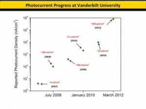
The Vanderbilt researchers report that their PS1/silicon combination produces nearly a milliamp (850 microamps) of current per square centimeter at 0.3 volts. That is nearly two and a half times more current than the best level reported previously from a biohybrid cell. The reason this combo works so well is because the electrical properties of the silicon substrate have been tailored to fit those of the PS1 molecule. This is done by implanting electrically charge atoms in the silicon to alter its electrical properties: a process called “doping.” In this case, the protein worked extremely well with silicon doped with positive charges and worked poorly with negatively doped silicon.

To make the device, the researchers extracted PS1 from spinach into an aqueous solution and poured the mixture on the surface of a p-doped silicon wafer. Then they put the wafer in a vacuum chamber in order to evaporate the water away leaving a film of protein. They found that the optimum thickness was about one micron, about 100 PS1 molecules thick.

Here’s a graph illustrating the improvement (larger version available here),

Graph shows the dramatic increase in electrical current that Vanderbilt researchers have managed to produce from biohybrid solar cells. (Courtesy of Cliffel Lab/Vanderbilt University)

Encouraging news overall but the researchers still have more work to do (from the Vanderbilt University news release),

This combination produces current levels almost 1,000 times higher than we were able to achieve by depositing the protein on various types of metals. It also produces a modest increase in voltage,” said David Cliffel, associate professor of chemistry, who collaborated on the project with Kane Jennings, professor of chemical and biomolecular engineering.

“If we can continue on our current trajectory of increasing voltage and current levels, we could reach the range of mature solar conversion technologies in three years.”

The researchers’ next step is to build a functioning PS1-silicon solar cell using this new design. Jennings has an Environmental Protection Agency award that will allow a group of undergraduate engineering students to build the prototype. The students won the award at the National Sustainable Design Expo in April based on a solar panel that they had created using a two-year old design. With the new design, Jennings estimates that a two-foot panel could put out at least 100 milliamps at one volt – enough to power a number of different types of small electrical devices.

So, our solar cells are going to become more and more plantlike? I can certainly see the appeal if it means minimizing dependency on “rare and expensive materials like platinum or indium” as per the Vanderbilt University news release.

Using your microwave for DIY (do it yourself) solar panels?

The researchers at Oregon State University seem to think that their discovery will scale up to commercial levels for manufacturing solar panels that are cheaper and easier. Still, if all you need is a microwave, then I imagine some enterprising do-it-yourselfer will give this technique a try.

Microwave oven

This microwave oven technology is being used to produce solar cells with less energy, expense and environmental concerns. (Photo courtesy of Oregon State University Copied from: http://www.flickr.com/photos/oregonstateuniversity/7841150094/in/photostream)

From the Aug. 24, 2012 news item on Nanowerk,

The same type of microwave oven technology that most people use to heat up leftover food has found an important application in the solar energy industry, providing a new way to make thin-film photovoltaic products with less energy, expense and environmental concerns.

Engineers at Oregon State University have for the first time developed a way to use microwave heating in the synthesis of copper zinc tin sulfide, a promising solar cell compound that is less costly and toxic than some solar energy alternatives.

The Oregon State University Aug. 24, 2012 news release which originated the news item provides additional detail about the technology and future plans for commercializing it,

“All of the elements used in this new compound are benign and inexpensive, and should have good solar cell performance,” said Greg Herman, an associate professor in the School of Chemical, Biological and Environmental Engineering at OSU.

“Several companies are already moving in this direction as prices continue to rise for some alternative compounds that contain more expensive elements like indium,” he said. “With some improvements in its solar efficiency this new compound should become very commercially attractive.”

These thin-film photovoltaic technologies offer a low cost, high volume approach to manufacturing solar cells. A new approach is to create them as an ink composed of nanoparticles, which could be rolled or sprayed – by approaches such as old-fashioned inkjet printing – to create solar cells. [emphasis mine]

To further streamline that process, researchers have now succeeded in using microwave heating, instead of conventional heating, to reduce reaction times to minutes or seconds, and allow for great control over the production process. This “one-pot” synthesis is fast, cheap and uses less energy, researchers say, and has been utilized to successfully create nanoparticle inks that were used to fabricate a photovoltaic device.

From a do-it-yourself point of view, this technology sounds even more promising with the mention of an inkjet printer.