Tag Archives: SWCNTs

Colo(u)ring your carbon nanotubes

Finnish research is highlighted in an August 28, 2018 news item on phys.org,

A method developed at Aalto University, Finland, can produce large quantities of pristine single-walled carbon nanotubes in select shades of the rainbow. The secret is a fine-tuned fabrication process—and a small dose of carbon dioxide. The films could find applications in touch screen technologies or as coating agents for new types of solar cells.

An August 28, 2018 Aalto University press release (also on EurekAlert), which originated the news item, provides more detail,

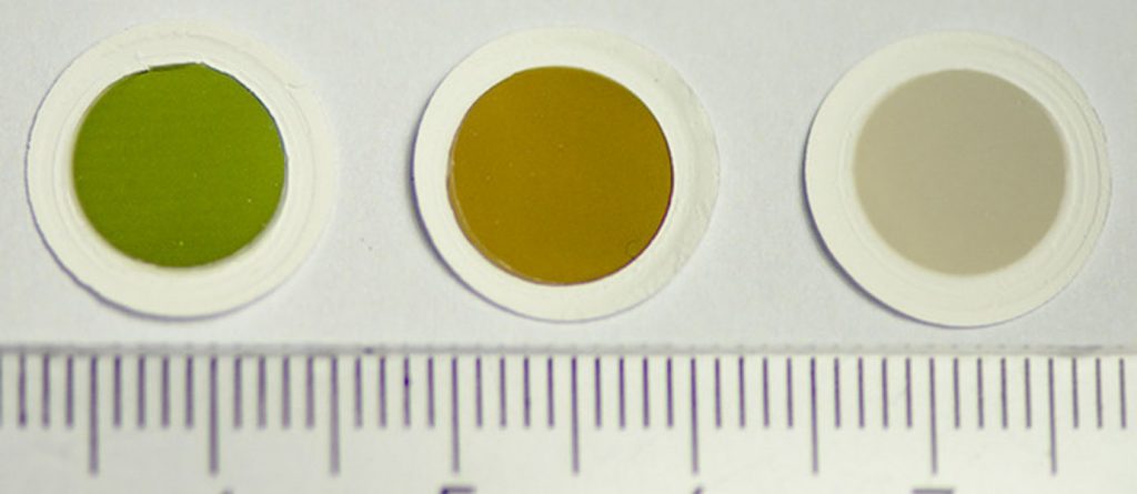
Samples of the colourful carbon nanotube thin films, as produced in the fabrication reactor. Image: Aalto University.
 

Single-walled carbon nanotubes, or sheets of one atom-thick layers of graphene rolled up into different sizes and shapes, have found many uses in electronics and new touch screen devices. By nature, carbon nanotubes are typically black or a dark grey.

In their new study published in the Journal of the American Chemical Society (JACS), Aalto University researchers present a way to control the fabrication of carbon nanotube thin films so that they display a variety of different colours—for instance, green, brown, or a silvery grey.

The researchers believe this is the first time that coloured carbon nanotubes have been produced by direct synthesis. Using their invention, the colour is induced straight away in the fabrication process, not by employing a range of purifying techniques on finished, synthesized tubes.

With direct synthesis, large quantities of clean sample materials can be produced while also avoiding damage to the product in the purifying process—which makes it the most attractive approach for applications.

‘In theory, these coloured thin films could be used to make touch screens with many different colours, or solar cells that display completely new types of optical properties,’ says Esko Kauppinen, Professor at Aalto University.

To get carbon structures to display colours is a feat in itself. The underlying techniques needed to enable the colouration also imply finely detailed control of the structure of the nanotube structures. Kauppinen and his team’s unique method, which uses aerosols of metal and carbon, allows them to carefully manipulate and control the nanotube structure directly from the fabrication process.

‘Growing carbon nanotubes is, in a way, like planting trees: we need seeds, feeds, and solar heat. For us, aerosol nanoparticles of iron work as a catalyst or seed, carbon monoxide as the source for carbon, so feed, and a reactor gives heat at a temperature more than 850 degrees Celsius,’ says Dr. Hua Jiang, Senior Scientist at Aalto University.

Professor Kauppinen’s group has a long history of using these very resources in their singular production method. To add to their repertoire, they have recently experimented with administering small doses of carbon dioxide into the fabrication process.

‘Carbon dioxide acts as a kind of graft material that we can use to tune the growth of carbon nanotubes of various colors,’ explains Jiang.

With an advanced electron diffraction technique, the researchers were able to find out the precise atomic scale structure of their thin films. They found that they have very narrow chirality distributions, meaning that the orientation of the honeycomb-lattice of the tubes’ walls is almost uniform throughout the sample. The chirality more or less dictates the electrical properties carbon nanotubes can have, as well as their colour.

The method developed at Aalto University promises a simple and highly scalable way to fabricate carbon nanotube thin films in high yields.

‘Usually you have to choose between mass production or having good control over the structure of carbon nanotubes. With our breakthrough, we can do both,’ trusts Dr. Qiang Zhang, a postdoctoral researcher in the group.

Follow-up work is already underway.

‘We want to understand the science of how the addition of carbon dioxide tunes the structure of the nanotubes and creates colours. Our aim is to achieve full control of the growing process so that single-walled carbon nanotubes could be used as building blocks for the next generation of nanoelectronics devices,’ says professor Kauppinen.

Here’s a link to and a citation for the paper,

Direct Synthesis of Colorful Single-Walled Carbon Nanotube Thin Films by Yongping Liao, Hua Jiang, Nan Wei, Patrik Laiho, Qiang Zhang, Sabbir A. Khan, and Esko I. Kauppinen. J. Am. Chem. Soc., 2018, 140 (31), pp 9797–9800 DOI: 10.1021/jacs.8b05151 Publication Date (Web): July 26, 2018

Copyright © 2018 American Chemical Society

This paper appears to be open access.

For the curious, here’s a peek at the coloured carbon nanotube films,


Caption: Samples of the colorful carbon nanotube thin films, as produced in the fabrication reactor. Credit: Authors / Aalto University

Carbon nanotubes: faster, cheaper, easier, and more consistent

One of the big problems with nanomaterials has to do with production issues such as: consistent size and shape. It seems that scientists at the US National Institute of Standards and Technology (NIST) have developed a technique for producing carbon nanotubes (CNTs) which addresses these issues. From a July 19, 2016 news item on Nanotechnology Now,

Just as many of us might be resigned to clogged salt shakers or rush-hour traffic, those working to exploit the special properties of carbon nanotubes have typically shrugged their shoulders when these tiniest of cylinders fill with water during processing. But for nanotube practitioners who have reached their Popeye threshold and “can’t stands no more,” the National Institute of Standards and Technology (NIST) has devised a cheap, quick and effective strategy that reliably enhances the quality and consistency of the materials–important for using them effectively in applications such as new computing technologies.

To prevent filling of the cores of single-wall carbon nanotubes with water or other detrimental substances, the NIST researchers advise intentionally prefilling them with a desired chemical of known properties. Taking this step before separating and dispersing the materials, usually done in water, yields a consistently uniform collection of nanotubes. In quantity and quality, the results are superior to water-filled nanotubes, especially for optical applications such as sensors and photodetectors.

A July 15, 2016 NIST news release, which originated the news item, expands on the theme,

The approach opens a straightforward route for engineering the properties of single-wall carbon nanotubes—rolled up sheets of carbon atoms arranged like chicken wire or honey combs—with improved or new properties.

“This approach is so easy, inexpensive and broadly useful that I can’t think of a reason not to use it,” said NIST chemical engineer Jeffrey Fagan.

In their proof-of-concept experiments, the NIST team inserted more than 20 different compounds into an assortment of single-wall carbon nanotubes with an interior diameter that ranged from more than 2 down to about 0.5 nanometers. Led by visiting researcher Jochen Campo, the scientists tested their strategy by using hydrocarbons called alkanes as fillers.

The alkanes, which include such familiar compounds as propane and butane, served to render the nanotube interiors unreactive. In other words, the alkane-filled nanotubes behaved almost as if they were empty—precisely the goal of Campo, Fagan and colleagues.

Compared with nanotubes filled with water and possibly ions, acids and other unwanted chemicals encountered during processing, empty nanotubes possess far superior properties. For example, when stimulated by light, empty carbon nanotubes fluoresce far brighter and with sharper signals.

Yet, “spontaneous ingestion” of water or other solvents by the nanotubes during processing is an “endemic but often neglected phenomenon with strong implications for the development of nanotube applications,” the NIST team wrote in a recent article in Nanoscale Horizons.

Perhaps because of the additional cost and effort required to filter out and gather nanotubes, researchers tend to tolerate mixed batches of unfilled (empty) and mostly filled single-wall carbon nanotubes. Separating unfilled nanotubes from these mixtures requires expensive ultracentrifuge equipment and, even then, the yield is only about 10 percent, Campo estimates.

“If your goal is to use nanotubes for electronic circuits, for example, or for fluorescent anti-cancer image contrast agents, then you require much greater quantities of materials of consistent composition and quality,” Campo explained, who was exploring these applications while doing postdoctoral research at the University of Antwerp. “This particular need inspired development of the new prefilling method by asking the question, can we put some passive chemical into the nanotube instead to keep the water out.”

From the very first simple experiments, the answer was yes. And the benefits can be significant. In fluorescence experiments, alkane-filled nanotubes emitted signals two to three times stronger than those emitted by water-filled nanotubes. Performance approached that of empty nanotubes—the gold standard for these comparisons.

As important, the NIST-developed prefilling strategy is controllable, versatile and easily incorporated into existing methods for processing single-wall carbon nanotubes, according to the researchers.

Here’s a link to and citation for the paper,

Enhancing single-wall carbon nanotube properties through controlled endohedral filling by J. Campo, Y. Piao, S. Lam, C. M. Stafford, J. K. Streit, J. R. Simpson, A. R. Hight Walker, and J. A. Fagan. Nanoscale Horiz., 2016,1, 317-324 DOI: 10.1039/C6NH00062B First published online 10 May 2016

This paper is open access but you do need to register on the site (it is a free registration).

Wireless, wearable carbon nanotube-based gas sensors for soldiers

Researchers at MIT (Massachusetts Institute of Technology) are hoping to make wireless, toxic gas detectors the size of badges. From a June 30, 2016 news item on Nanowerk,

MIT researchers have developed low-cost chemical sensors, made from chemically altered carbon nanotubes, that enable smartphones or other wireless devices to detect trace amounts of toxic gases.

Using the sensors, the researchers hope to design lightweight, inexpensive radio-frequency identification (RFID) badges to be used for personal safety and security. Such badges could be worn by soldiers on the battlefield to rapidly detect the presence of chemical weapons — such as nerve gas or choking agents — and by people who work around hazardous chemicals prone to leakage.

A June 30, 2016 MIT news release (also on EurekAlert), which originated the news item, describes the technology further,

“Soldiers have all this extra equipment that ends up weighing way too much and they can’t sustain it,” says Timothy Swager, the John D. MacArthur Professor of Chemistry and lead author on a paper describing the sensors that was published in the Journal of the American Chemical Society. “We have something that would weigh less than a credit card. And [soldiers] already have wireless technologies with them, so it’s something that can be readily integrated into a soldier’s uniform that can give them a protective capacity.”

The sensor is a circuit loaded with carbon nanotubes, which are normally highly conductive but have been wrapped in an insulating material that keeps them in a highly resistive state. When exposed to certain toxic gases, the insulating material breaks apart, and the nanotubes become significantly more conductive. This sends a signal that’s readable by a smartphone with near-field communication (NFC) technology, which allows devices to transmit data over short distances.

The sensors are sensitive enough to detect less than 10 parts per million of target toxic gases in about five seconds. “We are matching what you could do with benchtop laboratory equipment, such as gas chromatographs and spectrometers, that is far more expensive and requires skilled operators to use,” Swager says.

Moreover, the sensors each cost about a nickel to make; roughly 4 million can be made from about 1 gram of the carbon nanotube materials. “You really can’t make anything cheaper,” Swager says. “That’s a way of getting distributed sensing into many people’s hands.”

The paper’s other co-authors are from Swager’s lab: Shinsuke Ishihara, a postdoc who is also a member of the International Center for Materials Nanoarchitectonics at the National Institute for Materials Science, in Japan; and PhD students Joseph Azzarelli and Markrete Krikorian.

Wrapping nanotubes

In recent years, Swager’s lab has developed other inexpensive, wireless sensors, called chemiresistors, that have detected spoiled meat and the ripeness of fruit, among other things [go to the end of this post for links to previous posts about Swager’s work]. All are designed similarly, with carbon nanotubes that are chemically modified, so their ability to carry an electric current changes when exposed to a target chemical.

This time, the researchers designed sensors highly sensitive to “electrophilic,” or electron-loving, chemical substances, which are often toxic and used for chemical weapons.

To do so, they created a new type of metallo-supramolecular polymer, a material made of metals binding to polymer chains. The polymer acts as an insulation, wrapping around each of the sensor’s tens of thousands of single-walled carbon nanotubes, separating them and keeping them highly resistant to electricity. But electrophilic substances trigger the polymer to disassemble, allowing the carbon nanotubes to once again come together, which leads to an increase in conductivity.

In their study, the researchers drop-cast the nanotube/polymer material onto gold electrodes, and exposed the electrodes to diethyl chlorophosphate, a skin irritant and reactive simulant of nerve gas. Using a device that measures electric current, they observed a 2,000 percent increase in electrical conductivity after five seconds of exposure. Similar conductivity increases were observed for trace amounts of numerous other electrophilic substances, such as thionyl chloride (SOCl2), a reactive simulant in choking agents. Conductivity was significantly lower in response to common volatile organic compounds, and exposure to most nontarget chemicals actually increased resistivity.

Creating the polymer was a delicate balancing act but critical to the design, Swager says. As a polymer, the material needs to hold the carbon nanotubes apart. But as it disassembles, its individual monomers need to interact more weakly, letting the nanotubes regroup. “We hit this sweet spot where it only works when it’s all hooked together,” Swager says.

Resistance is readable

To build their wireless system, the researchers created an NFC tag that turns on when its electrical resistance dips below a certain threshold.

Smartphones send out short pulses of electromagnetic fields that resonate with an NFC tag at radio frequency, inducing an electric current, which relays information to the phone. But smartphones can’t resonate with tags that have a resistance higher than 1 ohm.

The researchers applied their nanotube/polymer material to the NFC tag’s antenna. When exposed to 10 parts per million of SOCl2 for five seconds, the material’s resistance dropped to the point that the smartphone could ping the tag. Basically, it’s an “on/off indicator” to determine if toxic gas is present, Swager says.

According to the researchers, such a wireless system could be used to detect leaks in Li-SOCl2 (lithium thionyl chloride) batteries, which are used in medical instruments, fire alarms, and military systems.

The next step, Swager says, is to test the sensors on live chemical agents, outside of the lab, which are more dispersed and harder to detect, especially at trace levels. In the future, there’s also hope for developing a mobile app that could make more sophisticated measurements of the signal strength of an NFC tag: Differences in the signal will mean higher or lower concentrations of a toxic gas. “But creating new cell phone apps is a little beyond us right now,” Swager says. “We’re chemists.”

Here’s a link to and a citation for the paper,

Ultratrace Detection of Toxic Chemicals: Triggered Disassembly of Supramolecular Nanotube Wrappers by Shinsuke Ishihara, Joseph M. Azzarelli, Markrete Krikorian, and Timothy M. Swager. J. Am. Chem. Soc., Article ASAP DOI: 10.1021/jacs.6b03869 Publication Date (Web): June 23, 2016

Copyright © 2016 American Chemical Society

This paper is behind a paywall.

Here are links to other posts about Swager’s work featured here previously:

Carbon nanotubes sense spoiled food (April 23, 2015 post)

Smart suits for US soldiers—an update of sorts from the Lawrence Livermore National Laboratory (Feb. 25, 2014 post)

Come, see my etchings … they detect poison gases (Oct. 9, 2012 post)

Soldiers sniff overripe fruit (May 1, 2012 post)

Carbon nanotubes sense spoiled food

CNT_FoodSpolage

Courtesy: MIT (Massachusetts Institute of Technology)

I love this .gif; it says a lot without a word. However for details, you need words and here’s what an April 15, 2015 news item on Nanowerk has to say about the research illustrated by the .gif,

MIT [Massachusetts Institute of Technology] chemists have devised an inexpensive, portable sensor that can detect gases emitted by rotting meat, allowing consumers to determine whether the meat in their grocery store or refrigerator is safe to eat.

The sensor, which consists of chemically modified carbon nanotubes, could be deployed in “smart packaging” that would offer much more accurate safety information than the expiration date on the package, says Timothy Swager, the John D. MacArthur Professor of Chemistry at MIT.

An April 14, 2015 MIT news release (also on EurekAlert), which originated the news item, offers more from Dr. Swager,

It could also cut down on food waste, he adds. “People are constantly throwing things out that probably aren’t bad,” says Swager, who is the senior author of a paper describing the new sensor this week in the journal Angewandte Chemie.

This latest study is builds on previous work at Swager’s lab (Note: Links have been removed),

The sensor is similar to other carbon nanotube devices that Swager’s lab has developed in recent years, including one that detects the ripeness of fruit. All of these devices work on the same principle: Carbon nanotubes can be chemically modified so that their ability to carry an electric current changes in the presence of a particular gas.

In this case, the researchers modified the carbon nanotubes with metal-containing compounds called metalloporphyrins, which contain a central metal atom bound to several nitrogen-containing rings. Hemoglobin, which carries oxygen in the blood, is a metalloporphyrin with iron as the central atom.

For this sensor, the researchers used a metalloporphyrin with cobalt at its center. Metalloporphyrins are very good at binding to nitrogen-containing compounds called amines. Of particular interest to the researchers were the so-called biogenic amines, such as putrescine and cadaverine, which are produced by decaying meat.

When the cobalt-containing porphyrin binds to any of these amines, it increases the electrical resistance of the carbon nanotube, which can be easily measured.

“We use these porphyrins to fabricate a very simple device where we apply a potential across the device and then monitor the current. When the device encounters amines, which are markers of decaying meat, the current of the device will become lower,” Liu says.

In this study, the researchers tested the sensor on four types of meat: pork, chicken, cod, and salmon. They found that when refrigerated, all four types stayed fresh over four days. Left unrefrigerated, the samples all decayed, but at varying rates.

There are other sensors that can detect the signs of decaying meat, but they are usually large and expensive instruments that require expertise to operate. “The advantage we have is these are the cheapest, smallest, easiest-to-manufacture sensors,” Swager says.

“There are several potential advantages in having an inexpensive sensor for measuring, in real time, the freshness of meat and fish products, including preventing foodborne illness, increasing overall customer satisfaction, and reducing food waste at grocery stores and in consumers’ homes,” says Roberto Forloni, a senior science fellow at Sealed Air, a major supplier of food packaging, who was not part of the research team.

The new device also requires very little power and could be incorporated into a wireless platform Swager’s lab recently developed that allows a regular smartphone to read output from carbon nanotube sensors such as this one.

The funding sources are interesting, as I am appreciating with increasing frequency these days (from the news release),

The researchers have filed for a patent on the technology and hope to license it for commercial development. The research was funded by the National Science Foundation and the Army Research Office through MIT’s Institute for Soldier Nanotechnologies.

Here’s a link to and a citation for the paper,

Single-Walled Carbon Nanotube/Metalloporphyrin Composites for the Chemiresistive Detection of Amines and Meat Spoilage by Sophie F. Liu, Alexander R. Petty, Dr. Graham T. Sazama, and Timothy M. Swager. Angewandte Chemie International Edition DOI: 10.1002/anie.201501434 Article first published online: 13 APR 2015

© 2015 WILEY-VCH Verlag GmbH & Co. KGaA, Weinheim

This article is behind a paywall.

There are other posts here about the quest to create food sensors including this Sept. 26, 2013 piece which features a critique (by another blogger) about trying to create food sensors that may be more expensive than the item they are protecting, a problem Swager claims to have overcome in an April 17, 2015 article by Ben Schiller for Fast Company (Note: Links have been removed),

Swager has set up a company to commercialize the technology and he expects to do the first demonstrations to interested clients this summer. The first applications are likely to be for food workers working with meat and fish, but there’s no reason why consumers shouldn’t get their own devices in due time.

There are efforts to create visual clues for food status. But Swager says his method is better because it doesn’t rely on perception: it produces hard data that can be logged and tracked. And it also has potential to be very cheap.

“The resistance method is a game-changer because it’s two to three orders of magnitude cheaper than other technology. It’s hard to imagine doing this cheaper,” he says.

Evolution-in-materio and unconventional computing

Training materials such as carbon nanotubes to imitate electronic circuits? Welcome to the world of evolution-in-materio and unconventional computing. From an April 7, 2015 news item on ScienceDaily,

As we approach the miniaturization limits of conventional electronics, alternatives to silicon-based transistors — the building blocks of the multitude of electronic devices we’ve come to rely on — are being hotly pursued.

Inspired by the way living organisms have evolved in nature to perform complex tasks with remarkable ease, a group of researchers from Durham University in the U.K. and the University of São Paulo-USP in Brazil is exploring similar “evolutionary” methods to create information processing devices.

An April 7, 2015 American Institute of Physics (AIP) news release on EurekAlert, which originated the news item, delves into the research itself and the emerging field to which it belongs,

In the Journal of Applied Physics, from AIP Publishing, the group describes using single-walled carbon nanotube composites (SWCNTs) as a material in “unconventional” computing. By studying the mechanical and electrical properties of the materials, they discovered a correlation between SWCNT concentration/viscosity/conductivity and the computational capability of the composite.

“Instead of creating circuits from arrays of discrete components (transistors in digital electronics), our work takes a random disordered material and then ‘trains’ the material to produce a desired output,” said Mark K. Massey, research associate, School of Engineering and Computing Sciences at Durham University.

This emerging field of research is known as “evolution-in-materio,” a term coined by Julian Miller at the University of York in the U.K. What exactly is it? An interdisciplinary field blends together materials science, engineering and computer science. Although still in its early stages, the concept has already shown that by using an approach similar to natural evolution, materials can be trained to mimic electronic circuits–without needing to design the material structure in a specific way.

“The material we use in our work is a mixture of carbon nanotubes and polymer, which creates a complex electrical structure,” explained Massey. “When voltages (stimuli) are applied at points of the material, its electrical properties change. When the correct signals are applied to the material, it can be trained or ‘evolved’ to perform a useful function.”

While the group doesn’t expect to see their method compete with high-speed silicon computers, it could turn out to be a complementary technology. “With more research, it could lead to new techniques for making electronics devices,” he noted. The approach may find applications within the realm of “analog signal processing or low-power, low-cost devices in the future.”

Beyond pursuing the current methodology of evolution-in-materio, the next stage of the group’s research will be to investigate evolving devices as part of the material fabrication “hardware-in-the-loop” evolution. “This exciting approach could lead to further enhancements in the field of evolvable electronics,” said Massey.

Here’s a link to and a citation for the paper,

Computing with carbon nanotubes: Optimization of threshold logic gates using disordered nanotube/polymer composites by using disordered nanotube/polymer composites by M. K. Massey, A. Kotsialos, F. Qaiser, D. A. Zeze, C. Pearson, D. Volpati, L. Bowen, and M. C. Petty. J. Appl. Phys. 117, 134903 (2015); http://dx.doi.org/10.1063/1.4915343

This paper appears to be open access.

Also, the researchers have produced a video,

Credit: Mark Massey/Durham University

Final comment, I am gobsmacked and fascinated.

Oh so cute! Baby nanotubes!

Scientists from the US National Institute of Standards and Technology and from two US universities have successfully filmed the formation of single-walled carbon nanotubes (SWCNTs) according to a Dec. 2, 2014 news item on Nanowerk,

Single-walled carbon nanotubes are loaded with desirable properties. In particular, the ability to conduct electricity at high rates of speed makes them attractive for use as nanoscale transistors. But this and other properties are largely dependent on their structure, and their structure is determined when the nanotube is just beginning to form.

In a step toward understanding the factors that influence how nanotubes form, researchers at the National Institute of Standards and Technology (NIST), the University of Maryland, and Texas A&M have succeeded in filming them when they are only a few atoms old. These nanotube “baby pictures” give crucial insight into how they germinate and grow, potentially opening the way for scientists to create them en masse with just the properties that they want.

A Dec. 1, 2014 NIST news release, which originated the news item, explains how scientists managed to make movies of SWCNTs as they formed,

To better understand how carbon nanotubes grow and how to grow the ones you want, you need to understand the very beginning of the growth process, called nucleation. To do that, you need to be able to image the nucleation process as it happens. However, this is not easy because it involves a small number of fast-moving atoms, meaning you have to take very high resolution pictures very quickly.

Because fast, high-resolution cameras are expensive, NIST scientists instead slowed the growth rate by lowering the pressure inside their instrument, an environmental scanning transmission electron microscope. Inside the microscope’s chamber, under high heat and low pressure, the team watched as carbon atoms generated from acetylene rained down onto 1.2-nanometer bits of cobalt carbide, where they attached, formed into graphene, encircled the nanoparticle, and began to grow into nanotubes.

“Our observations showed that the carbon atoms attached only to the pure metal facets of the cobalt carbide nanoparticle, and not those facets interlaced with carbon atoms,” says NIST chemist Renu Sharma, who led the research effort. “The burgeoning tube then grew above the cobalt-carbon facets until it found another pure metal surface to attach to, forming a closed cap. Carbon atoms continued to attach at the cobalt facets, pushing the previously formed graphene along toward the cap in a kind of carbon assembly line and lengthening the tube. This whole process took only a few seconds.”

According to Sharma, the carbon atoms seek out the most energetically favorable configurations as they form graphene on the cobalt carbide nanoparticle’s surface. While graphene has a mostly hexagonal, honeycomb-type structure, the geometry of the nanoparticle forces the carbon atoms to arrange themselves into pentagonal shapes within the otherwise honeycomb lattice. Crucially, these pentagonal irregularities in the graphene’s structure are what allows the graphene to curve and become a nanotube.

Because the nanoparticles’ facets also appear to play a deciding role in the nanotube’s diameter and chirality, or direction of twist, the group’s next step will be to measure the chirality of the nanotubes as they grow. The group also plans to use metal nanoparticles with different facets to study their adhesive properties to see how they affect the tubes’ chirality and diameter.

The researchers have made one of their movies available for viewing, but, despite my efforts, I cannot find a way to embed the silent movie. Happily, you can find the ‘baby carbon nanotube’ movie alongside NIST’s Dec. 1, 2014 NIST news release,

As for the research paper, here’s a link and a citation for it,

Nucleation of Graphene and Its Conversion to Single-Walled Carbon Nanotubes by Matthieu Picher, Pin Ann Lin, Jose L. Gomez-Ballesteros, Perla B. Balbuena, and Renu Sharma. Nano Lett., 2014, 14 (11), pp 6104–6108 DOI: 10.1021/nl501977b Publication Date (Web): October 20, 2014

Copyright © 2014 American Chemical Society

This paper is behind a paywall.

OCSiAL (carbon nanotubes) makes moves: a production plant, maybe, in Israel and an international network

OCSiAl, the world’s largest nanotechnology business or developer of the revolutionary material TUBALL depending on the way the wind is blowing, has indicated interest in building a carbon nanotube production facility in Israel according to a Nov. 11, 2014 news item on the Economic Times (of India) website,

Nanotechnology company OCSiAl said on Tuesday [Nov. 11, 2014] it was in advanced talks to establish a production facility in southern Israel at an investment of $30 million.

OCSiAl said it intends to employ around 30 workers in Israel, mainly chemical engineers, industrial engineers, process engineers and automatic machine operators. It has started examining possible sites for the plant.

A Nov. 11, 2014 Time of Israel news article by David Shamah has more details,

The world’s biggest nanotechnology production company, OCSiAl, is shopping around in southern Israel for a site to build what could be the world’s largest nanotube production facility. It will produce as much as 50 tons of Single Wall Carbon Nanotubes (SWCNTs) a year – making it “possibly the largest producer of such nanotubes in the world,” the company announced Tuesday [Nov. 11, 2014].

….

… OCSiAl, … is the world’s biggest maker of the tiny SWCNTs. OCSiAl is an international nanotechnology company with operations in the US, UK, Germany, South Korea and Russia, headquartered in Luxembourg. The company employs 160 workers and is expected to hire 30 people for its Negev plant.

“Israel is one of the world’s leading knowledge and innovation centers in nanotechnology, and this is why we are interested in setting up a plant here,” said Konstantin Notman, vice president of OCSiAl. “We intend to deepen the contact with the Israeli market in all aspects – setting up our largest production facility here, enlarging our customer base, establishing contacts with Israeli dealers, and conducting cooperation with industrial companies and academic bodies.”

OCSiAL has a Nov. 13, 2014 news release, which despite the date seems to have inspired this news item about a SWCNT production plant in Israel.

There is this video produced by OCSiAL showing off some of its current production facilities,

On other fronts, OCSiAL has announced a worldwide partnership network program in a Nov. 12, 2014 news item on Azonano,

OCSiAl, developer of the revolutionary material TUBALL, is now focused on creating a worldwide partnership network. Facing a growing worldwide demand for new materials and solutions on one side, and a great interest of industrial manufacturers in providing these solutions without major changes in their business models and production processes on the other, OCSiAl presented TUBALL as an answer to these demands six months ago and now launches a partnership program.

An OCSiAL Nov. 14, 2014 news release, which despite the date seems to have originated the news item, provides more details,

TUBALL, first introduced in London this past spring, has gained attention of major brands in several industries since then. Not only due to its high “as produced” purity (75%+ of SWCNTs), but also because of its market price, which is 50 times lower than of other products with similar properties. That has been achieved by OCSiAl’s technology, which allows cost-efficient SWСNT synthesis in sufficient volumes and doesn’t require any further enrichment procedures.

To demonstrate TUBALL’s capabilities and to increase the number of its applications, OCSiAl has developed and licensed production technology for several TUBALL-based industrial modifiers: for cathodes of Li-ion batteries (TUBALL BATT), rubbers and tires (TUBALL RUBBER), thermoplastics (TUBALL PLAST), thermoset composites (TUBALL COMP) and for transparent conductive films (TUBALL INK). Modifiers for aluminium, concrete, paints and some other materials are under development.

The partnership program is compatible with various business models and works perfectly for different types of companies, including:

  • product manufacturers, who can produce TUBALL-enhanced versions of their current products;
  • solution providers, who can start their own production of TUBALL-based industrial modifiers (masterbatches and suspensions) using OCSiAl’s licensed technology for their own business, or to satisfy the demands of their clients;
  • large-scale distributors, who can introduce TUBALL and TUBALL-based modifiers to their local markets.

“We have great expectations for further prosperity of our business in cooperation with OCSiAl”, – says Managing Director of Evermore company Wu Lu-Hao. “We hope not only to attract new clients via highly sought TUBALL product, but to advance existing partnerships through offering new opportunities for development of our client’s products”

TUBALL’s introduction to the nanomaterials market served as a pivot point for many industries, which previously experienced difficulties with the industrial usage of nanomodifiers, due to their high cost and absence of an efficient synthesis technology, and the lack of any alternative solutions.

Now further development of a worldwide partnership network will remove the last geographical, technological and economical borders, empowering new wave of revolution in materials manufacture.

“Analytical studies suggest that the nanomaterials market will experience rapid growth in the next five to ten years, — says Yuri Koropachinskiy, OCSiAl’s President and co-founder — If you want to be there in 2025 — now is the time to start.”

You can find out more OCSiAl on its website; I last wrote about the company in a Sept. 11, 2014 posting.

OCSiAL will not be acquiring Zyvex

The world’s largest nanotechnology business: OCSiAl and its Zyvex acquisition as my June 23, 2014 post was titled is no longer true as per a Sept. 10, 2014 news item on Nanowerk,

Zyvex Technologies and OCSiAl today announced that a previously reported acquisition has been terminated. In June, the companies announced that Zyvex was to be acquired and would operate as the Zyvex Technologies division of OCSiAl. This decision does not affect future plans for cooperation between the companies.

Curiously Zyvex does not have a news release on its website about this latest turn of events although there is this Sept. 9, 2014 Zyvex news release on the Dayton [Ohio, US] Business Journal website, which appears to have originated the Nanowerk news item,

Zyvex Chairman Jim Von Ehr said, “When we started talking with OCSiAl earlier this year, we saw synergies in combining, but as we went along, it became apparent that we could better serve our customers and employees by remaining independent. We look forward to a continued relationship with OCSiAl across a number of areas, but as separate companies. The advanced technology and class-leading products offered by each company will continue to be independently available for commercial applications.”

About Zyvex Technologies
Zyvex was founded in 1997 as the first company solely focused on nanotechnology. Zyvex successfully introduced products to a variety of industries, from semiconductors to sporting goods, and received significant acclaim for its advances in commercializing molecular nanotechnology. More information can be found at www.zyvextech.com.

About OCSiAl
OCSiAl is the creator of a leading technology for the mass industrial production of single wall carbon nanotubes, redefining the market in terms of price and quality. … More information can be found at www.ocsial.com.

OCSiAL does have a Sept. 9, 2014 news release saying much the same as the Zyvex news release but offering a* quote from their Chief Executive Officer (CEO),

Max Atanassov, CEO of OCSiAl LLC said “Cancelling the deal was our mutual decision – we found it to be the best option. What is essential is that we continue to cooperate and see prospective opportunities in our partnership”.

The termination of the deal will not influence OCSiAl’s strategy and further plans. The company will continue to offer top-quality single wall carbon nanotubes (SWCNT) at industrial scale and specially designed universal nanomodifiers for various industries, including polymers, composite materials, elastomers, lithium-ion batteries and transparent conductive films.

And so OCSiAl loses its claim to being the world’s largest nanotechnology company. These are interesting times.

*’a’ added on Dec. 30, 2015.

Following the sound of a nanoparticle through the body

I was hoping for some actual sound files of nanoparticles in the body but for some rason the researchers don’t seem to have made them freely available. However, there is this textual description in a Sept. 5, 2014 news item on Nanowerk,

Nanoparticles have become interesting means for biomedical applications. Thanks to their minute dimensions and large surface areas, they can often penetrate cellular membranes and deliver high payloads of targeting agents and drugs to achieve better specificity and therapeutic effects than non-targeted treatments. Yet, quantitative in vivo measurements of nanoparticle concentrations are essential for nanotechnology-based preclinical research.

To date, tedious ex vivo analysis of nanoparticle concentrations in organs of test animals remains a standard approach in such biodistribution studies. Most current imaging methods remain limited due to several disadvantages and/or high costs. Optoacoustic tomography (OAT), a method that utilizes ultrasound generated by absorption of nanosecond-scale laser pulses to recreate an image of the absorbing volume based on the spatial variation of optical absorption coefficients, is a potential alternative.

Usually, due to the unknown light distribution in a complex optical scattering environment, tomographic images of live animals contain only qualitative information and are not suitable for quantitative biodistribution analysis. …

A Sept. 3, 2014 Wiley-VCH publishers press release by K. Maedefessel-Herrmann, which originated the news item, provides more details about the work,

… A team of researchers from TomoWave Laboratories, Inc., Rice University, and the University of Houston now developed a methodology to correlate changes in optoacoustic signal intensity from organs of live animals detected with OAT in relation to changes of optical absorption coefficient in those organs caused by nanoparticle accumulation.

The researchers quantified localized OAT brightness changes induced by accumulation of single-walled carbon nanotubes (SWCNTs) in liver, kidney and spleen of nude mice. Using the intrinsic fluorescence properties of disaggregated nanotubes, they measured SWCNT concentrations in the parts-per-million range in the harvested organs and defined the corresponding changes in optical absorption coefficient. The observed increases in optoacoustic signal brightness in tissues were compared with the increases in optical absorption coefficients caused by SWCNT accumulation.
The combination of these methods allows one to perform sensitivity calibration of an OAT system for a selected type of animal and for a range of optical absorption coefficient values of their organs to enable non-invasive concentration measurements of optically absorbing nanoparticles and dyes in vivo.

Here’s a link to and a citation for the paper,

Enabling in vivo measurements of nanoparticle concentrations with three-dimensional optoacoustic tomography by Dmitri A. Tsyboulski, Anton V. Liopo, Richard Su, Sergey A. Ermilov, Sergei M. Bachilo, R. Bruce Weisman, and Alexander A. Oraevsky. Journal of Biophotonics, Volume 7, Issue 8, pages 581–588, August 2014. DOI: 10.1002/jbio.201200233  Article first published online: 2 APR 2013

This is an open access article.

Bespoke (custom made) carbon nanotubes

Researchers have found a way to create single-walled carbon nanotubes (SWCNTs) that  are consistent and, hopefully, designed for specific applications if I’m reading the research rightly, (I have an embedded video in a March 15, 2013 posting which illustrates some of the issues with producing carbon nanotubes.) Getting back to this latest research, it suggests that we could order SWCNTs-on-demand. An Aug. 14, 2014 news item on Azonano provides more insight,

In future, it will be possible to specifically equip carbon nanotubes with properties which they need for electronic applications, for example. Researchers at Empa in Dübendorf/Switzerland and the Max Planck Institute for Solid State Research in Stuttgart [Germany] have succeeded for the first time in growing single-walled carbon nanotubes (CNTs) with only a single, prespecified structure.

The nanotubes thereby have identical electronic properties. The decisive trick here: The team has taken up an idea which originated from the Stuttgart-based Max Planck researchers and produced the CNT from custom-made organic precursor molecules. The researchers started with these precursor molecules and have built up the nanotubes on a platinum surface, as they report in the latest issue of the scientific journal Nature. Such CNTs could be used in future, for instance, in ultra-sensitive light detectors and very tiny transistors.

An Aug. 13, 2014 Max Planck Institute press release, which originated the news item, provides more detail,

For 20 years, material scientists working on the development of carbon nanotubes for a range of applications have been battling a problem – now an elegant solution is at hand. With their unusual mechanical, thermal and electronic properties, the tiny tubes with their honeycomb lattice of graphitic carbon have become the embodiment of nanomaterials. They could be used to manufacture the next generation of electronic and electro-optical components so that they are even smaller and with even faster switching times than before. But to achieve this, the material scientists must specifically equip the nanotubes with desired properties, and these depend on their structure. The production methods used to date, however, always result in a mixture of different CNTs. The team from Empa  and the Max Planck Institute for Solid State Research has now remedied the situation with a new production path for single-walled nanotubes.

Carbon nanotubes with the best possible varietal purity are in demand

With a diameter of around one nanometre, single-walled CNTs (SWCNTs) are deemed to be quantum structures; very tiny structural differences, in the diameter, for example, or in the orientation of the atomic lattice, can dramatically change the electronic properties: one SWCNT can be a metal, while one with a slightly different structure is semi-conducting. Correspondingly great is the interest in reliable methods for producing SWCNTs with the best possible varietal purity. Researchers working with Martin Jansen, Director Emeritus at the Max Planck Institute for Solid State Research, have been pursuing suitable concepts for the synthesis for ten years. But it is only now that the surface physicists at Empa and the chemists at the Stuttgart-based Max Planck Institute have succeeded in implementing one of these ideas in the laboratory. The researchers allowed structurally identical SWCNTs to grow on a platinum surface in a self-organised process and were able to unambiguously define their electronic properties.

The Max Planck research team headed by Martin Jansen had the idea of starting with small precursor molecules to synthesise carbon nanotubes. They felt it should be possible to achieve controlled conversion of the precursor molecules into a cap which acts as the seed for a SWCNT and thus unambiguously specify the structure of the nanotube. With this concept, they approached the Empa team working with Roman Fasel, head of Empa’s «nanotech@surfaces» department and titular professor at the Department of Chemistry and Biochemistry of the University of Bern. This group has already been working for some time on how molecules on a surface can be converted or combined into complex nanostructures according to the principle of molecular self-organisation. “The challenge now consists in finding the right precursor molecule which would actually grow on a smooth surface,” says Roman Fasel. This was ultimately achieved by Andreas Mueller and Konstantin Amsharov from the Max Planck Institute in Stuttgart with the synthesis of a hydrocarbon molecule from a not-inconsiderable 150 atoms.

Molecular origami on the platinum surface

What exactly is the process in which the carbon nanotube forms? In the first step, the flat precursor molecule must – as is the case in origami – convert into a three-dimensional object, the seed. This takes place on a hot platinum surface with the aid of a catalytic reaction, whereby hydrogen atoms split off from the precursor molecule and form new carbon-carbon bonds at very specific positions. The seed folds up from the flat molecule: a tiny, domed shape with open rim, which sits on the platinum surface. This so-called end cap forms the top of the growing SWCNT.

In a second chemical process, further carbon atoms, which are formed during the catalytic decomposition of ethanol on the platinum surface, are taken up. They deposit on the open rim between end cap and platinum surface and lift the cap higher and higher; the tube slowly grows upwards. The atomic structure of the nanotube is determined solely by the shape of the seed. The researchers proved this by analysing the vibrational modes of the SWCNTs and taking measurements with the scanning tunnelling microscope. Further investigations at Empa showed that the SWCNTs produced were over 300 nanometres in length.

Different nanotubes are formed from suitable precursor molecules

The researchers have thus proved that they can unambiguously specify the growth and thus the structure of long SWCNTs using custom-made molecular seeds. The SWCNTs synthesised in this study can exist in two forms, which correspond to an object and its mirror image. By choosing the precursor molecule appropriately, the researchers were able to influence which of the two variants forms. Depending on how the honeycomb atomic lattice is derived from the original molecule – straight or oblique with respect to the CNT axis – it is also possible for helically wound tubes, i.e. with right- or left-handed rotation, and with non-mirror symmetry to form. And it is precisely this structure that then determines which electronic, thermo-electric and optical properties of the material. In principle, the researchers can therefore specifically produce materials with different properties through their choice of precursor molecule.

In further steps, Roman Fasel and his colleagues want to gain an even better understanding of how SWCNTs establish themselves on a surface. Even if well in excess of 100 million nanotubes per square centimetre already grow on the platinum surface, only a relatively small fraction of the seeds actually develop into «mature» nanotubes. The question remains as to which processes are responsible for this, and how the yield can be increased.

Here’s a link to and a citation for the paper,

Controlled synthesis of single-chirality carbon nanotubes by Juan Ramon Sanchez-Valencia, Thomas Dienel, Oliver Gröning, Ivan Shorubalko, Andreas Mueller, Martin Jansen, Konstantin Amsharov, Pascal Ruffieux, & Roman Fasel. Nature 512, 61–64 (07 August 2014) doi:10.1038/nature13607

Published online 06 August 2014

This paper is behind a paywall.