#BCTECH Summit 2016*, a joint event between the province of British Columbia (BC, Canada) and the BC Innovation Council (BCIC), a crown corporation formerly known as the Science Council of British Columbia, launched on Jan. 18, 2016. I have written a preview (Jan. 17, 2016 post) and a commentary on the new #BCTECH strategy (Jan. 19, 2016 posting) announced by British Columbia Premier, Christy Clark, on the opening day (Jan. 18, 2016) of the summit.
I was primarily interested in the trade show/research row/technology showcase aspect of the summit focusing (but not exclusively) on nanotechnology. Here’s what I found,
Nano at the Summit
- Precision NanoSystems: fabricates equipment which allows researchers to create polymer nanoparticles for delivering medications.
One of the major problems with creating nanoparticles is ensuring a consistent size and rapid production. According to Shell Ip, a Precision NanoSystems field application scientist, their NanoAssemblr Platform has solved the consistency problem and a single microfluidic cartridge can produce 15 ml in two minutes. Cartridges can run in parallel for maximum efficiency when producing nanoparticles in greater quantity.
The NanoAssemblr Platform is in use in laboratories around the world (I think the number is 70) and you can find out more on the company’s About our technology webpage,
The NanoAssemblr™ Platform
The microfluidic approach to particle formulation is at the heart of the NanoAssemblr Platform. This well-controlled process mediates bottom-up self-assembly of nanoparticles with reproducible sizes and low polydispersity. Users can control size by process and composition, and adjust parameters such as mixing ratios, flow rate and lipid composition in order to fine-tune nanoparticle size, encapsulation efficiency and much more. The system technology enables manufacturing scale-up through microfluidic reactor parallelization similar to the arraying of transistors on an integrated chip. Superior design ensures that the platform is fast and easy to use with a software controlled manufacturing process. This usability allows for the simplified transfer of manufacturing protocols between sites, which accelerates development, reduces waste and ultimately saves money. Precision NanoSystems’ flagship product is the NanoAssemblr™ Benchtop Instrument, designed for rapid prototyping of novel nanoparticles. Preparation time on the system is streamlined to approximately one minute, with the ability to complete 30 formulations per day in the hands of any user.
The company is located on property known as the Endowment Lands or, more familiarly, the University of British Columbia (UBC).
A few comments before moving on, being able to standardize the production of medicine-bearing nanoparticles is a tremendous step forward which is going to help scientists dealing with other issues. Despite all the talk in the media about delivering nanoparticles with medication directly to diseased cells, there are transport issues: (1) getting the medicine to the right location/organ and (2) getting the medicine into the cell. My Jan. 12, 2016 posting featured a project with Malaysian scientists and a team at Harvard University who are tackling the transport and other nanomedicine) issues as they relate to the lung. As well, I have a Nov. 26, 2015 posting which explores a controversy about nanoparticles getting past the ‘cell walls’ into the nucleus of the cell.
The next ‘nano’ booths were,
- 4D Labs located at Simon Fraser University (SFU) was initially hailed as a nanotechnology facility but these days they’re touting themselves as an ‘advanced materials’ facility. Same thing, different branding.
They advertise services including hands-on training for technology companies and academics. There is a nanoimaging facility and nanofabrication facility, amongst others.
I spoke with their operations manager, Nathaniel Sieb who mentioned a few of the local companies that use their facilities. (1) Nanotech Security (featured here most recently in a Dec. 29, 2015 post), an SFU spinoff company, does some of their anticounterfeiting research work at 4D Labs. (2) Switch Materials (a smart window company, electrochromic windows if memory serves) also uses the facilities. It is Neil Branda’s (4D Labs Executive Director) company and I have been waiting impatiently (my May 14, 2010 post was my first one about Switch) for either his or someone else’s electrochromic windows (they could eliminate or reduce the need for air conditioning during the hotter periods and reduce the need for heat in the colder periods) to come to market. Seib tells me, I’ll have to wait longer for Switch. (3) A graduate student was presenting his work at the booth, a handheld diagnostic device that can be attached to a smartphone to transmit data to the cloud. While the first application is for diabetics, there are many other possibilities. Unfortunately, glucose means you need to produce blood for the test when I suggested my preference for saliva the student explained some of the difficulties. Apparently, your saliva changes dynamically and frequently and something as simple as taking a sip of orange juice could result in a false reading. Our conversation (mine, Seib’s and the student’s) also drifted over into the difficulties of bringing products to market. Sadly, we were not able to solve that problem in our 10 minute conversation.
- FPInnovations is a scientific research centre and network for the forestry sector. They had a display near their booth which was like walking into a peculiar forest (I was charmed). The contrast with the less imaginative approaches all around was striking.
FPInnovation helped to develop cellulose nanocrystals (CNC), then called nanocrystalline cellulose (NCC), and I was hoping to be updated about CNC and about the spinoff company Celluforce. The researcher I spoke to was from Sweden and his specialty was business development. He didn’t know much about CNC in Canada and when I commented on how active Sweden has been its pursuit of a CNC application, he noted Finland has been the most active. The researcher noted that making the new materials being derived from the forest, such as CNC, affordable and easily produced for use in applications that have yet to be developed are all necessities and challenges. He mentioned that cultural changes also need to take place. Canadians are accustomed to slicing away and discarding most of the tree instead of using as much of it as possible. We also need to move beyond the construction and pulp & paper sectors (my Feb. 15, 2012 posting featured nanocellulose research in Sweden where sludge was the base material).
Other interests at the Summit
I visited:
- “The Wearable Lower Limb Anthropomorphic Exoskeleton (WLLAE) – a lightweight, battery-operated and ergonomic robotic system to help those with mobility issues improve their lives. The exoskeleton features joints and links that correspond to those of a human body and sync with motion. SFU has designed, manufactured and tested a proof-of-concept prototype and the current version can mimic all the motions of hip joints.” The researchers (Siamak Arzanpour and Edward Park) pointed out that the ability to mimic all the motions of the hip is a big difference between their system and others which only allow the leg to move forward or back. They rushed the last couple of months to get this system ready for the Summit. In fact, they received their patent for the system the night before (Jan. 17, 2016) the Summit opened.
It’s the least imposing of the exoskeletons I’ve seen (there’s a description of one of the first successful exoskeletons in a May 20, 2014 posting; if you scroll down to the end you’ll see an update about the device’s unveiling at the 2014 World Cup [soccer/football] in Brazil).
Unfortunately, there aren’t any pictures of WLLAE yet and the proof-of-concept version may differ significantly from the final version. This system could be used to help people regain movement (paralysis/frail seniors) and I believe there’s a possibility it could be used to enhance human performance (soldiers/athletes). The researchers still have some significant hoops to jump before getting to the human clinical trial stage. They need to refine their apparatus, ensure that it can be safely operated, and further develop the interface between human and machine. I believe WLLAE is considered a neuroprosthetic device. While it’s not a fake leg or arm, it enables movement (prosthetic) and it operates on brain waves (neuro). It’s a very exciting area of research, consequently, there’s a lot of international competition. [ETA January 3, 2024: I’m pretty sure I got the neuroprosthetic part wrong]
- Delightfully, after losing contact for a while, I reestablished it with the folks (Sean Lee, Head External Relations and Jim Hanlon, Chief Administrative Officer) at TRIUMF (Canada’s national laboratory for particle and nuclear physics). It’s a consortium of 19 Canadian research institutions (12 full members and seven associate members).
It’s a little disappointing that TRIUMF wasn’t featured in the opening for the Summit since the institution houses theoretical, experimental, and applied science work. It’s a major BC (and Canada) science and technology success story. My latest post (July 16, 2015) about their work featured researchers from California (US) using the TRIUMF cyclotron for imaging nanoscale materials and, on the more practical side, there’s a Mar. 6, 2015 posting about their breakthrough for producing nuclear material-free medical isotopes. Plus, Maclean’s Magazine ran a Jan. 3, 2016 article by Kate Lunau profiling an ‘art/science’ project that took place at TRIUMF (Note: Links have been removed),
“It’s not every day that most people get to peek inside a world-class particle physics lab, where scientists probe deep mysteries of the universe. In September [2015], Vancouver’s TRIUMF—home to the world’s biggest cyclotron, a type of particle accelerator—opened its doors to professional and amateur photographers, part of an event called Global Physics Photowalk 2015. (Eight labs around the world participated, including CERN [European particle physics laboratory], in Geneva, where the Higgs boson particle was famously discovered.)”
Here’s the local (Vancouver) jury’s pick for the winning image (from the Nov. 4, 2015 posting [Winning Photographs Revealed] by Alexis Fong on the TRIUMF website),
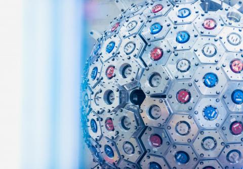
Caption: DESCANT (at TRIUMF) neutron detector array composed of 70 hexagonal detectors Credit: Pamela Joe McFarlane
With all those hexagons and a spherical shape, the DESCANT looks like a ‘buckyball’ or buckminsterfullerene or C60 to me.
I hope the next Summit features TRIUMF and/or some other endeavours which exemplify, Science, Technology, and Creativity in British Columbia and Canada.
Onto the last booth,
- MITACS was originally one of the Canadian federal government’s Network Centres for Excellence projects. It was focused on mathematics, networking, and innovation but once the money ran out the organization took a turn. These days, it’s describing itself as (from their About page) “a national, not-for-profit organization that has designed and delivered research and training programs in Canada for 15 years. Working with 60 universities, thousands of companies, and both federal and provincial governments, we build partnerships that support industrial and social innovation in Canada.”Their Jan. 19, 2016 news release (coincidental with the #BCTECH Summit, Jan. 18 – 19, 2016?) features a new report about improving international investment in Canada,”Opportunities to improve Canada’s attractiveness for R&D investment were identified:1.Canada needs to better incentivize R&D by rebalancing direct and indirect support measures
2.Canada requires a coordinated, client-centric approach to incentivizing R&D
3.Canada needs to invest in training programs that grow the knowledge economy”
Oddly, entrepreneurial/corporate/business types never have a problem with government spending when the money is coming to them; it’s only a problem when it’s social services.
Back to MITACS, one of their more interesting (to me) projects was announced at the 2015 Canadian Science Policy Conference. MITACS has inaugurated a Canadian Science Policy Fellowships programme which in its first year (pilot) will see up up to 10 academics applying their expertise to policy-making while embedded in various federal government agencies. I don’t believe anything similar has occurred here in Canada although, if memory serves, the Brits have a similar programme.
Finally, I offer kudos to Sherry Zhao, MITACS Business Development Specialist, the only person to ask me how her organization might benefit my business. Admittedly I didn’t talk to a lot of people but it’s striking to me that at an ‘innovation and business’ tech summit, only one person approached me about doing business. Of course, I’m not a male aged between 25 and 55. So, extra kudos to Sherry Zhao and MITACS.
Christy Clark (Premier of British Columbia), in her opening comments, stated 2800 (they were expecting about 1000) had signed up for the #BCTECH Summit. I haven’t been able to verify that number or get other additional information, e.g., business deals, research breakthroughs, etc. announced at the Summit. Regardless, it was exciting to attend and find out about the latest and greatest on the BC scene.
I wish all the participants great and good luck and look forward to next year’s where perhaps we’ll here about how the province plans to help with the ‘manufacturing middle’ issue. For new products you need to have facilities capable of reproducing your devices at a speed that satisfies your customers; see my Feb. 10, 2014 post featuring a report on this and other similar issues from the US General Accountability Office.
*’BCTECH Summit 2016′ link added Jan. 21, 2016.