Tag Archives: Taimur Ahmed

Using light to manipulate neurons

There are three (or more?) possible applications including neuromorphic computing for this new optoelectronic technology which is based on black phophorus. A July 16, 2019 news item on Nanowerk announces the research,

Researchers from RMIT University [Australia] drew inspiration from an emerging tool in biotechnology – optogenetics – to develop a device that replicates the way the brain stores and loses information.

Optogenetics allows scientists to delve into the body’s electrical system with incredible precision, using light to manipulate neurons so that they can be turned on or off.

The new chip is based on an ultra-thin material that changes electrical resistance in response to different wavelengths of light, enabling it to mimic the way that neurons work to store and delete information in the brain.

Caption: The new chip is based on an ultra-thin material that changes electrical resistance in response to different wavelengths of light. Credit: RMIT University

A July 17, 2019 RMIT University press release (also on EurekAlert but published on July 16, 2019), which originated the news item, expands on the theme,

Research team leader Dr Sumeet Walia said the technology moves us closer towards artificial intelligence (AI) that can harness the brain’s full sophisticated functionality.

“Our optogenetically-inspired chip imitates the fundamental biology of nature’s best computer – the human brain,” Walia said.

“Being able to store, delete and process information is critical for computing, and the brain does this extremely efficiently.

“We’re able to simulate the brain’s neural approach simply by shining different colours onto our chip.

“This technology takes us further on the path towards fast, efficient and secure light-based computing.

“It also brings us an important step closer to the realisation of a bionic brain – a brain-on-a-chip that can learn from its environment just like humans do.”

Dr Taimur Ahmed, lead author of the study published in Advanced Functional Materials, said being able to replicate neural behavior on an artificial chip offered exciting avenues for research across sectors.

“This technology creates tremendous opportunities for researchers to better understand the brain and how it’s affected by disorders that disrupt neural connections, like Alzheimer’s disease and dementia,” Ahmed said.

The researchers, from the Functional Materials and Microsystems Research Group at RMIT, have also demonstrated the chip can perform logic operations – information processing – ticking another box for brain-like functionality.

Developed at RMIT’s MicroNano Research Facility, the technology is compatible with existing electronics and has also been demonstrated on a flexible platform, for integration into wearable electronics.

How the chip works:

Neural connections happen in the brain through electrical impulses. When tiny energy spikes reach a certain threshold of voltage, the neurons bind together – and you’ve started creating a memory.

On the chip, light is used to generate a photocurrent. Switching between colors causes the current to reverse direction from positive to negative.

This direction switch, or polarity shift, is equivalent to the binding and breaking of neural connections, a mechanism that enables neurons to connect (and induce learning) or inhibit (and induce forgetting).

This is akin to optogenetics, where light-induced modification of neurons causes them to either turn on or off, enabling or inhibiting connections to the next neuron in the chain.

To develop the technology, the researchers used a material called black phosphorus (BP) that can be inherently defective in nature.

This is usually a problem for optoelectronics, but with precision engineering the researchers were able to harness the defects to create new functionality.

“Defects are usually looked on as something to be avoided, but here we’re using them to create something novel and useful,” Ahmed said.

“It’s a creative approach to finding solutions for the technical challenges we face.”

Here’s a link and a citation for the paper,

Multifunctional Optoelectronics via Harnessing Defects in Layered Black Phosphorus by Taimur Ahmed, Sruthi Kuriakose, Sherif Abbas,, Michelle J. S. Spencer, Md. Ataur Rahman, Muhammad Tahir, Yuerui Lu, Prashant Sonar, Vipul Bansal, Madhu Bhaskaran, Sharath Sriram, Sumeet Walia. Advanced Functional Materials DOI: https://doi.org/10.1002/adfm.201901991 First published (online): 17 July 2019

This paper is behind a paywall.

Making nanoscale transistor chips out of thin air—sort of

Caption: The nano-gap transistors operating in air. As gaps become smaller than the mean-free path of electrons in air, there is ballistic electron transport. Credit: RMIT University

A November 19, 2018 news item on Nanowerk describes the ‘airy’ work ( Note: A link has been removed),

Researchers at RMIT University [Ausralia] have engineered a new type of transistor, the building block for all electronics. Instead of sending electrical currents through silicon, these transistors send electrons through narrow air gaps, where they can travel unimpeded as if in space.

The device unveiled in material sciences journal Nano Letters (“Metal–Air Transistors: Semiconductor-free field-emission air-channel nanoelectronics”), eliminates the use of any semiconductor at all, making it faster and less prone to heating up.

A November 19, 2018 RMIT University news release on EurkeAlert, which originated the news item, describes the work and possibilities in more detail,

Lead author and PhD candidate in RMIT’s Functional Materials and Microsystems Research Group, Ms Shruti Nirantar, said this promising proof-of-concept design for nanochips as a combination of metal and air gaps could revolutionise electronics.

“Every computer and phone has millions to billions of electronic transistors made from silicon, but this technology is reaching its physical limits where the silicon atoms get in the way of the current flow, limiting speed and causing heat,” Nirantar said.

“Our air channel transistor technology has the current flowing through air, so there are no collisions to slow it down and no resistance in the material to produce heat.”

The power of computer chips – or number of transistors squeezed onto a silicon chip – has increased on a predictable path for decades, roughly doubling every two years. But this rate of progress, known as Moore’s Law, has slowed in recent years as engineers struggle to make transistor parts, which are already smaller than the tiniest viruses, smaller still.

Nirantar says their research is a promising way forward for nano electronics in response to the limitation of silicon-based electronics.

“This technology simply takes a different pathway to the miniaturisation of a transistor in an effort to uphold Moore’s Law for several more decades,” Shruti said.

Research team leader Associate Professor Sharath Sriram said the design solved a major flaw in traditional solid channel transistors – they are packed with atoms – which meant electrons passing through them collided, slowed down and wasted energy as heat.

“Imagine walking on a densely crowded street in an effort to get from point A to B. The crowd slows your progress and drains your energy,” Sriram said.

“Travelling in a vacuum on the other hand is like an empty highway where you can drive faster with higher energy efficiency.”

But while this concept is obvious, vacuum packaging solutions around transistors to make them faster would also make them much bigger, so are not viable.

“We address this by creating a nanoscale gap between two metal points. The gap is only a few tens of nanometers, or 50,000 times smaller than the width of a human hair, but it’s enough to fool electrons into thinking that they are travelling through a vacuum and re-create a virtual outer-space for electrons within the nanoscale air gap,” he said.

The nanoscale device is designed to be compatible with modern industry fabrication and development processes. It also has applications in space – both as electronics resistant to radiation and to use electron emission for steering and positioning ‘nano-satellites’.

“This is a step towards an exciting technology which aims to create something out of nothing to significantly increase speed of electronics and maintain pace of rapid technological progress,” Sriram said.

Here’s a link to and a citation for the paper,

Metal–Air Transistors: Semiconductor-free field-emission air-channel nanoelectronics by
Shruti Nirantar, Taimur Ahmed, Guanghui Ren, Philipp Gutruf, Chenglong Xu, Madhu Bhaskaran, Sumeet Walia, and Sharath Sriram. Nano Lett., DOI: 10.1021/acs.nanolett.8b02849 Publication Date (Web): November 16, 2018

Copyright © 2018 American Chemical Society

This paper is behind a paywall.

An artificial enzyme uses light to kill bacteria

An April 4, 2018 news item on ScienceDaily announces a light-based approach to killing bacteria,

Researchers from RMIT University [Australia] have developed a new artificial enzyme that uses light to kill bacteria.

The artificial enzymes could one day be used in the fight against infections, and to keep high-risk public spaces like hospitals free of bacteria like E. coli and Golden Staph.

E. coli can cause dysentery and gastroenteritis, while Golden Staph is the major cause of hospital-acquired secondary infections and chronic wound infections.

Made from tiny nanorods — 1000 times smaller than the thickness of the human hair — the “NanoZymes” use visible light to create highly reactive oxygen species that rapidly break down and kill bacteria.

Lead researcher, Professor Vipul Bansal who is an Australian Future Fellow and Director of RMIT’s Sir Ian Potter NanoBioSensing Facility, said the new NanoZymes offer a major cutting edge over nature’s ability to kill bacteria.

Dead bacteria made beautiful,

Caption: A 3-D rendering of dead bacteria after it has come into contact with the NanoZymes.
Credit: Dr. Chaitali Dekiwadia/ RMIT Microscopy and Microanalysis Facility

An April 5, 2018 RMIT University press release (also on EurekAlert but dated April 4, 2018), which originated the news item, expands on the theme,

“For a number of years we have been attempting to develop artificial enzymes that can fight bacteria, while also offering opportunities to control bacterial infections using external ‘triggers’ and ‘stimuli’,” Bansal said. “Now we have finally cracked it.

“Our NanoZymes are artificial enzymes that combine light with moisture to cause a biochemical reaction that produces OH radicals and breaks down bacteria. Nature’s antibacterial activity does not respond to external triggers such as light.

“We have shown that when shined upon with a flash of white light, the activity of our NanoZymes increases by over 20 times, forming holes in bacterial cells and killing them efficiently.

“This next generation of nanomaterials are likely to offer new opportunities in bacteria free surfaces and controlling spread of infections in public hospitals.”

The NanoZymes work in a solution that mimics the fluid in a wound. This solution could be sprayed onto surfaces.

The NanoZymes are also produced as powders to mix with paints, ceramics and other consumer products. This could mean bacteria-free walls and surfaces in hospitals.

Public toilets — places with high levels of bacteria, and in particular E. coli — are also a prime location for the NanoZymes, and the researchers believe their new technology may even have the potential to create self-cleaning toilet bowls.

While the NanoZymes currently use visible light from torches or similar light sources, in the future they could be activated by sunlight.

The researchers have shown that the NanoZymes work in a lab environment. The team is now evaluating the long-term performance of the NanoZymes in consumer products.

“The next step will be to validate the bacteria killing and wound healing ability of these NanoZymes outside of the lab,” Bansal said.

“This NanoZyme technology has huge potential, and we are seeking interest from appropriate industries for joint product development.”

Here’s a link to and a citation for the paper,

Visible-Light-Triggered Reactive-Oxygen-Species-Mediated Antibacterial Activity of Peroxidase-Mimic CuO Nanorods by Md. Nurul Karim, Mandeep Singh, Pabudi Weerathunge, Pengju Bian, Rongkun Zheng, Chaitali Dekiwadia, Taimur Ahmed, Sumeet Walia, Enrico Della Gaspera, Sanjay Singh, Rajesh Ramanathan, and Vipul Bansal. ACS Appl. Nano Mater., Article ASAP DOI: 10.1021/acsanm.8b00153 Publication Date (Web): March 6, 2018

Copyright © 2018 American Chemical Society

This paper is open access.

‘Smart’ windows from Australia

My obsession with smart windows has been lying dormant until now. This February 25, 2018 RMIT University (Australia) press release on EurekAlert has reawkened it,

Researchers from RMIT University in Melbourne Australia have developed a new ultra-thin coating that responds to heat and cold, opening the door to “smart windows”.

The self-modifying coating, which is a thousand times thinner than a human hair, works by automatically letting in more heat when it’s cold and blocking the sun’s rays when it’s hot.

Smart windows have the ability to naturally regulate temperatures inside a building, leading to major environmental benefits and significant financial savings.

Lead investigator Associate Professor Madhu Bhaskaran said the breakthrough will help meet future energy needs and create temperature-responsive buildings.

“We are making it possible to manufacture smart windows that block heat during summer and retain heat inside when the weather cools,” Bhaskaran said.

“We lose most of our energy in buildings through windows. This makes maintaining buildings at a certain temperature a very wasteful and unavoidable process.

“Our technology will potentially cut the rising costs of air-conditioning and heating, as well as dramatically reduce the carbon footprint of buildings of all sizes.

“Solutions to our energy crisis do not come only from using renewables; smarter technology that eliminates energy waste is absolutely vital.”

Smart glass windows are about 70 per cent more energy efficient during summer and 45 per cent more efficient in the winter compared to standard dual-pane glass.

New York’s Empire State Building reported energy savings of US$2.4 million and cut carbon emissions by 4,000 metric tonnes after installing smart glass windows. This was using a less effective form of technology.

“The Empire State Building used glass that still required some energy to operate,” Bhaskaran said. “Our coating doesn’t require energy and responds directly to changes in temperature.”

Co-researcher and PhD student Mohammad Taha said that while the coating reacts to temperature it can also be overridden with a simple switch.

“This switch is similar to a dimmer and can be used to control the level of transparency on the window and therefore the intensity of lighting in a room,” Taha said. “This means users have total freedom to operate the smart windows on-demand.”

Windows aren’t the only clear winners when it comes to the new coating. The technology can also be used to control non-harmful radiation that can penetrate plastics and fabrics. This could be applied to medical imaging and security scans.

Bhaskaran said that the team was looking to roll the technology out as soon as possible.

“The materials and technology are readily scalable to large area surfaces, with the underlying technology filed as a patent in Australia and the US,” she said.

The research has been carried out at RMIT University’s state-of-the-art Micro Nano Research Facility with colleagues at the University of Adelaide and supported by the Australian Research Council.

How the coating works

The self-regulating coating is created using a material called vanadium dioxide. The coating is 50-150 nanometres in thickness.

At 67 degrees Celsius, vanadium dioxide transforms from being an insulator into a metal, allowing the coating to turn into a versatile optoelectronic material controlled by and sensitive to light.

The coating stays transparent and clear to the human eye but goes opaque to infra-red solar radiation, which humans cannot see and is what causes sun-induced heating.

Until now, it has been impossible to use vanadium dioxide on surfaces of various sizes because the placement of the coating requires the creation of specialised layers, or platforms.

The RMIT researchers have developed a way to create and deposit the ultra-thin coating without the need for these special platforms – meaning it can be directly applied to surfaces like glass windows.

Here’s a link to and a citation for the paper,

Insulator–metal transition in substrate-independent VO2 thin film for phase-change device by Mohammad Taha, Sumeet Walia, Taimur Ahmed, Daniel Headland, Withawat Withayachumnankul, Sharath Sriram, & Madhu Bhaskaran. Scientific Reportsvolume 7, Article number: 17899 (2017) doi:10.1038/s41598-017-17937-3 Published online: 20 December 2017

This paper is open access.

For anyone interested in more ‘smart’ windows, you can try that search term or ‘electrochromic’, ‘photochromic’, and ‘thermochromic’ , as well.

Memristor, memristor, you are popular

Regular readers know I have a long-standing interest in memristor and artificial brains. I have three memristor-related pieces of research,  published in the last month or so, for this post.

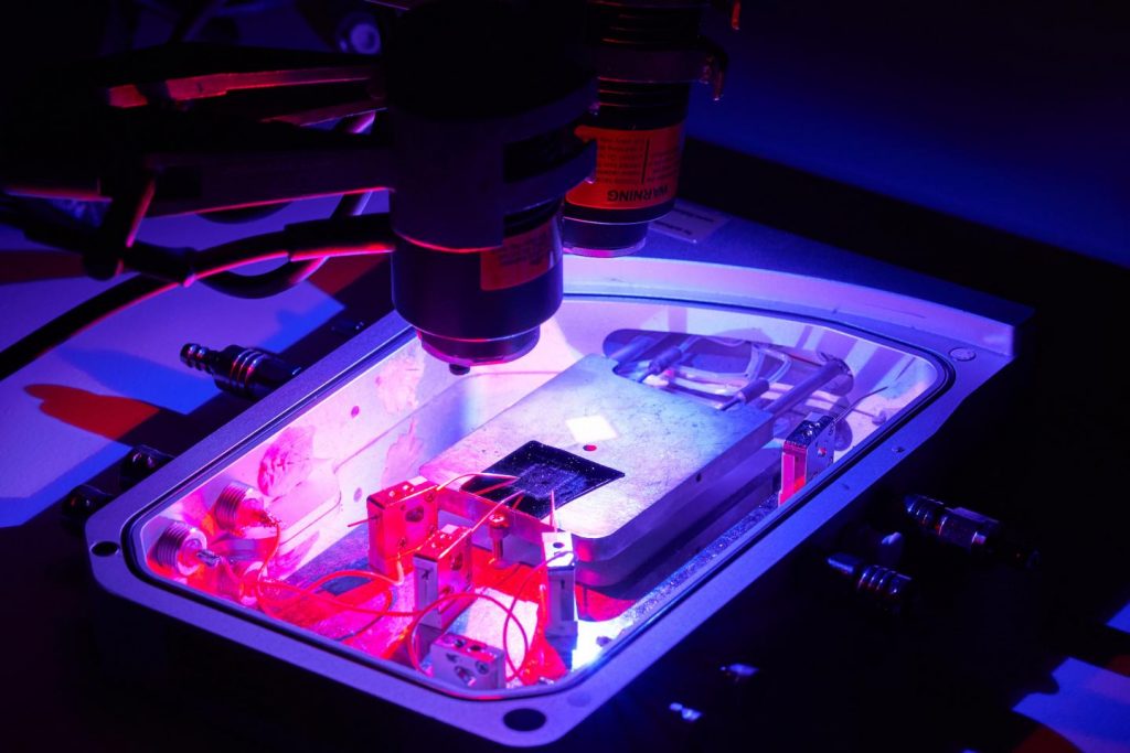
First, there’s some research into nano memory at RMIT University, Australia, and the University of California at Santa Barbara (UC Santa Barbara). From a May 12, 2015 news item on ScienceDaily,

RMIT University researchers have mimicked the way the human brain processes information with the development of an electronic long-term memory cell.

Researchers at the MicroNano Research Facility (MNRF) have built the one of the world’s first electronic multi-state memory cell which mirrors the brain’s ability to simultaneously process and store multiple strands of information.

The development brings them closer to imitating key electronic aspects of the human brain — a vital step towards creating a bionic brain — which could help unlock successful treatments for common neurological conditions such as Alzheimer’s and Parkinson’s diseases.

A May 11, 2015 RMIT University news release, which originated the news item, reveals more about the researchers’ excitement and about the research,

“This is the closest we have come to creating a brain-like system with memory that learns and stores analog information and is quick at retrieving this stored information,” Dr Sharath said.

“The human brain is an extremely complex analog computer… its evolution is based on its previous experiences, and up until now this functionality has not been able to be adequately reproduced with digital technology.”

The ability to create highly dense and ultra-fast analog memory cells paves the way for imitating highly sophisticated biological neural networks, he said.

The research builds on RMIT’s previous discovery where ultra-fast nano-scale memories were developed using a functional oxide material in the form of an ultra-thin film – 10,000 times thinner than a human hair.

Dr Hussein Nili, lead author of the study, said: “This new discovery is significant as it allows the multi-state cell to store and process information in the very same way that the brain does.

“Think of an old camera which could only take pictures in black and white. The same analogy applies here, rather than just black and white memories we now have memories in full color with shade, light and texture, it is a major step.”

While these new devices are able to store much more information than conventional digital memories (which store just 0s and 1s), it is their brain-like ability to remember and retain previous information that is exciting.

“We have now introduced controlled faults or defects in the oxide material along with the addition of metallic atoms, which unleashes the full potential of the ‘memristive’ effect – where the memory element’s behaviour is dependent on its past experiences,” Dr Nili said.

Nano-scale memories are precursors to the storage components of the complex artificial intelligence network needed to develop a bionic brain.

Dr Nili said the research had myriad practical applications including the potential for scientists to replicate the human brain outside of the body.

“If you could replicate a brain outside the body, it would minimise ethical issues involved in treating and experimenting on the brain which can lead to better understanding of neurological conditions,” Dr Nili said.

The research, supported by the Australian Research Council, was conducted in collaboration with the University of California Santa Barbara.

Here’s a link to and a citation for this memristive nano device,

Donor-Induced Performance Tuning of Amorphous SrTiO3 Memristive Nanodevices: Multistate Resistive Switching and Mechanical Tunability by  Hussein Nili, Sumeet Walia, Ahmad Esmaielzadeh Kandjani, Rajesh Ramanathan, Philipp Gutruf, Taimur Ahmed, Sivacarendran Balendhran, Vipul Bansal, Dmitri B. Strukov, Omid Kavehei, Madhu Bhaskaran, and Sharath Sriram. Advanced Functional Materials DOI: 10.1002/adfm.201501019 Article first published online: 14 APR 2015

© 2015 WILEY-VCH Verlag GmbH & Co. KGaA, Weinheim

This paper is behind a paywall.

The second published piece of memristor-related research comes from a UC Santa Barbara and  Stony Brook University (New York state) team but is being publicized by UC Santa Barbara. From a May 11, 2015 news item on Nanowerk (Note: A link has been removed),

In what marks a significant step forward for artificial intelligence, researchers at UC Santa Barbara have demonstrated the functionality of a simple artificial neural circuit (Nature, “Training and operation of an integrated neuromorphic network based on metal-oxide memristors”). For the first time, a circuit of about 100 artificial synapses was proved to perform a simple version of a typical human task: image classification.

A May 11, 2015 UC Santa Barbara news release (also on EurekAlert)by Sonia Fernandez, which originated the news item, situates this development within the ‘artificial brain’ effort while describing it in more detail (Note: A link has been removed),

“It’s a small, but important step,” said Dmitri Strukov, a professor of electrical and computer engineering. With time and further progress, the circuitry may eventually be expanded and scaled to approach something like the human brain’s, which has 1015 (one quadrillion) synaptic connections.

For all its errors and potential for faultiness, the human brain remains a model of computational power and efficiency for engineers like Strukov and his colleagues, Mirko Prezioso, Farnood Merrikh-Bayat, Brian Hoskins and Gina Adam. That’s because the brain can accomplish certain functions in a fraction of a second what computers would require far more time and energy to perform.

… As you read this, your brain is making countless split-second decisions about the letters and symbols you see, classifying their shapes and relative positions to each other and deriving different levels of meaning through many channels of context, in as little time as it takes you to scan over this print. Change the font, or even the orientation of the letters, and it’s likely you would still be able to read this and derive the same meaning.

In the researchers’ demonstration, the circuit implementing the rudimentary artificial neural network was able to successfully classify three letters (“z”, “v” and “n”) by their images, each letter stylized in different ways or saturated with “noise”. In a process similar to how we humans pick our friends out from a crowd, or find the right key from a ring of similar keys, the simple neural circuitry was able to correctly classify the simple images.

“While the circuit was very small compared to practical networks, it is big enough to prove the concept of practicality,” said Merrikh-Bayat. According to Gina Adam, as interest grows in the technology, so will research momentum.

“And, as more solutions to the technological challenges are proposed the technology will be able to make it to the market sooner,” she said.

Key to this technology is the memristor (a combination of “memory” and “resistor”), an electronic component whose resistance changes depending on the direction of the flow of the electrical charge. Unlike conventional transistors, which rely on the drift and diffusion of electrons and their holes through semiconducting material, memristor operation is based on ionic movement, similar to the way human neural cells generate neural electrical signals.

“The memory state is stored as a specific concentration profile of defects that can be moved back and forth within the memristor,” said Strukov. The ionic memory mechanism brings several advantages over purely electron-based memories, which makes it very attractive for artificial neural network implementation, he added.

“For example, many different configurations of ionic profiles result in a continuum of memory states and hence analog memory functionality,” he said. “Ions are also much heavier than electrons and do not tunnel easily, which permits aggressive scaling of memristors without sacrificing analog properties.”

This is where analog memory trumps digital memory: In order to create the same human brain-type functionality with conventional technology, the resulting device would have to be enormous — loaded with multitudes of transistors that would require far more energy.

“Classical computers will always find an ineluctable limit to efficient brain-like computation in their very architecture,” said lead researcher Prezioso. “This memristor-based technology relies on a completely different way inspired by biological brain to carry on computation.”

To be able to approach functionality of the human brain, however, many more memristors would be required to build more complex neural networks to do the same kinds of things we can do with barely any effort and energy, such as identify different versions of the same thing or infer the presence or identity of an object not based on the object itself but on other things in a scene.

Potential applications already exist for this emerging technology, such as medical imaging, the improvement of navigation systems or even for searches based on images rather than on text. The energy-efficient compact circuitry the researchers are striving to create would also go a long way toward creating the kind of high-performance computers and memory storage devices users will continue to seek long after the proliferation of digital transistors predicted by Moore’s Law becomes too unwieldy for conventional electronics.

Here’s a link to and a citation for the paper,

Training and operation of an integrated neuromorphic network based on metal-oxide memristors by M. Prezioso, F. Merrikh-Bayat, B. D. Hoskins, G. C. Adam, K. K. Likharev,    & D. B. Strukov. Nature 521, 61–64 (07 May 2015) doi:10.1038/nature14441

This paper is behind a paywall but a free preview is available through ReadCube Access.

The third and last piece of research, which is from Rice University, hasn’t received any publicity yet, unusual given Rice’s very active communications/media department. Here’s a link to and a citation for their memristor paper,

2D materials: Memristor goes two-dimensional by Jiangtan Yuan & Jun Lou. Nature Nanotechnology 10, 389–390 (2015) doi:10.1038/nnano.2015.94 Published online 07 May 2015

This paper is behind a paywall but a free preview is available through ReadCube Access.

Dexter Johnson has written up the RMIT research (his May 14, 2015 post on the Nanoclast blog on the IEEE [Institute of Electrical and Electronics Engineers] website). He linked it to research from Mark Hersam’s team at Northwestern University (my April 10, 2015 posting) on creating a three-terminal memristor enabling its use in complex electronics systems. Dexter strongly hints in his headline that these developments could lead to bionic brains.

For those who’d like more memristor information, this June 26, 2014 posting which brings together some developments at the University of Michigan and information about developments in the industrial sector is my suggestion for a starting point. Also, you may want to check out my material on HP Labs, especially prominent in the story due to the company’s 2008 ‘discovery’ of the memristor, described on a page in my Nanotech Mysteries wiki, and the controversy triggered by the company’s terminology (there’s more about the controversy in my April 7, 2010 interview with Forrest H Bennett III).