Tag Archives: Takao Someya

Nanomesh for hypoallergenic wearable electronics

It stands to reason that sensors and monitoring devices held against the skin (wearable electronics) for long periods of time could provoke an allergic reaction. Scientists at the University of Tokyo have devised a possible solution according to a July 17, 2017 news item on ScienceDaily,

A hypoallergenic electronic sensor can be worn on the skin continuously for a week without discomfort, and is so light and thin that users forget they even have it on, says a Japanese group of scientists. The elastic electrode constructed of breathable nanoscale meshes holds promise for the development of noninvasive e-skin devices that can monitor a person’s health continuously over a long period.

Here’s an image illustrating the hypoallergenic electronics,

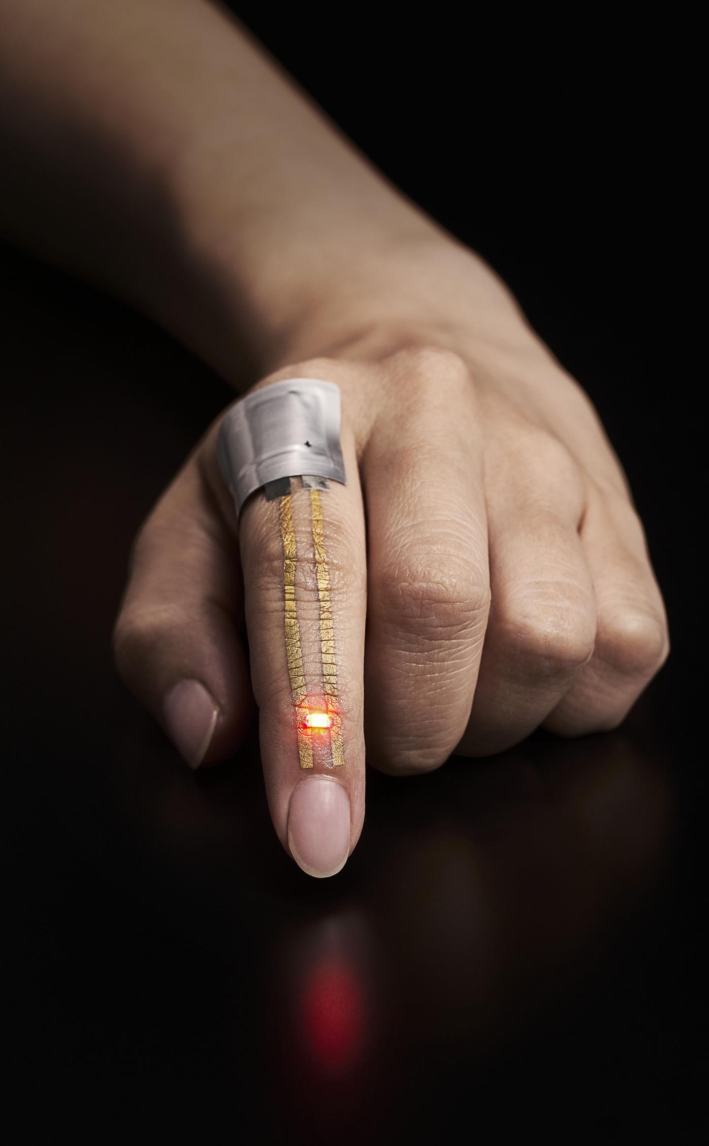
Caption: The electric current from a flexible battery placed near the knuckle flows through the conductor and powers the LED just below the fingernail. Credit: 2017 Someya Laboratory.

A University of Tokyo press release on EurekAlert, which originated the news item, expands on the theme,

Wearable electronics that monitor heart rate and other vital health signals have made headway in recent years, with next-generation gadgets employing lightweight, highly elastic materials attached directly onto the skin for more sensitive, precise measurements. However, although the ultrathin films and rubber sheets used in these devices adhere and conform well to the skin, their lack of breathability is deemed unsafe for long-term use: dermatological tests show the fine, stretchable materials prevent sweating and block airflow around the skin, causing irritation and inflammation, which ultimately could lead to lasting physiological and psychological effects.

“We learned that devices that can be worn for a week or longer for continuous monitoring were needed for practical use in medical and sports applications,” says Professor Takao Someya at the University of Tokyo’s Graduate School of Engineering whose research group had previously developed an on-skin patch that measured oxygen in blood.

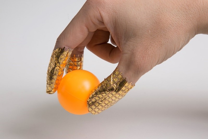
In the current research, the group developed an electrode constructed from nanoscale meshes containing a water-soluble polymer, polyvinyl alcohol (PVA), and a gold layer–materials considered safe and biologically compatible with the body. The device can be applied by spraying a tiny amount of water, which dissolves the PVA nanofibers and allows it to stick easily to the skin–it conformed seamlessly to curvilinear surfaces of human skin, such as sweat pores and the ridges of an index finger’s fingerprint pattern.

The researchers next conducted a skin patch test on 20 subjects and detected no inflammation on the participants’ skin after they had worn the device for a week. The group also evaluated the permeability, with water vapor, of the nanomesh conductor–along with those of other substrates like ultrathin plastic foil and a thin rubber sheet–and found that its porous mesh structure exhibited superior gas permeability compared to that of the other materials.

Furthermore, the scientists proved the device’s mechanical durability through repeated bending and stretching, exceeding 10,000 times, of a conductor attached on the forefinger; they also established its reliability as an electrode for electromyogram recordings when its readings of the electrical activity of muscles were comparable to those obtained through conventional gel electrodes.

“It will become possible to monitor patients’ vital signs without causing any stress or discomfort,” says Someya about the future implications of the team’s research. In addition to nursing care and medical applications, the new device promises to enable continuous, precise monitoring of athletes’ physiological signals and bodily motion without impeding their training or performance.

Here’s a link to and a citation for the paper,

Inflammation-free, gas-permeable, lightweight, stretchable on-skin electronics with nanomeshes by Akihito Miyamoto, Sungwon Lee, Nawalage Florence Cooray, Sunghoon Lee, Mami Mori, Naoji Matsuhisa, Hanbit Jin, Leona Yoda, Tomoyuki Yokota, Akira Itoh, Masaki Sekino, Hiroshi Kawasaki, Tamotsu Ebihara, Masayuki Amagai, & Takao Someya. Nature Nanotechnology (2017) doi:10.1038/nnano.2017.125 Published online 17 July 2017

This paper is behind a paywall.

Fingertip pressure sensors from Japan

Pressure sensor The pressure sensors wraps around and conforms to the shape of the fingers while still accurately measuring pressure distribution. © 2016 Someya Laboratory.

Pressure sensor
The pressure sensors wraps around and conforms to the shape of the fingers while still accurately measuring pressure distribution.
© 2016 Someya Laboratory.

Those fingertip sensors could be jewellery but they’re not. From a March 8, 2016 news item on Nanowerk (Note: A link has been removed),

Researchers at the University of Tokyo working with American colleagues have developed a transparent, bendable and sensitive pressure sensor (“A Transparent, Bending Insensitive Pressure Sensor”). Healthcare practitioners may one day be able to physically screen for breast cancer using pressure-sensitive rubber gloves to detect tumors, owing to this newly developed sensor.

A March 7, 2016 University of Tokyo press release, which originated the news item, expands on the theme,

Conventional pressure sensors are flexible enough to fit to soft surfaces such as human skin, but they cannot measure pressure changes accurately once they are twisted or wrinkled, making them unsuitable for use on complex and moving surfaces. Additionally, it is difficult to reduce them below 100 micrometers thickness because of limitations in current production methods.

To address these issues, an international team of researchers led by Dr. Sungwon Lee and Professor Takao Someya of the University of Tokyo’s Graduate School of Engineering has developed a nanofiber-type pressure sensor that can measure pressure distribution of rounded surfaces such as an inflated balloon and maintain its sensing accuracy even when bent over a radius of 80 micrometers, equivalent to just twice the width of a human hair. The sensor is roughly 8 micrometers thick and can measure the pressure in 144 locations at once.

The device demonstrated in this study consists of organic transistors, electronic switches made from carbon and oxygen based organic materials, and a pressure sensitive nanofiber structure. Carbon nanotubes and graphene were added to an elastic polymer to create nanofibers with a diameter of 300 to 700 nanometers, which were then entangled with each other to form a transparent, thin and light porous structure.

“We’ve also tested the performance of our pressure sensor with an artificial blood vessel and found that it could detect small pressure changes and speed of pressure propagation,” says Lee. He continues, “Flexible electronics have great potential for implantable and wearable devices. I realized that many groups are developing flexible sensors that can measure pressure but none of them are suitable for measuring real objects since they are sensitive to distortion. That was my main motivation and I think we have proposed an effective solution to this problem.”

Here’s a link to and a citation for the paper,

A transparent bending-insensitive pressure sensor by Sungwon Lee, Amir Reuveny, Jonathan Reeder, Sunghoon Lee, Hanbit Jin, Qihan Liu, Tomoyuki Yokota, Tsuyoshi Sekitani, Takashi Isoyama, Yusuke Abe, Zhigang Suo & Takao Someya. Nature Nanotechnology (2016)  doi:10.1038/nnano.2015.324 Published online 25 January 2016

This paper is behind a paywall.

Institute for Electrical and Electronics Engineers’ (IEEE) Nano 2015 conference call for papers

The institute for Electrical and Electronics Engineers is holding its Nano 2015 conference in Rome, Italy from July 27 – 30, 2015. This is the second call for papers (I missed the first call),

We invite you to submit papers, proposals for tutorials, workshops to the International IEEE Conference on Nanotechnology which will be held in Rome, July 27-30, 2015. (See www.ieeenano15.org). The dead-line for abstract submission is 15th March 2015.

This conference is the 15th edition of the flagship annual event of the IEEE Nanotechnology Council. IEEE NANO 2015 will provide an international forum for the exchange of technical information in a wide variety of branches of Nanotechnology and Nanoscience, through feature tutorials, workshops, track sessions and special sessions; plenary and invited talks from the most renowned scientists and engineers; exhibition of software, hardware, equipment, materials, services and literature. With its fantastic setting in the centre of the Eternal City, at a walking distance from Colosseum and from the most exciting locations of ancient Rome, IEEE NANO 2015 will provide a perfect forum for inspiration, interactions and exchange of ideas.

All accepted papers will be published by IEEE Press, included in IEEE Xplore and Indexed by EI. Selected conference papers will be considered for publication on IEEE Transactions on Nanotechnology.

Important Dates

March 15, 2015:       Tutorial/Workshop Proposal
March 15, 2015:        Abstract Submission
April 15, 2015:           Acceptance Notification

May 15, 2015:            Full Paper Submission
June 1, 2015:              End of early Registration

Topics for contributing papers include but are not limited to:

Nanosensors, Actuators
Smart systems
Nanomaterials
Graphene-Based Materials
Nano-energy, Energy Harvesting
Nanobiology, Nanobiotechnology
Nanomedicine
Nanoelectronics
Nano-optoelectronics
MEMS/NEMS
Nano-optics, Nano-photonics
Nano-electromagnetics, NanoEMC
Nanofabrication, Nanoassemblies
Nanopackaging
Nanorobotics, Nanomanipulation
Nanometrology
Nanocharacterization
Nanofluidics
Nanomagnetics
Multiscale Modeling and Simulation

PLENARY SPEAKERS (See www.ieeenano15.org/program/plenary-speakers)
George Bourianoff, Intel (USA)
Michael Grätzel, EPFL (Switzerland)
Roberto Cingolani, IIT (Italy)
Rodney Ruoff, NIST (Korea)
Takao Someya, Tokyo Univ. (Japan)
Theresa Mayer, Pennsylvania State Univ. (USA)
Zhong Lin Wang, Georgia Tech (USA)

Proposed SPECIAL SESSIONS
1) Graphene
2) Nanoelectromagnetics and Nano-EMC
3) Nanometrology and device characterization
4) Nanotechnology for microwave and THz
5) Memristor
Part 1: Resistive switching: from fundamentals to production
Part 2: Memristive nanodevices and nanocircuits
6) Nanophononics
7) Drug Toxicity Mitigation. Nanotechnology-Enabled Strategies
8) Conformable Electronics and E-Skin
9) Organic Neurooptoelectronics

There are more details about the call in this PDF. Good luck!