Tag Archives: Technical University of Munich

400 nm thick glucose fuel cell uses body’s own sugar

This May 12, 2022 news item on Nanowerk reminds me of bioenergy harvesting (using the body’s own processes rather than batteries to power implants),

Glucose is the sugar we absorb from the foods we eat. It is the fuel that powers every cell in our bodies. Could glucose also power tomorrow’s medical implants?

Engineers at MIT [Massachusetts Institute of Technology] and the Technical University of Munich think so. They have designed a new kind of glucose fuel cell that converts glucose directly into electricity. The device is smaller than other proposed glucose fuel cells, measuring just 400 nanometers thick. The sugary power source generates about 43 microwatts per square centimeter of electricity, achieving the highest power density of any glucose fuel cell to date under ambient conditions.

Caption: Silicon chip with 30 individual glucose micro fuel cells, seen as small silver squares inside each gray rectangle. Credit Image: Kent Dayton

A May 12, 2022 MIT news release (also on EuekAlert) by Jennifer Chu, which originated the news item, describes the technology in more detail, Note: A link has been removed,

The new device is also resilient, able to withstand temperatures up to 600 degrees Celsius. If incorporated into a medical implant, the fuel cell could remain stable through the high-temperature sterilization process required for all implantable devices.

The heart of the new device is made from ceramic, a material that retains its electrochemical properties even at high temperatures and miniature scales. The researchers envision the new design could be made into ultrathin films or coatings and wrapped around implants to passively power electronics, using the body’s abundant glucose supply.

“Glucose is everywhere in the body, and the idea is to harvest this readily available energy and use it to power implantable devices,” says Philipp Simons, who developed the design as part of his PhD thesis in MIT’s Department of Materials Science and Engineering (DMSE). “In our work we show a new glucose fuel cell electrochemistry.”

“Instead of using a battery, which can take up 90 percent of an implant’s volume, you could make a device with a thin film, and you’d have a power source with no volumetric footprint,” says Jennifer L.M. Rupp, Simons’ thesis supervisor and a DMSE visiting professor, who is also an associate professor of solid-state electrolyte chemistry at Technical University Munich in Germany.

Simons and his colleagues detail their design today in the journal Advanced Materials. Co-authors of the study include Rupp, Steven Schenk, Marco Gysel, and Lorenz Olbrich.

A “hard” separation

The inspiration for the new fuel cell came in 2016, when Rupp, who specializes in ceramics and electrochemical devices, went to take a routine glucose test toward the end of her pregnancy.

“In the doctor’s office, I was a very bored electrochemist, thinking what you could do with sugar and electrochemistry,” Rupp recalls. “Then I realized, it would be good to have a glucose-powered solid state device. And Philipp and I met over coffee and wrote out on a napkin the first drawings.”

The team is not the first to conceive of a glucose fuel cell, which was initially introduced in the 1960s and showed potential for converting glucose’s chemical energy into electrical energy. But glucose fuel cells at the time were based on soft polymers and were quickly eclipsed by lithium-iodide batteries, which would become the standard power source for medical implants, most notably the cardiac pacemaker.

However, batteries have a limit to how small they can be made, as their design requires the physical capacity to store energy.

“Fuel cells directly convert energy rather than storing it in a device, so you don’t need all that volume that’s required to store energy in a battery,” Rupp says.

In recent years, scientists have taken another look at glucose fuel cells as potentially smaller power sources, fueled directly by the body’s abundant glucose.

A glucose fuel cell’s basic design consists of three layers: a top anode, a middle electrolyte, and a bottom cathode. The anode reacts with glucose in bodily fluids, transforming the sugar into gluconic acid. This electrochemical conversion releases a pair of protons and a pair of electrons. The middle electrolyte acts to separate the protons from the electrons, conducting the protons through the fuel cell, where they combine with air to form molecules of water — a harmless byproduct that flows away with the body’s fluid. Meanwhile, the isolated electrons flow to an external circuit, where they can be used to power an electronic device.

The team looked to improve on existing materials and designs by modifying the electrolyte layer, which is often made from polymers. But polymer properties, along with their ability to conduct protons, easily degrade at high temperatures, are difficult to retain when scaled down to the dimension of nanometers, and are hard to sterilize. The researchers wondered if a ceramic — a heat-resistant material which can naturally conduct protons — could be made into an electrolyte for glucose fuel cells.

“When you think of ceramics for such a glucose fuel cell, they have the advantage of long-term stability, small scalability, and silicon chip integration,” Rupp notes. “They’re hard and robust.”

Peak power

The researchers designed a glucose fuel cell with an electrolyte made from ceria, a ceramic material that possesses high ion conductivity, is mechanically robust, and as such, is widely used as an electrolyte in hydrogen fuel cells. It has also been shown to be biocompatible.

“Ceria is actively studied in the cancer research community,” Simons notes. “It’s also similar to zirconia, which is used in tooth implants, and is biocompatible and safe.”

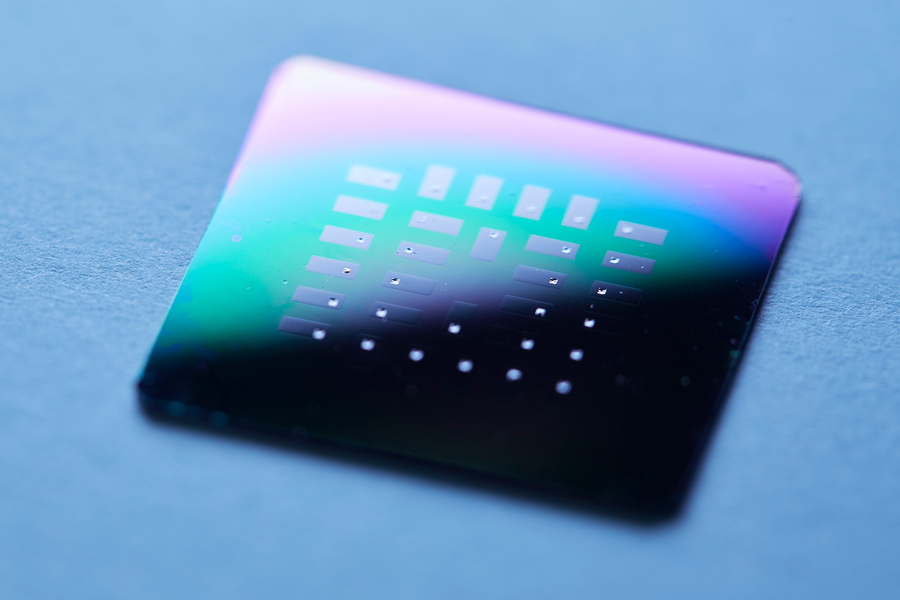
The team sandwiched the electrolyte with an anode and cathode made of platinum, a stable material that readily reacts with glucose. They fabricated 150 individual glucose fuel cells on a chip, each about 400 nanometers thin, and about 300 micrometers wide (about the width of 30 human hairs). They patterned the cells onto silicon wafers, showing that the devices can be paired with a common semiconductor material. They then measured the current produced by each cell as they flowed a solution of glucose over each wafer in a custom-fabricated test station.

They found many cells produced a peak voltage of about 80 millivolts. Given the tiny size of each cell, this output is the highest power density of any existing glucose fuel cell design.

“Excitingly, we are able to draw power and current that’s sufficient to power implantable devices,” Simons says.

“It is the first time that proton conduction in electroceramic materials can be used for glucose-to-power conversion, defining a new type of electrochemstry,” Rupp says. “It extends the material use-cases from hydrogen fuel cells to new, exciting glucose-conversion modes.”

Here’s a link to and a citation for the paper,

A Ceramic-Electrolyte Glucose Fuel Cell for Implantable Electronics by Philipp Simons, Steven A. Schenk, Marco A. Gysel, Lorenz F. Olbrich, Jennifer L. M. Rupp. Advanced Materials https://doi.org/10.1002/adma.202109075 First published: 05 April 2022

This paper is open access.

Reliable findings on the presence of synthetic (engineered) nanoparticles in bodies of water

An Aug. 29, 2016 news item on Nanowerk announces research into determining the presence of engineered (synthetic) nanoparticles in bodies of water,

For a number of years now, an increasing number of synthetic nanoparticles have been manufactured and incorporated into various products, such as cosmetics. For the first time, a research project at the Technical University of Munich and the Bavarian Ministry of the Environment provides reliable findings on their presence in water bodies.

An Aug. 29, 2016 Technical University of Munich (TUM) press release, which originated the news item, provides more information,

Nanoparticles can improve the properties of materials and products. That is the reason why an increasing number of nanoparticles have been manufactured over the past several years. The worldwide consumption of silver nanoparticles is currently estimated at over 300 metric tons. These nanoparticles have the positive effect of killing bacteria and viruses. Products that are coated with these particles include refrigerators and surgical instruments. Silver nanoparticles can even be found in sportswear. This is because the silver particles can prevent the smell of sweat by killing the bacteria that cause it.

Previously, it was unknown whether and in what concentration these nanoparticles enter the environment and e.g. enter bodies of water. If they do, this poses a problem. That is because the silver nanoparticles are toxic to numerous aquatic organisms, and can upset sensitive ecological balances.

Analytical challenge

In the past, however, nanoparticles have not been easy to detect. That is because they measure only 1 to 100 nanometers across [nanoparticles may be larger than 100nm or smaller than 1nm but the official definitions usually specify up to 100nm although some definitions go up to 1000nm] – a nanometer is a millionth of a millimeter. “In order to know if a toxicological hazard exists, we need to know how many of these particles enter the environment, and in particular bodies of water”, explains Michael Schuster, Professor for Analytical Chemistry at the TU Munich.

This was an analytical challenge for the researchers charged with solving the problem on behalf of the Bavarian Ministry of the Environment. In order to overcome this issue, they used a well-known principle that utilizes the effect of surfactants to separate and concentrate the particles. “Surfactants are also found in washing and cleaning detergents”, explains Schuster. “Basically, what they do is envelop grease and dirt particles in what are called micelles, making it possible for them to float in water.” One side of the surfactant is water-soluble, the other fat-soluble. The fat-soluble ends collect around non-polar, non-water soluble compounds such as grease or around particles, and “trap” them in a micelle. The water-soluble, polar ends of the surfactants, on the other hand, point towards the water molecules, allowing the microscopically small micelle to float in water.

A box of sugar cubes in the Walchensee lake

The researchers applied this principle to the nanoparticles. “When the micelles surrounding the particles are warmed slightly, they start to clump”, explains Schuster. This turns the water cloudy. Using a centrifuge, the surfactants and the nanoparticles trapped in them can then be separated from the water. This procedure is called cloud point extraction. The researchers then use the surfactants that have been separated out in this manner – which contain the particles in an unmodified, but highly concentrated form – to measure how many silver nanoparticles are present. To do this, they use a highly sensitive atomic spectrometer configured to only detect silver. In this manner, concentrations in a range of less than one nanogram per liter can be detected. To put this in perspective, this would be like detecting a box of sugar cubes that had dissolved in the Walchensee lake.

With the help of this analysis procedure, it is possible to gain new insight into the concentration of nanoparticles in drinking and waste water, sewage sludge, rivers, and lakes. In Bavaria, the measurements yielded good news: The concentrations measured in the water bodies were extremely low. In was only in four of the 13 Upper Bavarian lakes examined that the concentration even exceeded the minimum detection limit of 0.2 nanograms per liter. No measured value exceeded 1.3 nanograms per liter. So far, no permissible values have been established for silver nanoparticles.

Representative for watercourses, the Isar river was examined from its source to its mouth at around 30 locations. The concentration of silver nanoparticles was also measured in the inflow and outflow of sewage treatment plants. The findings showed that at least 94 percent of silver nanoparticles are filtered out by the sewage treatment plants.

Unfortunately, the researchers have not published their results.

When an atom more or less makes a big difference

As scientists continue exploring the nanoscale, it seems that finding the number of atoms in your particle makes a difference is no longer so surprising. From a Jan. 28, 2016 news item on ScienceDaily,

Combining experimental investigations and theoretical simulations, researchers have explained why platinum nanoclusters of a specific size range facilitate the hydrogenation reaction used to produce ethane from ethylene. The research offers new insights into the role of cluster shapes in catalyzing reactions at the nanoscale, and could help materials scientists optimize nanocatalysts for a broad class of other reactions.

A Jan. 28, 2016 Georgia Institute of Technology (Georgia Tech) news release (*also on EurekAlert*), which originated the news item, expands on the theme,

At the macro-scale, the conversion of ethylene has long been considered among the reactions insensitive to the structure of the catalyst used. However, by examining reactions catalyzed by platinum clusters containing between 9 and 15 atoms, researchers in Germany and the United States found that at the nanoscale, that’s no longer true. The shape of nanoscale clusters, they found, can dramatically affect reaction efficiency.

While the study investigated only platinum nanoclusters and the ethylene reaction, the fundamental principles may apply to other catalysts and reactions, demonstrating how materials at the very smallest size scales can provide different properties than the same material in bulk quantities. …

“We have re-examined the validity of a very fundamental concept on a very fundamental reaction,” said Uzi Landman, a Regents’ Professor and F.E. Callaway Chair in the School of Physics at the Georgia Institute of Technology. “We found that in the ultra-small catalyst range, on the order of a nanometer in size, old concepts don’t hold. New types of reactivity can occur because of changes in one or two atoms of a cluster at the nanoscale.”

The widely-used conversion process actually involves two separate reactions: (1) dissociation of H2 molecules into single hydrogen atoms, and (2) their addition to the ethylene, which involves conversion of a double bond into a single bond. In addition to producing ethane, the reaction can also take an alternative route that leads to the production of ethylidyne, which poisons the catalyst and prevents further reaction.

The project began with Professor Ueli Heiz and researchers in his group at the Technical University of Munich experimentally examining reaction rates for clusters containing 9, 10, 11, 12 or 13 platinum atoms that had been placed atop a magnesium oxide substrate. The 9-atom nanoclusters failed to produce a significant reaction, while larger clusters catalyzed the ethylene hydrogenation reaction with increasingly better efficiency. The best reaction occurred with 13-atom clusters.

Bokwon Yoon, a research scientist in Georgia Tech’s Center for Computational Materials Science, and Landman, the center’s director, then used large-scale first-principles quantum mechanical simulations to understand how the size of the clusters – and their shape – affected the reactivity. Using their simulations, they discovered that the 9-atom cluster resembled a symmetrical “hut,” while the larger clusters had bulges that served to concentrate electrical charges from the substrate.

“That one atom changes the whole activity of the catalyst,” Landman said. “We found that the extra atom operates like a lightning rod. The distribution of the excess charge from the substrate helps facilitate the reaction. Platinum 9 has a compact shape that doesn’t facilitate the reaction, but adding just one atom changes everything.”

Here’s an illustration featuring the difference between a 9 atom cluster and a 10 atom cluster,

A single atom makes a difference in the catalytic properties of platinum nanoclusters. Shown are platinum 9 (top) and platinum 10 (bottom). (Credit: Uzi Landman, Georgia Tech)

A single atom makes a difference in the catalytic properties of platinum nanoclusters. Shown are platinum 9 (top) and platinum 10 (bottom). (Credit: Uzi Landman, Georgia Tech)

The news release explains why the larger clusters function as catalysts,

Nanoclusters with 13 atoms provided the maximum reactivity because the additional atoms shift the structure in a phenomena Landman calls “fluxionality.” This structural adjustment has also been noted in earlier work of these two research groups, in studies of clusters of gold [emphasis mine] which are used in other catalytic reactions.

“Dynamic fluxionality is the ability of the cluster to distort its structure to accommodate the reactants to actually enhance reactivity,” he explained. “Only very small aggregates of metal can show such behavior, which mimics a biochemical enzyme.”

The simulations showed that catalyst poisoning also varies with cluster size – and temperature. The 10-atom clusters can be poisoned at room temperature, while the 13-atom clusters are poisoned only at higher temperatures, helping to account for their improved reactivity.

“Small really is different,” said Landman. “Once you get into this size regime, the old rules of structure sensitivity and structure insensitivity must be assessed for their continued validity. It’s not a question anymore of surface-to-volume ratio because everything is on the surface in these very small clusters.”

While the project examined only one reaction and one type of catalyst, the principles governing nanoscale catalysis – and the importance of re-examining traditional expectations – likely apply to a broad range of reactions catalyzed by nanoclusters at the smallest size scale. Such nanocatalysts are becoming more attractive as a means of conserving supplies of costly platinum.

“It’s a much richer world at the nanoscale than at the macroscopic scale,” added Landman. “These are very important messages for materials scientists and chemists who wish to design catalysts for new purposes, because the capabilities can be very different.”

Along with the experimental surface characterization and reactivity measurements, the first-principles theoretical simulations provide a unique practical means for examining these structural and electronic issues because the clusters are too small to be seen with sufficient resolution using most electron microscopy techniques or traditional crystallography.

“We have looked at how the number of atoms dictates the geometrical structure of the cluster catalysts on the surface and how this geometrical structure is associated with electronic properties that bring about chemical bonding characteristics that enhance the reactions,” Landman added.

I highlighted the news release’s reference to gold nanoclusters as I have noted the number issue in two April 14, 2015 postings, neither of which featured Georgia Tech, Gold atoms: sometimes they’re a metal and sometimes they’re a molecule and Nature’s patterns reflected in gold nanoparticles.

Here’s a link to and a citation for the ‘platinum catalyst’ paper,

Structure sensitivity in the nonscalable regime explored via catalysed ethylene hydrogenation on supported platinum nanoclusters by Andrew S. Crampton, Marian D. Rötzer, Claron J. Ridge, Florian F. Schweinberger, Ueli Heiz, Bokwon Yoon, & Uzi Landman.  Nature Communications 7, Article number: 10389  doi:10.1038/ncomms10389 Published 28 January 2016

This paper is open access.

*’also on EurekAlert’ added Jan. 29, 2016.

Self-assembly with porphine molecules

A Jan. 12, 2016 American Institute of Physics (AIP) news release by John Arnst (also on EurekAlert but dated Jan. 14, 2016) describes computational research into self-assembling nanodevices based on porphine molecules,

As we continue to shrink electronic components, top-down manufacturing methods begin to approach a physical limit at the nanoscale. Rather than continue to chip away at this limit, one solution of interest involves using the bottom-up self-assembly of molecular building blocks to build nanoscale devices.

Successful self-assembly is an elaborately choreographed dance, in which the attractive and repulsive forces within molecules, between each molecule and its neighbors, and between molecules and the surface that supports them, have to all be taken into account. To better understand the self-assembly process, researchers at the Technical University of Munich have characterized the contributions of all interaction components, such as covalent bonding and van der Waals interactions between molecules and between molecules and a surface.

“In an ideal case, the smallest possible device has the size of a single atom or molecule,” said Katharina Diller, who worked as a postdoctoral researcher in the group of Karsten Reuter at the Technical University of Munich. Reuter and his colleagues present their work this week in The Journal of Chemical Physics, from AIP Publishing.

One such example is a single-porphyrin switch, which occupies a surface area of only one square nanometer. [emphasis mine] The porphine molecule, which was the object of this study, is even smaller than this. Porphyrins are a group of ringed chemical compounds which notably include heme – responsible for transporting oxygen and carbon dioxide in the bloodstream – and chlorophyll. In synthetically-derived applications, porphyrins are studied for their potential uses as sensors, light-sensitive dyes in organic solar cells, and molecular magnets.

The researchers from TU Munich assessed the interactions of the porphyrin molecule 2H-porphine by using density functional theory, a quantum mechanical computational modelling method used to describe the electronic properties of molecules and materials. Their simulations were performed at the high-performance supercomputer SuperMUC at Leibniz-Rechenzentrum in Garching.

The metallic substrates the researchers chose for the porphyrin molecules to assemble on, the close packed single crystal surfaces of copper and silver, are widely used as substrates in surface science. This is due to the densely packed nature of the surfaces, which allow the molecules to exhibit a smooth adsorption environment. Additionally, copper and silver each react differently with porhyrins – the molecule adsorbs more strongly on copper, whereas silver does a better job of keeping the electronic structure of the molecule intact – allowing the researchers to monitor a variety of competing effects for future applications.

In their simulation, porphyrin molecules were placed on a copper or silver slab, which was repeated periodically to simulate an extended surface. After finding the optimal geometry in which the molecules would adsorb on the surface, the researchers altered the size of the metal slab to increase or decrease the distance between molecules, thus simulating different molecular coverages. The computational setup gave them a switch to turn the energy contributions of neighboring molecules on and off, in order to observe the interplay of the individual interactions.

Diller and Reuter, along with colleagues Reinhard Maurer and Moritz Müller, who is first author on the paper, found that the weak long-range van der Waals interactions yielded the largest contribution to the molecule-surface interaction, and showed that the often employed methods to quantify the electronic charges in the system have to be used with caution. Surprisingly, while interactions directly between molecules are negligible, the researcher found indications for surface-mediated molecule-molecule interactions at higher molecular coverages.

“The analysis of the electronic structure and the individual interaction components allows us to better understand the self-assembly of porphine adsorbed on copper and silver, and additionally enables predictions for more complex porphyrine analogues,” Diller said. “These conclusions, however, come without yet considering the effects of atomic motion at finite temperature, which we did not study in this work.”

Here’s a link to and a citation for the paper,

Interfacial charge rearrangement and intermolecular interactions: Density-functional theory study of free-base porphine adsorbed on Ag(111) and Cu(111) by Moritz Müller, Katharina Diller, Reinhard J. Maurer, and Karsten Reuter. J. Chem. Phys. 144, 024701 (2016); http://dx.doi.org/10.1063/1.4938259

This paper appears to be open access.

Finally, the researchers have made this illustrative diagram titled ‘Energy’ available,

Caption: Schematic depiction of different energy terms contributing to the adsorption energy, and charge density difference of 2H-P after adsorption onto Cu(111) at 12.8 Angstrom separation. Credit: M. Müller/TU Munich

Caption: Schematic depiction of different energy terms contributing to the adsorption energy, and charge density difference of 2H-P after adsorption onto Cu(111) at 12.8 Angstrom separation. Credit: M. Müller/TU Munich

Replace silicon with black phosphorus instead of graphene?

I have two black phosphorus pieces. This first piece of research comes out of ‘La belle province’ or, as it’s more usually called, Québec (Canada).

Foundational research on phosphorene

There’s a lot of interest in replacing silicon for a number of reasons and, increasingly, there’s interest in finding an alternative to graphene.

A July 7, 2015 news item on Nanotechnology Now describes a new material for use as transistors,

As scientists continue to hunt for a material that will make it possible to pack more transistors on a chip, new research from McGill University and Université de Montréal adds to evidence that black phosphorus could emerge as a strong candidate.

In a study published today in Nature Communications, the researchers report that when electrons move in a phosphorus transistor, they do so only in two dimensions. The finding suggests that black phosphorus could help engineers surmount one of the big challenges for future electronics: designing energy-efficient transistors.

A July 7, 2015 McGill University news release on EurekAlert, which originated the news item, describes the field of 2D materials and the research into black phosphorus and its 2D version, phosperene (analogous to graphite and graphene),

“Transistors work more efficiently when they are thin, with electrons moving in only two dimensions,” says Thomas Szkopek, an associate professor in McGill’s Department of Electrical and Computer Engineering and senior author of the new study. “Nothing gets thinner than a single layer of atoms.”

In 2004, physicists at the University of Manchester in the U.K. first isolated and explored the remarkable properties of graphene — a one-atom-thick layer of carbon. Since then scientists have rushed to to investigate a range of other two-dimensional materials. One of those is black phosphorus, a form of phosphorus that is similar to graphite and can be separated easily into single atomic layers, known as phosphorene.

Phosphorene has sparked growing interest because it overcomes many of the challenges of using graphene in electronics. Unlike graphene, which acts like a metal, black phosphorus is a natural semiconductor: it can be readily switched on and off.

“To lower the operating voltage of transistors, and thereby reduce the heat they generate, we have to get closer and closer to designing the transistor at the atomic level,” Szkopek says. “The toolbox of the future for transistor designers will require a variety of atomic-layered materials: an ideal semiconductor, an ideal metal, and an ideal dielectric. All three components must be optimized for a well designed transistor. Black phosphorus fills the semiconducting-material role.”

The work resulted from a multidisciplinary collaboration among Szkopek’s nanoelectronics research group, the nanoscience lab of McGill Physics Prof. Guillaume Gervais, and the nanostructures research group of Prof. Richard Martel in Université de Montréal’s Department of Chemistry.

To examine how the electrons move in a phosphorus transistor, the researchers observed them under the influence of a magnetic field in experiments performed at the National High Magnetic Field Laboratory in Tallahassee, FL, the largest and highest-powered magnet laboratory in the world. This research “provides important insights into the fundamental physics that dictate the behavior of black phosphorus,” says Tim Murphy, DC Field Facility Director at the Florida facility.

“What’s surprising in these results is that the electrons are able to be pulled into a sheet of charge which is two-dimensional, even though they occupy a volume that is several atomic layers in thickness,” Szkopek says. That finding is significant because it could potentially facilitate manufacturing the material — though at this point “no one knows how to manufacture this material on a large scale.”

“There is a great emerging interest around the world in black phosphorus,” Szkopek says. “We are still a long way from seeing atomic layer transistors in a commercial product, but we have now moved one step closer.”

Here’s a link to and a citation for the paper,

Two-dimensional magnetotransport in a black phosphorus naked quantum well by V. Tayari, N. Hemsworth, I. Fakih, A. Favron, E. Gaufrès, G. Gervais, R. Martel & T. Szkopek. Nature Communications 6, Article number: 7702 doi:10.1038/ncomms8702 Published 07 July 2015

This is an open access paper.

The second piece of research into black phosphorus is courtesy of an international collaboration.

A phosporene transistor

A July 9, 2015 Technical University of Munich (TUM) press release (also on EurekAlert) describes the formation of a phosphorene transistor made possible by the introduction of arsenic,

Chemists at the Technische Universität München (TUM) have now developed a semiconducting material in which individual phosphorus atoms are replaced by arsenic. In a collaborative international effort, American colleagues have built the first field-effect transistors from the new material.

For many decades silicon has formed the basis of modern electronics. To date silicon technology could provide ever tinier transistors for smaller and smaller devices. But the size of silicon transistors is reaching its physical limit. Also, consumers would like to have flexible devices, devices that can be incorporated into clothing and the likes. However, silicon is hard and brittle. All this has triggered a race for new materials that might one day replace silicon.

Black arsenic phosphorus might be such a material. Like graphene, which consists of a single layer of carbon atoms, it forms extremely thin layers. The array of possible applications ranges from transistors and sensors to mechanically flexible semiconductor devices. Unlike graphene, whose electronic properties are similar to those of metals, black arsenic phosphorus behaves like a semiconductor.

The press release goes on to provide more detail about the collaboration and the research,

A cooperation between the Technical University of Munich and the University of Regensburg on the German side and the University of Southern California (USC) and Yale University in the United States has now, for the first time, produced a field effect transistor made of black arsenic phosphorus. The compounds were synthesized by Marianne Koepf at the laboratory of the research group for Synthesis and Characterization of Innovative Materials at the TUM. The field effect transistors were built and characterized by a group headed by Professor Zhou and Dr. Liu at the Department of Electrical Engineering at USC.

The new technology developed at TUM allows the synthesis of black arsenic phosphorus without high pressure. This requires less energy and is cheaper. The gap between valence and conduction bands can be precisely controlled by adjusting the arsenic concentration. “This allows us to produce materials with previously unattainable electronic and optical properties in an energy window that was hitherto inaccessible,” says Professor Tom Nilges, head of the research group for Synthesis and Characterization of Innovative Materials.

Detectors for infrared

With an arsenic concentration of 83 percent the material exhibits an extremely small band gap of only 0.15 electron volts, making it predestined for sensors which can detect long wavelength infrared radiation. LiDAR (Light Detection and Ranging) sensors operate in this wavelength range, for example. They are used, among other things, as distance sensors in automobiles. Another application is the measurement of dust particles and trace gases in environmental monitoring.

A further interesting aspect of these new, two-dimensional semiconductors is their anisotropic electronic and optical behavior. The material exhibits different characteristics along the x- and y-axes in the same plane. To produce graphene like films the material can be peeled off in ultra thin layers. The thinnest films obtained so far are only two atomic layers thick.

Here’s a link to and a citation for the paper,

Black Arsenic–Phosphorus: Layered Anisotropic Infrared Semiconductors with Highly Tunable Compositions and Properties by Bilu Liu, Marianne Köpf, Ahmad N. Abbas, Xiaomu Wang, Qiushi Guo, Yichen Jia, Fengnian Xia, Richard Weihrich, Frederik Bachhuber, Florian Pielnhofer, Han Wang, Rohan Dhall, Stephen B. Cronin, Mingyuan Ge1 Xin Fang, Tom Nilges, and Chongwu Zhou. DOI: 10.1002/adma.201501758 Article first published online: 25 JUN 2015

© 2015 WILEY-VCH Verlag GmbH & Co. KGaA, Weinheim

This paper is behind a paywall.

Dexter Johnson, on his Nanoclast blog (on the Institute for Electrical and Electronics Engineers website), adds more information about black phosphorus and its electrical properties in his July 9, 2015 posting about the Germany/US collaboration (Note: Links have been removed),

Black phosphorus has been around for about 100 years, but recently it has been synthesized as a two-dimensional material—dubbed phosphorene in reference to its two-dimensional cousin, graphene. Black phosphorus is quite attractive for electronic applications like field-effect transistors because of its inherent band gap and it is one of the few 2-D materials to be a natively p-type semiconductor.

One final comment, I notice the Germany-US work was published weeks prior to the Canadian research suggesting that the TUM July 9, 2015 press release is an attempt to capitalize on the interest generated by the Canadian research. That’s a smart move.