In August 2018, I been stumbled across several stories about graphene-based products and a new form of carbon.
Graphene jacket
The company producing this jacket has as its goal “… creating bionic clothing that is both bulletproof and intelligent.” Well, ‘bionic‘ means biologically-inspired engineering and ‘intelligent‘ usually means there’s some kind of computing capability in the product. This jacket, which is the first step towards the company’s goal, is not bionic, bulletproof, or intelligent. Nonetheless, it represents a very interesting science experiment in which you, the consumer, are part of step two in the company’s R&D (research and development).
Onto Vollebak’s graphene jacket,
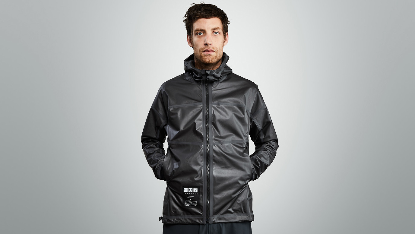
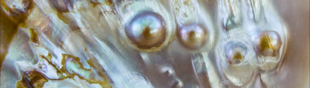
Courtesy: Vollebak
From an August 14, 2018 article by Jesus Diaz for Fast Company,
Graphene is the thinnest possible form of graphite, which you can find in your everyday pencil. It’s purely bi-dimensional, a single layer of carbon atoms that has unbelievable properties that have long threatened to revolutionize everything from aerospace engineering to medicine. …
Despite its immense promise, graphene still hasn’t found much use in consumer products, thanks to the fact that it’s hard to manipulate and manufacture in industrial quantities. The process of developing Vollebak’s jacket, according to the company’s cofounders, brothers Steve and Nick Tidball, took years of intensive research, during which the company worked with the same material scientists who built Michael Phelps’ 2008 Olympic Speedo swimsuit (which was famously banned for shattering records at the event).
…
The jacket is made out of a two-sided material, which the company invented during the extensive R&D process. The graphene side looks gunmetal gray, while the flipside appears matte black. To create it, the scientists turned raw graphite into something called graphene “nanoplatelets,” which are stacks of graphene that were then blended with polyurethane to create a membrane. That, in turn, is bonded to nylon to form the other side of the material, which Vollebak says alters the properties of the nylon itself. “Adding graphene to the nylon fundamentally changes its mechanical and chemical properties–a nylon fabric that couldn’t naturally conduct heat or energy, for instance, now can,” the company claims.
The company says that it’s reversible so you can enjoy graphene’s properties in different ways as the material interacts with either your skin or the world around you. “As physicists at the Max Planck Institute revealed, graphene challenges the fundamental laws of heat conduction, which means your jacket will not only conduct the heat from your body around itself to equalize your skin temperature and increase it, but the jacket can also theoretically store an unlimited amount of heat, which means it can work like a radiator,” Tidball explains.
He means it literally. You can leave the jacket out in the sun, or on another source of warmth, as it absorbs heat. Then, the company explains on its website, “If you then turn it inside out and wear the graphene next to your skin, it acts like a radiator, retaining its heat and spreading it around your body. The effect can be visibly demonstrated by placing your hand on the fabric, taking it away and then shooting the jacket with a thermal imaging camera. The heat of the handprint stays long after the hand has left.”
…
There’s a lot more to the article although it does feature some hype and I’m not sure I believe Diaz’s claim (August 14, 2018 article) that ‘graphene-based’ hair dye is perfectly safe ( Note: A link has been removed),
Graphene is the thinnest possible form of graphite, which you can find in your everyday pencil. It’s purely bi-dimensional, a single layer of carbon atoms that has unbelievable properties that will one day revolutionize everything from aerospace engineering to medicine. Its diverse uses are seemingly endless: It can stop a bullet if you add enough layers. It can change the color of your hair with no adverse effects. [emphasis mine] It can turn the walls of your home into a giant fire detector. “It’s so strong and so stretchy that the fibers of a spider web coated in graphene could catch a falling plane,” as Vollebak puts it in its marketing materials.
Not unless things have changed greatly since March 2018. My August 2, 2018 posting featured the graphene-based hair dye announcement from March 2018 and a cautionary note from Dr. Andrew Maynard (scroll down ab out 50% of the way for a longer excerpt of Maynard’s comments),
Northwestern University’s press release proudly announced, “Graphene finds new application as nontoxic, anti-static hair dye.” The announcement spawned headlines like “Enough with the toxic hair dyes. We could use graphene instead,” and “’Miracle material’ graphene used to create the ultimate hair dye.”
From these headlines, you might be forgiven for getting the idea that the safety of graphene-based hair dyes is a done deal. Yet having studied the potential health and environmental impacts of engineered nanomaterials for more years than I care to remember, I find such overly optimistic pronouncements worrying – especially when they’re not backed up by clear evidence.
…
These studies need to be approached with care, as the precise risks of graphene exposure will depend on how the material is used, how exposure occurs and how much of it is encountered. Yet there’s sufficient evidence to suggest that this substance should be used with caution – especially where there’s a high chance of exposure or that it could be released into the environment.
…
The full text of Dr. Maynard’s comments about graphene hair dyes and risk can be found here.
Bearing in mind that graphene-based hair dye is an entirely different class of product from the jacket, I wouldn’t necessarily dismiss risks; I would like to know what kind of risk assessment and safety testing has been done. Due to their understandable enthusiasm, the brothers Tidball have focused all their marketing on the benefits and the opportunity for the consumer to test their product (from graphene jacket product webpage),
While it’s completely invisible and only a single atom thick, graphene is the lightest, strongest, most conductive material ever discovered, and has the same potential to change life on Earth as stone, bronze and iron once did. But it remains difficult to work with, extremely expensive to produce at scale, and lives mostly in pioneering research labs. So following in the footsteps of the scientists who discovered it through their own highly speculative experiments, we’re releasing graphene-coated jackets into the world as experimental prototypes. Our aim is to open up our R&D and accelerate discovery by getting graphene out of the lab and into the field so that we can harness the collective power of early adopters as a test group. No-one yet knows the true limits of what graphene can do, so the first edition of the Graphene Jacket is fully reversible with one side coated in graphene and the other side not. If you’d like to take part in the next stage of this supermaterial’s history, the experiment is now open. You can now buy it, test it and tell us about it. [emphasis mine]
…
How maverick experiments won the Nobel Prize
While graphene’s existence was first theorised in the 1940s, it wasn’t until 2004 that two maverick scientists, Andre Geim and Konstantin Novoselov, were able to isolate and test it. Through highly speculative and unfunded experimentation known as their ‘Friday night experiments,’ they peeled layer after layer off a shaving of graphite using Scotch tape until they produced a sample of graphene just one atom thick. After similarly leftfield thinking won Geim the 2000 Ig Nobel prize for levitating frogs using magnets, the pair won the Nobel prize in 2010 for the isolation of graphene.
…
Should you be interested, in beta-testing the jacket, it will cost you $695 (presumably USD); order here. One last thing, Vollebak is based in the UK.
Graphene skinned plane
An August 14, 2018 news item (also published as an August 1, 2018 Haydale press release) by Sue Keighley on Azonano heralds a new technology for airplans,
Haydale, (AIM: HAYD), the global advanced materials group, notes the announcement made yesterday from the University of Central Lancashire (UCLAN) about the recent unveiling of the world’s first graphene skinned plane at the internationally renowned Farnborough air show.
The prepreg material, developed by Haydale, has potential value for fuselage and wing surfaces in larger scale aero and space applications especially for the rapidly expanding drone market and, in the longer term, the commercial aerospace sector. By incorporating functionalised nanoparticles into epoxy resins, the electrical conductivity of fibre-reinforced composites has been significantly improved for lightning-strike protection, thereby achieving substantial weight saving and removing some manufacturing complexities.
Before getting to the photo, here’s a definition for pre-preg from its Wikipedia entry (Note: Links have been removed),
Pre-preg is “pre-impregnated” composite fibers where a thermoset polymer matrix material, such as epoxy, or a thermoplastic resin is already present. The fibers often take the form of a weave and the matrix is used to bond them together and to other components during manufacture.
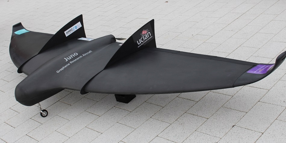
Haydale has supplied graphene enhanced prepreg material for Juno, a three-metre wide graphene-enhanced composite skinned aircraft, that was revealed as part of the ‘Futures Day’ at Farnborough Air Show 2018. [downloaded from https://www.azonano.com/news.aspx?newsID=36298]
A
July 31, 2018 University of Central Lancashire (UCLan) press release provides a tiny bit more (pun intended) detail,
The University of Central Lancashire (UCLan) has unveiled the world’s first graphene skinned plane at an internationally renowned air show.
Juno, a three-and-a-half-metre wide graphene skinned aircraft, was revealed on the North West Aerospace Alliance (NWAA) stand as part of the ‘Futures Day’ at Farnborough Air Show 2018.
The University’s aerospace engineering team has worked in partnership with the Sheffield Advanced Manufacturing Research Centre (AMRC), the University of Manchester’s National Graphene Institute (NGI), Haydale Graphene Industries (Haydale) and a range of other businesses to develop the unmanned aerial vehicle (UAV), which also includes graphene batteries and 3D printed parts.
Billy Beggs, UCLan’s Engineering Innovation Manager, said: “The industry reaction to Juno at Farnborough was superb with many positive comments about the work we’re doing. Having Juno at one the world’s biggest air shows demonstrates the great strides we’re making in leading a programme to accelerate the uptake of graphene and other nano-materials into industry.
“The programme supports the objectives of the UK Industrial Strategy and the University’s Engineering Innovation Centre (EIC) to increase industry relevant research and applications linked to key local specialisms. Given that Lancashire represents the fourth largest aerospace cluster in the world, there is perhaps no better place to be developing next generation technologies for the UK aerospace industry.”
Previous graphene developments at UCLan have included the world’s first flight of a graphene skinned wing and the launch of a specially designed graphene-enhanced capsule into near space using high altitude balloons.
UCLan engineering students have been involved in the hands-on project, helping build Juno on the Preston Campus.
Haydale supplied much of the material and all the graphene used in the aircraft. Ray Gibbs, Chief Executive Officer, said: “We are delighted to be part of the project team. Juno has highlighted the capability and benefit of using graphene to meet key issues faced by the market, such as reducing weight to increase range and payload, defeating lightning strike and protecting aircraft skins against ice build-up.”
David Bailey Chief Executive of the North West Aerospace Alliance added: “The North West aerospace cluster contributes over £7 billion to the UK economy, accounting for one quarter of the UK aerospace turnover. It is essential that the sector continues to develop next generation technologies so that it can help the UK retain its competitive advantage. It has been a pleasure to support the Engineering Innovation Centre team at the University in developing the world’s first full graphene skinned aircraft.”
The Juno project team represents the latest phase in a long-term strategic partnership between the University and a range of organisations. The partnership is expected to go from strength to strength following the opening of the £32m EIC facility in February 2019.
The next step is to fly Juno and conduct further tests over the next two months.
Next item, a new carbon material.
Schwarzite
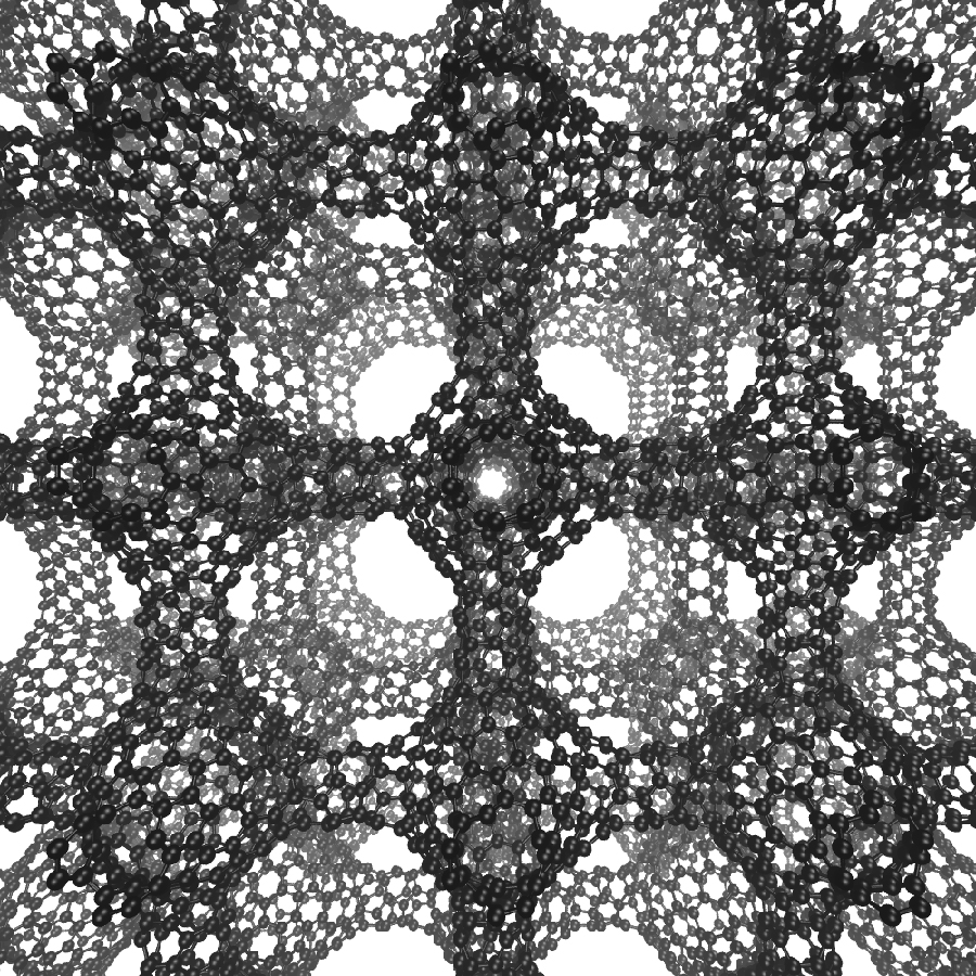
I love watching this gif of a schwarzite,
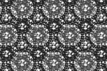
The three-dimensional cage structure of a schwarzite that was formed inside the pores of a zeolite. (Graphics by Yongjin Lee and Efrem Braun)
An August 13, 2018 news item on Nanowerk announces the new carbon structure,
The discovery of buckyballs [also known as fullerenes, C60, or buckminsterfullerenes] surprised and delighted chemists in the 1980s, nanotubes jazzed physicists in the 1990s, and graphene charged up materials scientists in the 2000s, but one nanoscale carbon structure – a negatively curved surface called a schwarzite – has eluded everyone. Until now.
University of California, Berkeley [UC Berkeley], chemists have proved that three carbon structures recently created by scientists in South Korea and Japan are in fact the long-sought schwarzites, which researchers predict will have unique electrical and storage properties like those now being discovered in buckminsterfullerenes (buckyballs or fullerenes for short), nanotubes and graphene.
An August 13, 2018 UC Berkeley news release by Robert Sanders, which originated the news item, describes how the Berkeley scientists and the members of their international collaboration from Germany, Switzerland, Russia, and Italy, have contributed to the current state of schwarzite research,
The new structures were built inside the pores of zeolites, crystalline forms of silicon dioxide – sand – more commonly used as water softeners in laundry detergents and to catalytically crack petroleum into gasoline. Called zeolite-templated carbons (ZTC), the structures were being investigated for possible interesting properties, though the creators were unaware of their identity as schwarzites, which theoretical chemists have worked on for decades.
Based on this theoretical work, chemists predict that schwarzites will have unique electronic, magnetic and optical properties that would make them useful as supercapacitors, battery electrodes and catalysts, and with large internal spaces ideal for gas storage and separation.
UC Berkeley postdoctoral fellow Efrem Braun and his colleagues identified these ZTC materials as schwarzites based of their negative curvature, and developed a way to predict which zeolites can be used to make schwarzites and which can’t.
“We now have the recipe for how to make these structures, which is important because, if we can make them, we can explore their behavior, which we are working hard to do now,” said Berend Smit, an adjunct professor of chemical and biomolecular engineering at UC Berkeley and an expert on porous materials such as zeolites and metal-organic frameworks.
Smit, the paper’s corresponding author, Braun and their colleagues in Switzerland, China, Germany, Italy and Russia will report their discovery this week in the journal Proceedings of the National Academy of Sciences. Smit is also a faculty scientist at Lawrence Berkeley National Laboratory.
Playing with carbon
Diamond and graphite are well-known three-dimensional crystalline arrangements of pure carbon, but carbon atoms can also form two-dimensional “crystals” — hexagonal arrangements patterned like chicken wire. Graphene is one such arrangement: a flat sheet of carbon atoms that is not only the strongest material on Earth, but also has a high electrical conductivity that makes it a promising component of electronic devices.

The cage structure of a schwarzite that was formed inside the pores of a zeolite. The zeolite is subsequently dissolved to release the new material. (Graphics by Yongjin Lee and Efrem Braun)
Graphene sheets can be wadded up to form soccer ball-shaped fullerenes – spherical carbon cages that can store molecules and are being used today to deliver drugs and genes into the body. Rolling graphene into a cylinder yields fullerenes called nanotubes, which are being explored today as highly conductive wires in electronics and storage vessels for gases like hydrogen and carbon dioxide. All of these are submicroscopic, 10,000 times smaller than the width of a human hair.
To date, however, only positively curved fullerenes and graphene, which has zero curvature, have been synthesized, feats rewarded by Nobel Prizes in 1996 and 2010, respectively.
In the 1880s, German physicist Hermann Schwarz investigated negatively curved structures that resemble soap-bubble surfaces, and when theoretical work on carbon cage molecules ramped up in the 1990s, Schwarz’s name became attached to the hypothetical negatively curved carbon sheets.
“The experimental validation of schwarzites thus completes the triumvirate of possible curvatures to graphene; positively curved, flat, and now negatively curved,” Braun added.
Minimize me
Like soap bubbles on wire frames, schwarzites are topologically minimal surfaces. When made inside a zeolite, a vapor of carbon-containing molecules is injected, allowing the carbon to assemble into a two-dimensional graphene-like sheet lining the walls of the pores in the zeolite. The surface is stretched tautly to minimize its area, which makes all the surfaces curve negatively, like a saddle. The zeolite is then dissolved, leaving behind the schwarzite.

A computer-rendered negatively curved soap bubble that exhibits the geometry of a carbon schwarzite. (Felix Knöppel image)
“These negatively-curved carbons have been very hard to synthesize on their own, but it turns out that you can grow the carbon film catalytically at the surface of a zeolite,” Braun said. “But the schwarzites synthesized to date have been made by choosing zeolite templates through trial and error. We provide very simple instructions you can follow to rationally make schwarzites and we show that, by choosing the right zeolite, you can tune schwarzites to optimize the properties you want.”
Researchers should be able to pack unusually large amounts of electrical charge into schwarzites, which would make them better capacitors than conventional ones used today in electronics. Their large interior volume would also allow storage of atoms and molecules, which is also being explored with fullerenes and nanotubes. And their large surface area, equivalent to the surface areas of the zeolites they’re grown in, could make them as versatile as zeolites for catalyzing reactions in the petroleum and natural gas industries.
Braun modeled ZTC structures computationally using the known structures of zeolites, and worked with topological mathematician Senja Barthel of the École Polytechnique Fédérale de Lausanne in Sion, Switzerland, to determine which of the minimal surfaces the structures resembled.
The team determined that, of the approximately 200 zeolites created to date, only 15 can be used as a template to make schwarzites, and only three of them have been used to date to produce schwarzite ZTCs. Over a million zeolite structures have been predicted, however, so there could be many more possible schwarzite carbon structures made using the zeolite-templating method.
Other co-authors of the paper are Yongjin Lee, Seyed Mohamad Moosavi and Barthel of the École Polytechnique Fédérale de Lausanne, Rocio Mercado of UC Berkeley, Igor Baburin of the Technische Universität Dresden in Germany and Davide Proserpio of the Università degli Studi di Milano in Italy and Samara State Technical University in Russia.
Here’s a link to and a citation for the paper,
Generating carbon schwarzites via zeolite-templating by Efrem Braun, Yongjin Lee, Seyed Mohamad Moosavi, Senja Barthel, Rocio Mercado, Igor A. Baburin, Davide M. Proserpio, and Berend Smit. PNAS August 14, 2018. 201805062; published ahead of print August 14, 2018. https://doi.org/10.1073/pnas.1805062115
This paper appears to be open access.