Tag Archives: University of Illinois at Urbana-Champaign

What do nanocrystals have in common with the earth’s crust?

The deformation properties of nanocrystals resemble those in the earth’s crust according to a Nov. 17, 2015 news item on Nanowerk,

Apparently, size doesn’t always matter. An extensive study by an interdisciplinary research group suggests that the deformation properties of nanocrystals are not much different from those of the Earth’s crust.

“When solid materials such as nanocrystals, bulk metallic glasses, rocks, or granular materials are slowly deformed by compression or shear, they slip intermittently with slip-avalanches similar to earthquakes,” explained Karin Dahmen, a professor of physics at the University of Illinois at Urbana-Champaign. “Typically these systems are studied separately. But we found that the scaling behavior of their slip statistics agree across a surprisingly wide range of different length scales and material structures.”

There’s an illustration accompanying the research,

Courtesy of the University of Illinois

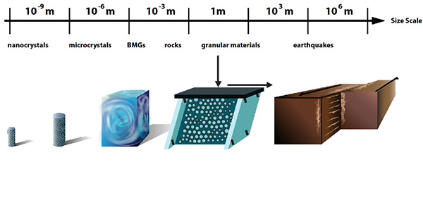
Caption: When solid materials such as nanocrystals, bulk metallic glasses, rocks, or granular materials are slowly deformed by compression or shear, they slip intermittently with slip-avalanches similar to earthquakes. Credit: University of Illinois

A Nov. 17, 2015 University of Illinois news release (also on EurekAlert) by Rick Kubetz, which originated the news item, provides more detail,

“Identifying agreement in aspects of the slip statistics is important, because it enables us to transfer results from one scale to another, from one material to another, from one stress to another, or from one strain rate to another,” stated Shivesh Pathak, a physics undergraduate at Illinois, and a co-author of the paper, “Universal Quake Statistics: From Compressed Nanocrystals to Earthquakes,” appearing in Scientific Reports. “The study shows how to identify and explain commonalities in the deformation mechanisms of different materials on different scales.

“The results provide new tools and methods to use the slip statistics to predict future materials deformation,” added Michael LeBlanc, a physics graduate student and co-author of the paper. “They also clarify which system parameters significantly affect the deformation behavior on long length scales. We expect the results to be useful for applications in materials testing, failure prediction, and hazard prevention.”

Researchers representing a broad a range of disciplines–including physics, geosciences, mechanical engineering, chemical engineering, and materials science–from the United States, Germany, and the Netherlands contributed to the study, comparing five different experimental systems, on several different scales, with model predictions.

As a solid is sheared, each weak spot is stuck until the local shear stress exceeds a random failure threshold. It then slips by a random amount until it re-sticks. The released stress is redistributed to all other weak spots. Thus, a slipping weak spot can trigger other spots to fail in a slip avalanche.

Using tools from the theory of phase transitions, such as the renormalization group, one can show that the slip statistics of the model do not depend on the details of the system.

“Although these systems span 13 decades in length scale, they all show the same scaling behavior for their slip size distributions and other statistical properties,” stated Pathak. “Their size distributions follow the same simple (power law) function, multiplied with the same exponential cutoff.”

The cutoff, which is the largest slip or earthquake size, grows with applied force for materials spanning length scales from nanometers to kilometers. The dependence of the size of the largest slip or quake on stress reflects “tuned critical” behavior, rather than so-called self-organized criticality, which would imply stress-independence.

“The agreement of the scaling properties of the slip statistics across scales does not imply the predictability of individual slips or earthquakes,” LeBlanc said. “Rather, it implies that we can predict the scaling behavior of average properties of the slip statistics and the probability of slips of a certain size, including their dependence on stress and strain-rate.”

Here’s a link to and a citation for the paper,

Universal Quake Statistics: From Compressed Nanocrystals to Earthquakes by Jonathan T. Uhl, Shivesh Pathak, Danijel Schorlemmer, Xin Liu, Ryan Swindeman, Braden A. W. Brinkman, Michael LeBlanc, Georgios Tsekenis, Nir Friedman, Robert Behringer, Dmitry Denisov, Peter Schall, Xiaojun Gu, Wendelin J. Wright, Todd Hufnagel, Andrew Jennings, Julia R. Greer, P. K. Liaw, Thorsten Becker, Georg Dresen, & Karin A. Dahmen.  Scientific Reports 5, Article number: 16493 (2015)  doi:10.1038/srep16493 Published online: 17 November 2015

This is an open access paper.

One final comment, this story reminds me of a few other pieces of research featured here, which focus on repeating patterns in nature. The research was mentioned in an Aug. 27, 2015 posting about white dwarf stars and heartbeats and in an April 14, 2015 posting about gold nanoparticles and their resemblance to the Milky Way. You can also find more in the Wikipedia entry titled ‘Patterns in nature‘.

Nanopores and a new technique for desalination

There’s been more than one piece here about water desalination and purification and/or remediation efforts and at least one of them claims to have successfully overcome issues such as reverse osmosis energy needs which are hampering adoption of various technologies. Now, researchers at the University of Illinois at Champaign Urbana have developed another new technique for desalinating water while reverse osmosis issues according to a Nov. 11, 2015 news item on Nanowerk (Note: A link has been removed) ,

University of Illinois engineers have found an energy-efficient material for removing salt from seawater that could provide a rebuttal to poet Samuel Taylor Coleridge’s lament, “Water, water, every where, nor any drop to drink.”

The material, a nanometer-thick sheet of molybdenum disulfide (MoS2) riddled with tiny holes called nanopores, is specially designed to let high volumes of water through but keep salt and other contaminates out, a process called desalination. In a study published in the journal Nature Communications (“Water desalination with a single-layer MoS2 nanopore”), the Illinois team modeled various thin-film membranes and found that MoS2 showed the greatest efficiency, filtering through up to 70 percent more water than graphene membranes. [emphasis mine]

I’ll get to the professor’s comments about graphene membranes in a minute. Meanwhile, a Nov. 11, 2015 University of Illinois news release (also on EurekAlert), which originated the news item, provides more information about the research,

“Even though we have a lot of water on this planet, there is very little that is drinkable,” said study leader Narayana Aluru, a U. of I. professor of mechanical science and engineering. “If we could find a low-cost, efficient way to purify sea water, we would be making good strides in solving the water crisis.

“Finding materials for efficient desalination has been a big issue, and I think this work lays the foundation for next-generation materials. These materials are efficient in terms of energy usage and fouling, which are issues that have plagued desalination technology for a long time,” said Aluru, who also is affiliated with the Beckman Institute for Advanced Science and Technology at the U. of I.

Most available desalination technologies rely on a process called reverse osmosis to push seawater through a thin plastic membrane to make fresh water. The membrane has holes in it small enough to not let salt or dirt through, but large enough to let water through. They are very good at filtering out salt, but yield only a trickle of fresh water. Although thin to the eye, these membranes are still relatively thick for filtering on the molecular level, so a lot of pressure has to be applied to push the water through.

“Reverse osmosis is a very expensive process,” Aluru said. “It’s very energy intensive. A lot of power is required to do this process, and it’s not very efficient. In addition, the membranes fail because of clogging. So we’d like to make it cheaper and make the membranes more efficient so they don’t fail as often. We also don’t want to have to use a lot of pressure to get a high flow rate of water.”

One way to dramatically increase the water flow is to make the membrane thinner, since the required force is proportional to the membrane thickness. Researchers have been looking at nanometer-thin membranes such as graphene. However, graphene presents its own challenges in the way it interacts with water.

Aluru’s group has previously studied MoS2 nanopores as a platform for DNA sequencing and decided to explore its properties for water desalination. Using the Blue Waters supercomputer at the National Center for Supercomputing Applications at the U. of I., they found that a single-layer sheet of MoS2 outperformed its competitors thanks to a combination of thinness, pore geometry and chemical properties.

A MoS2 molecule has one molybdenum atom sandwiched between two sulfur atoms. A sheet of MoS2, then, has sulfur coating either side with the molybdenum in the center. The researchers found that creating a pore in the sheet that left an exposed ring of molybdenum around the center of the pore created a nozzle-like shape that drew water through the pore.

“MoS2 has inherent advantages in that the molybdenum in the center attracts water, then the sulfur on the other side pushes it away, so we have much higher rate of water going through the pore,” said graduate student Mohammad Heiranian, the first author of the study. “It’s inherent in the chemistry of MoS2 and the geometry of the pore, so we don’t have to functionalize the pore, which is a very complex process with graphene.”

In addition to the chemical properties, the single-layer sheets of MoS2 have the advantages of thinness, requiring much less energy, which in turn dramatically reduces operating costs. MoS2 also is a robust material, so even such a thin sheet is able to withstand the necessary pressures and water volumes.

The Illinois researchers are establishing collaborations to experimentally test MoS2 for water desalination and to test its rate of fouling, or clogging of the pores, a major problem for plastic membranes. MoS2 is a relatively new material, but the researchers believe that manufacturing techniques will improve as its high performance becomes more sought-after for various applications.

“Nanotechnology could play a great role in reducing the cost of desalination plants and making them energy efficient,” said Amir Barati Farimani, who worked on the study as a graduate student at Illinois and is now a postdoctoral fellow at Stanford University. “I’m in California now, and there’s a lot of talk about the drought and how to tackle it. I’m very hopeful that this work can help the designers of desalination plants. This type of thin membrane can increase return on investment because they are much more energy efficient.”

Here’s a link to and a citation for the paper,

Water desalination with a single-layer MoS2 nanopore by Mohammad Heiranian, Amir Barati Farimani, & Narayana R. Aluru. Nature Communications 6, Article number: 8616 doi:10.1038/ncomms9616 Published 14 October 2015

Graphene membranes

In a July 13, 2015 essay on Nanotechnology Now, Tim Harper provides an overview of the research into using graphene for water desalination and purification/remediation about which he is quite hopeful. There is no mention of an issue with interactions between water and graphene. It should be noted that Tim Harper is the Chief Executive Officer of G20, a company which produces a graphene-based solution (graphene oxide sheets), which can desalinate water and can purify/remediate it. Tim is a scientist and while you might have some hesitation given his fiscal interests, his essay is worthwhile reading as he supplies context and explanations of the science.

On the verge of controlling neurons by wireless?

Scientists have controlled a mouse’s neurons with a wireless device (and unleashed some paranoid fantasies? well, mine if no one else’s) according to a July 16, 2015 news item on Nanowerk (Note: A link has been removed),

A study showed that scientists can wirelessly determine the path a mouse walks with a press of a button. Researchers at the Washington University School of Medicine, St. Louis, and University of Illinois, Urbana-Champaign, created a remote controlled, next-generation tissue implant that allows neuroscientists to inject drugs and shine lights on neurons deep inside the brains of mice. The revolutionary device is described online in the journal Cell (“Wireless Optofluidic Systems for Programmable In Vivo Pharmacology and Optogenetics”). Its development was partially funded by the [US] National Institutes of Health [NIH].

The researchers have made an image/illustration of the probe available,

Mind Bending Probe Scientists used soft materials to create a brain implant a tenth the width of a human hair that can wirelessly control neurons with lights and drugs. Courtesy of Jeong lab, University of Colorado Boulder.

A July 16, 2015 US NIH National Institute of Neurological Disorders and Stroke news release, which originated the news item, describes the study and notes that instructions for building the implant are included in the published study,

“It unplugs a world of possibilities for scientists to learn how brain circuits work in a more natural setting.” said Michael R. Bruchas, Ph.D., associate professor of anesthesiology and neurobiology at Washington University School of Medicine and a senior author of the study.

The Bruchas lab studies circuits that control a variety of disorders including stress, depression, addiction, and pain. Typically, scientists who study these circuits have to choose between injecting drugs through bulky metal tubes and delivering lights through fiber optic cables. Both options require surgery that can damage parts of the brain and introduce experimental conditions that hinder animals’ natural movements.

To address these issues, Jae-Woong Jeong, Ph.D., a bioengineer formerly at the University of Illinois at Urbana-Champaign, worked with Jordan G. McCall, Ph.D., a graduate student in the Bruchas lab, to construct a remote controlled, optofluidic implant. The device is made out of soft materials that are a tenth the diameter of a human hair and can simultaneously deliver drugs and lights.

“We used powerful nano-manufacturing strategies to fabricate an implant that lets us penetrate deep inside the brain with minimal damage,” said John A. Rogers, Ph.D., professor of materials science and engineering, University of Illinois at Urbana-Champaign and a senior author. “Ultra-miniaturized devices like this have tremendous potential for science and medicine.”

With a thickness of 80 micrometers and a width of 500 micrometers, the optofluidic implant is thinner than the metal tubes, or cannulas, scientists typically use to inject drugs. When the scientists compared the implant with a typical cannula they found that the implant damaged and displaced much less brain tissue.

The scientists tested the device’s drug delivery potential by surgically placing it into the brains of mice. In some experiments, they showed that they could precisely map circuits by using the implant to inject viruses that label cells with genetic dyes. In other experiments, they made mice walk in circles by injecting a drug that mimics morphine into the ventral tegmental area (VTA), a region that controls motivation and addiction.

The researchers also tested the device’s combined light and drug delivery potential when they made mice that have light-sensitive VTA neurons stay on one side of a cage by commanding the implant to shine laser pulses on the cells. The mice lost the preference when the scientists directed the device to simultaneously inject a drug that blocks neuronal communication. In all of the experiments, the mice were about three feet away from the command antenna.

“This is the kind of revolutionary tool development that neuroscientists need to map out brain circuit activity,” said James Gnadt, Ph.D., program director at the NIH’s National Institute of Neurological Disorders and Stroke (NINDS).  “It’s in line with the goals of the NIH’s BRAIN Initiative.”

The researchers fabricated the implant using semi-conductor computer chip manufacturing techniques. It has room for up to four drugs and has four microscale inorganic light-emitting diodes. They installed an expandable material at the bottom of the drug reservoirs to control delivery. When the temperature on an electric heater beneath the reservoir rose then the bottom rapidly expanded and pushed the drug out into the brain.

“We tried at least 30 different prototypes before one finally worked,” said Dr. McCall.

“This was truly an interdisciplinary effort,” said Dr. Jeong, who is now an assistant professor of electrical, computer, and energy engineering at University of Colorado Boulder. “We tried to engineer the implant to meet some of neurosciences greatest unmet needs.”

In the study, the scientists provide detailed instructions for manufacturing the implant.

“A tool is only good if it’s used,” said Dr. Bruchas. “We believe an open, crowdsourcing approach to neuroscience is a great way to understand normal and healthy brain circuitry.”

Here’s a link to and a citation for the paper,

Wireless Optofluidic Systems for Programmable In Vivo Pharmacology and Optogenetics by Jae-Woong Jeong, Jordan G. McCall, Gunchul Shin, Yihui Zhang, Ream Al-Hasani, Minku Kim, Shuo Li, Joo Yong Sim, Kyung-In Jang, Yan Shi, Daniel Y. Hong, Yuhao Liu, Gavin P. Schmitz, Li Xia, Zhubin He, Paul Gamble, Wilson Z. Ray, Yonggang Huang, Michael R. Bruchas, and John A. Rogers.  Cell, July 16, 2015. DOI: 10.1016/j.cell.2015.06.058

This paper is behind a paywall.

I last wrote about wireless activation of neurons in a May 28, 2014 posting which featured research at the University of Massachusetts Medical School.

Silk inks containing enzymes, antibiotics, antibodies, nanoparticles, and growth factors

There’s an almost euphoric tone to a June 16, 2015 Tufts University news release (also on EurekAlert) about research which has resulted in the ability to print silk-based inks,

Silk inks containing enzymes, antibiotics, antibodies, nanoparticles and growth factors could turn inkjet printing into a new, more effective tool for therapeutics, regenerative medicine and biosensing, according to new research led by Tufts University  biomedical engineers and published June 16 [2015] in the journal Advanced Materials online in advance of print.

Until now, heat used in the inkjet printing process made using silk a challenge (as it does for cellulose nanomaterials used in 3D printers, noted in my June 17, 2015 posting), from the Tufts news release,

Inkjet printing is one of the most immediate and accessible forms of printing technology currently available, according to the researchers, and ink-jet printing of biomolecules has been previously proposed by scientists. However, the heat-sensitive nature of these unstable compounds means printed materials rapidly lose functionality, limiting their use.

Enter purified silk protein, or fibroin, which offers intrinsic strength and protective properties that make it well-suited for a range of biomedical and optoelectronic applications. This natural polymer is an ideal “cocoon” that can stabilize compounds such as enzymes, antibodies and growth factors while lending itself to many different mechanically robust formats, said Fiorenzo Omenetto, Ph.D., senior author on the paper and associate dean for research and Frank C. Doble Professor of Engineering at Tufts School of Engineering.

“We thought that if we were able to develop an inkjet-printable silk solution, we would have a universal building block to generate multiple functional printed formats that could lead to a wide variety of applications in which inks remain active over time,” he said.

By using this simple approach and starting with the same base material, the research team created and tested a “custom library” of inkjet-printable, functional silk inks doped with a variety of components:

  • Bacterial-sensing polydiacetylenes (PDAs) printed on surgical gloves; the word “contaminated” printed on the glove changed from blue to red after exposure to E. coli
  • Proteins that stimulate bone growth (BMP-2) printed on a plastic dish to test topographical control of directed tissue growth
  • Sodium ampicillin printed on a bacterial culture to test the effectiveness of a topographical distribution of the antibiotic
  • Gold nanoparticles printed on paper, for possible application in photonics and biology (e.g., color engineering, surface plasmon resonance based sensing and bio-imaging)
  • Enzymes printed on paper to test the ability of the ink to entrain small functional biomolecules

The researchers, who included collaborators from the University of Illinois at Urbana-Champaign, foresee wide potential for future investigation and application of this technology.

For example, Omenetto envisions more work on the bio-sensing gloves, which he says could selectively react to different pathological agents. The ability to print antibiotics in topographical patterns could address the need for “smart” bandages, where therapeutics are incorporated and delivered to match a complex injury.

The published research was restricted to one ink cartridge, but the scientists believe it could extend to multi-cartridge printing combining complex functions.

Omenetto and Kaplan are pioneers in the use of silk as an alternative to plastics. Omenetto’s 2011 TED Talk called silk a “new old material” that could have a profound impact in many technical fields.

Here’s a link to and citation for the paper,

Inkjet Printing of Regenerated Silk Fibroin: From Printable Forms to Printable Functions by Hu Tao, Benedetto marelli, Miaomiao Yang, Bo An, Serdar Onses, John A. Rogers, David L. Kaplan, & Fiorenzo G. Omenetto. Advanced Materials DOI: 10.1002/adma.201501425 First published: 16 June 2015

This article is behind a paywall.

A divisive scientific/philosophical debate that changed everything: Einstein vs. Bergson on the nature of time

A feud between a scientist and a philosopher—this seems like the setup for a joke but it’s not. According to a May 26, 2015 news item on phys.org, the book ‘The Physicist and the Philosopher: Einstein, Bergson, and the Debate That Changed Our Understanding of Time‘ chronicles a seminal debate and conflict that reverberates to this day,

Two of the 20th century’s greatest minds, one of them physicist Albert Einstein, came to intellectual blows one day in Paris in 1922. Their dispute, before a learned audience, was about the nature of time – mostly in connection with Einstein’s most famous work, the theory of relativity, which marks its centennial this year.

One immediate result of the controversy: There would be no mention of relativity in Einstein’s Nobel Prize, awarded a few months later.

One long-term result: a split between science and the humanities that continues to this day.

A May 26, 2015 University of Illinois at Urbana-Champaign news release, which originated the news item, provides some insight into a fascinating story,

The philosopher in the title, and Einstein’s adversary that day, was Henri Bergson, a French philosopher who was much more famous at the time than the German-born Einstein. Presidents and prime ministers carefully read Bergson’s work, and his public lectures often were filled to capacity. He was perhaps the pre-eminent public intellectual of his time, Canales [said.

Bergson did not challenge Einstein’s scientific claims about relativity, including the then-startling claim of time dilation, in which time slows down for objects traveling at higher speeds, Canales said.

What he challenged instead was Einstein’s interpretation of those claims, saying it went beyond science and was “a metaphysics grafted upon science.” He said that Einstein’s theory did not consider time as it was lived in human experience, the aspects of time that could not be captured by clocks or formulas.

Einstein quickly dismissed the philosopher’s criticism. To an audience that day of mostly philosophers, he made the incendiary statement that “the time of the philosophers does not exist.”

In the aftermath, Bergson published a book in which he thoroughly laid out his criticism of Einstein’s relativity and his theory of time. Both men and their supporters also spread their views through publications and letters, some of which employed “highly effective backbiting,” Canales said.

Bergson and Einstein also seemed to be on opposite ends of almost every pertinent issue of the time, from war and peace to race and faith, she said. “They seemed to take opposite stances in everything.”

Einstein supporters claimed that Bergson, though a gifted mathematician, did not completely understand Einstein’s theory. Bergson thought his theory of time was misunderstood by Einstein.

Bergson’s influence has been most prominent in novels and film, in their use of narrative twists and breaks and in time-shifting between past and future, Canales said. He also has had support among scientists, among them leading physicists who had helped develop relativity, as well as experts on quantum mechanics.

It was Einstein’s ideas that gained prominence, however, in part because later research only reinforced the science of relativity, but also because Bergson was effectively discredited by scientists, Canales said. Outside of philosophy, Bergson has been largely forgotten and is rarely even mentioned in Einstein biographies.

Canales said her book tells a “backstory of the rise of science” in the 20th century. It’s a story of “misunderstanding and mistrust,” she said.

“I took a pessimistic view of human nature and of our capacity to understand each other, and I think that view actually illuminates why so many humanists cannot talk to scientists, and scientists cannot talk to humanists.”

Canales said she sought to give an even-handed treatment to the two men and their views. In the process, however, she also sought to rehabilitate Bergson.

Just as Bergson was painted by some as anti-science, Canales said she knows she takes a similar risk in trying to give him his due in the dispute with Einstein, though it is not her intent. Being against science in the modern world, “makes no sense,” she said. “Clearly we should be for science.”

But we also need to think about science critically, Canales said. “We’re not taught to see science as it really is, as it really is practiced, as it really is done.” She said she hopes her book might help scientists and others understand the place of science “in more realistic terms.”

Canales’ book was published by Princeton University Press May 26, 2015. ‘The Physicist and the Philosopher: Einstein, Bergson, and the Debate That Changed Our Understanding of Time’ can be purchased here.

I expect anyone who reads this blog is likely to be familiar with Einstein but perhaps less so with Bergson. Here’s more about Bergson from his Wikipedia entry (Note: Links have been removed),

Henri-Louis Bergson (French: [bɛʁksɔn]; 18 October 1859 – 4 January 1941) was a major French philosopher, influential especially in the first half of the 20th century. Bergson convinced many thinkers that the processes of immediate experience and intuition are more significant than abstract rationalism and science for understanding reality. Bergson had a long affair with musicologist Janet Levy which led to her article “A Source of Musical Wit and Humor.” This was a well-regarded article used by many later writers.

He was awarded the 1927 Nobel Prize in Literature “in recognition of his rich and vitalizing ideas and the brilliant skill with which they have been presented”.[2] In 1930 France awarded him its highest honour, the Grand-Croix de la Legion d’honneur.

Twinkle, Twinkle Little Star (song) could lead to better data storage

A March 16, 2015 news item on Nanowerk features research from the University of Illinois and the song ‘Twinkle, Twinkle Little Star’,

Researchers from the University of Illinois at Urbana-Champaign have demonstrated the first-ever recording of optically encoded audio onto a non-magnetic plasmonic nanostructure, opening the door to multiple uses in informational processing and archival storage.

“The chip’s dimensions are roughly equivalent to the thickness of human hair,” explained Kimani Toussaint, an associate professor of mechanical science and engineering, who led the research.

Specifically, the photographic film property exhibited by an array of novel gold, pillar-supported bowtie nanoantennas (pBNAs)–previously discovered by Toussaint’s group–was exploited to store sound and audio files. Compared with the conventional magnetic film for analog data storage, the storage capacity of pBNAs is around 5,600 times larger, indicating a vast array of potential storage uses.

The researchers have provide a visual image illustrating their work,

Nano piano concept: Arrays of gold, pillar-supported bowtie nanoantennas (bottom left) can be used to record distinct musical notes, as shown in the experimentally obtained dark-field microscopy images (bottom right). These particular notes were used to compose 'Twinkle, Twinkle, Little Star.'  Courtesy of University of Illinois at Urbana-Champaign

Nano piano concept: Arrays of gold, pillar-supported bowtie nanoantennas (bottom left) can be used to record distinct musical notes, as shown in the experimentally obtained dark-field microscopy images (bottom right). These particular notes were used to compose ‘Twinkle, Twinkle, Little Star.’ Courtesy of University of Illinois at Urbana-Champaign

A March 16, 2015 University of Illinois at Urbana-Champaign news release (also on EurekAlert), which originated the news item, describes the research in more detail (Note: Links have been removed),

To demonstrate its abilities to store sound and audio files, the researchers created a musical keyboard or “nano piano,” using the available notes to play the short song, “Twinkle, Twinkle, Little Star.”

“Data storage is one interesting area to think about,” Toussaint said. “For example, one can consider applying this type of nanotechnology to enhancing the niche, but still important, analog technology used in the area of archival storage such as using microfiche. In addition, our work holds potential for on-chip, plasmonic-based information processing.”

The researchers demonstrated that the pBNAs could be used to store sound information either as a temporally varying intensity waveform or a frequency varying intensity waveform. Eight basic musical notes, including middle C, D, and E, were stored on a pBNA chip and then retrieved and played back in a desired order to make a tune.

“A characteristic property of plasmonics is the spectrum,” said Hao Chen, a former postdoctoral researcher in Toussaint’s PROBE laboratory and the first author of the paper, “Plasmon-Assisted Audio Recording,” appearing in the Nature Publishing Group’s Scientific Reports. “Originating from a plasmon-induced thermal effect, well-controlled nanoscale morphological changes allow as much as a 100-nm spectral shift from the nanoantennas. By employing this spectral degree-of-freedom as an amplitude coordinate, the storage capacity can be improved. Moreover, although our audio recording focused on analog data storage, in principle it is still possible to transform to digital data storage by having each bowtie serve as a unit bit 1 or 0. By modifying the size of the bowtie, it’s feasible to further improve the storage capacity.”

The team previously demonstrated that pBNAs experience reduced thermal conduction in comparison to standard bowtie nanoantennas and can easily get hot when irradiated by low-powered laser light. Each bowtie antenna is approximately 250 nm across in dimensions, with each supported on 500-nm tall silicon dioxide posts. A consequence of this is that optical illumination results in subtle melting of the gold, and thus a change in the overall optical response. This shows up as a difference in contrast under white-light illumination.

“Our approach is analogous to the method of ‘optical sound,’ which was developed circa 1920s as part of the effort to make ‘talking’ motion pictures,” the team said in its paper. “Although there were variations of this process, they all shared the same basic principle. An audio pickup, e.g., a microphone, electrically modulates a lamp source. Variations in the intensity of the light source is encoded on semi-transparent photographic film (e.g., as variation in area) as the film is spatially translated. Decoding this information is achieved by illuminating the film with the same light source and picking up the changes in the light transmission on an optical detector, which in turn may be connected to speakers. In the work that we present here, the pBNAs serve the role of the photographic film which we can encode with audio information via direct laser writing in an optical microscope.”

In their approach, the researchers record audio signals by using a microscope to scan a sound-modulated laser beam directly on their nanostructures. Retrieval and subsequent playback is achieved by using the same microscope to image the recorded waveform onto a digital camera, whereby simple signal processing can be performed.

Here’s a link to and a citation for the paper,

Plasmon-Assisted Audio Recording by Hao Chen, Abdul M. Bhuiya, Qing Ding, & Kimani C. Toussaint, Jr. Scientific Reports 5, Article number: 9125 doi:10.1038/srep09125 Published 16 March 2015

This is an open access paper and here is a sample recording courtesy of the researchers and the University of Illinois at Urbana-Champaign,

Crumpling graphene to create a 3D structure and reflattening it afterwards

The reseaarchers at the University of Illinois College of Engineering are quite excited about a new technique for crumpling graphene as a Feb. 17, 2015 news item on ScienceDaily reports,

Researchers at the University of Illinois at Urbana-Champaign have developed a unique single-step process to achieve three-dimensional (3D) texturing of graphene and graphite. Using a commercially available thermally activated shape-memory polymer substrate, this 3D texturing, or “crumpling,” allows for increased surface area and opens the doors to expanded capabilities for electronics and biomaterials.

“Fundamentally, intrinsic strains on crumpled graphene could allow modulation of electrical and optical properties of graphene,” explained SungWoo Nam, an assistant professor of mechanical science and engineering at Illinois. “We believe that the crumpled graphene surfaces can be used as higher surface area electrodes for battery and supercapacitor applications. As a coating layer, 3D textured/crumpled nano-topographies could allow omniphobic/anti-bacterial surfaces for advanced coating applications.”

A Feb. 16, 2015 University of Illinois College of Engineering news release (also on EurekAlert), which originated the news item, describes the nature of graphene and what makes this technique so exciting,

Graphene—a single atomic layer of sp2-bonded carbon atoms—has been a material of intensive research and interest over recent years.  A combination of exceptional mechanical properties, high carrier mobility, thermal conductivity, and chemical inertness, make graphene a prime candidate material for next generation optoelectronic, electromechanical, and biomedical applications.

“In this study, we developed a novel method for controlled crumpling of graphene and graphite via heat-induced contractile deformation of the underlying substrate,” explained Michael Cai Wang, a graduate student and first author of the paper, “Heterogeneous, Three-Dimensional Texturing of Graphene,” which appeared in the journal Nano Letters. ”While graphene intrinsically exhibits tiny ripples in ambient conditions, we created large and tunable crumpled textures in a tailored and scalable fashion.”

“As a simpler, more scalable, and spatially selective method, this texturing of graphene and graphite exploits the thermally induced transformation of shape-memory thermoplastics, which has been previously applied to microfluidic device fabrication, metallic  film patterning, nanowire assembly, and robotic self-assembly applications,” added Nam, whose group has filed a patent for their novel strategy. “The thermoplastic nature of the polymeric substrate also allows for the crumpled graphene morphology to be arbitrarily re-flattened at the same elevated temperature for the crumpling process.”

“Due to the extremely low cost and ease of processing of our approach, we believe that this will be a new way to manufacture nanoscale topographies for graphene and many other 2D and thin-film materials.”

The researchers are also investigating the textured graphene surfaces for 3D sensor applications.

“Enhanced surface area will allow even more sensitive and intimate interactions with biological systems, leading to high sensitivity devices,” Nam said.

The funding agencies for this project were unexpectedly interesting (to me), from the news release,

Funding for this research was provided through the Air Force Office for Scientific Research, American Chemical Society and Brain Research Foundation. [emphasis mine] In addition to Wang, co-authors from Nam’s research group at Illinois include SungGyu Chun, Ryan Han, Ali Ashraf, and Pilgyu Kang.

Here’s a link to and a citation for the paper,

Heterogeneous, Three-Dimensional Texturing of Graphene by Michael Cai Wang, SungGyu Chun, Ryan Steven Han, Ali Ashraf, Pilgyu Kang, and SungWoo Nam. Nano Lett., Article ASAP
DOI: 10.1021/nl504612y Publication Date (Web): February 10, 2015

Copyright © 2015 American Chemical Society

This paper is behind a paywall.

Dexter Johnson has written a Feb. 20, 2015 post highlighting this work on his Nanoclast blog (on the Institute of Electrical and Electronics Engineers [IEEE] website).

Self-organizing nanotubes and nonequilibrium systems provide insights into evolution and artificial life

If you’re interested in the second law of thermodynamics, this Feb. 10, 2015 news item on ScienceDaily provides some insight into the second law, self-organized systems, and evolution,

The second law of thermodynamics tells us that all systems evolve toward a state of maximum entropy, wherein all energy is dissipated as heat, and no available energy remains to do work. Since the mid-20th century, research has pointed to an extension of the second law for nonequilibrium systems: the Maximum Entropy Production Principle (MEPP) states that a system away from equilibrium evolves in such a way as to maximize entropy production, given present constraints.

Now, physicists Alexey Bezryadin, Alfred Hubler, and Andrey Belkin from the University of Illinois at Urbana-Champaign, have demonstrated the emergence of self-organized structures that drive the evolution of a non-equilibrium system to a state of maximum entropy production. The authors suggest MEPP underlies the evolution of the artificial system’s self-organization, in the same way that it underlies the evolution of ordered systems (biological life) on Earth. …

A Feb. 10, 2015 University of Illinois College of Engineering news release (also on EurekAlert), which originated the news item, provides more detail about the theory and the research,

MEPP may have profound implications for our understanding of the evolution of biological life on Earth and of the underlying rules that govern the behavior and evolution of all nonequilibrium systems. Life emerged on Earth from the strongly nonequilibrium energy distribution created by the Sun’s hot photons striking a cooler planet. Plants evolved to capture high energy photons and produce heat, generating entropy. Then animals evolved to eat plants increasing the dissipation of heat energy and maximizing entropy production.

In their experiment, the researchers suspended a large number of carbon nanotubes in a non-conducting non-polar fluid and drove the system out of equilibrium by applying a strong electric field. Once electrically charged, the system evolved toward maximum entropy through two distinct intermediate states, with the spontaneous emergence of self-assembled conducting nanotube chains.

In the first state, the “avalanche” regime, the conductive chains aligned themselves according to the polarity of the applied voltage, allowing the system to carry current and thus to dissipate heat and produce entropy. The chains appeared to sprout appendages as nanotubes aligned themselves so as to adjoin adjacent parallel chains, effectively increasing entropy production. But frequently, this self-organization was destroyed through avalanches triggered by the heating and charging that emanates from the emerging electric current streams. (…)

“The avalanches were apparent in the changes of the electric current over time,” said Bezryadin.

“Toward the final stages of this regime, the appendages were not destroyed during the avalanches, but rather retracted until the avalanche ended, then reformed their connection. So it was obvious that the avalanches correspond to the ‘feeding cycle’ of the ‘nanotube inset’,” comments Bezryadin.

In the second relatively stable stage of evolution, the entropy production rate reached maximum or near maximum. This state is quasi-stable in that there were no destructive avalanches.

The study points to a possible classification scheme for evolutionary stages and a criterium for the point at which evolution of the system is irreversible—wherein entropy production in the self-organizing subsystem reaches its maximum possible value. Further experimentation on a larger scale is necessary to affirm these underlying principals, but if they hold true, they will prove a great advantage in predicting behavioral and evolutionary trends in nonequilibrium systems.

The authors draw an analogy between the evolution of intelligent life forms on Earth and the emergence of the wiggling bugs in their experiment. The researchers note that further quantitative studies are needed to round out this comparison. In particular, they would need to demonstrate that their “wiggling bugs” can multiply, which would require the experiment be reproduced on a significantly larger scale.

Such a study, if successful, would have implications for the eventual development of technologies that feature self-organized artificial intelligence, an idea explored elsewhere by co-author Alfred Hubler, funded by the Defense Advanced Research Projects Agency [DARPA]. [emphasis mine]

“The general trend of the evolution of biological systems seems to be this: more advanced life forms tend to dissipate more energy by broadening their access to various forms of stored energy,” Bezryadin proposes. “Thus a common underlying principle can be suggested between our self-organized clouds of nanotubes, which generate more and more heat by reducing their electrical resistance and thus allow more current to flow, and the biological systems which look for new means to find food, either through biological adaptation or by inventing more technologies.

“Extended sources of food allow biological forms to further grow, multiply, consume more food and thus produce more heat and generate entropy. It seems reasonable to say that real life organisms are still far from the absolute maximum of the entropy production rate. In both cases, there are ‘avalanches’ or ‘extinction events’, which set back this evolution. Only if all free energy given by the Sun is consumed, by building a Dyson sphere for example, and converted into heat then a definitely stable phase of the evolution can be expected.”

“Intelligence, as far as we know, is inseparable from life,” he adds. “Thus, to achieve artificial life or artificial intelligence, our recommendation would be to study systems which are far from equilibrium, with many degrees of freedom—many building blocks—so that they can self-organize and participate in some evolution. The entropy production criterium appears to be the guiding principle of the evolution efficiency.”

I am fascinated

  • (a) because this piece took an unexpected turn onto the topic of artificial life/artificial intelligence,
  • (b) because of my longstanding interest in artificial life/artificial intelligence,
  • (c) because of the military connection, and
  • (d) because this is the first time I’ve come across something that provides a bridge from fundamental particles to nanoparticles.

Here’s a link to and a citation for the paper,

Self-Assembled Wiggling Nano-Structures and the Principle of Maximum Entropy Production by A. Belkin, A. Hubler, & A. Bezryadin. Scientific Reports 5, Article number: 8323 doi:10.1038/srep08323 Published 09 February 2015

Adding to my delight, this paper is open access.

Gelatin nanoparticles for drug delivery after a stroke

A Dec. 24, 2014 news item on phys.org describes a treatment that could mitigate the effects of a stroke by extending the window of opportunity for recuperative treatments (Note: Links have been removed),

Stroke victims could have more time to seek treatment that could reduce harmful effects on the brain, thanks to tiny blobs of gelatin that could deliver the medication to the brain noninvasively.

University of Illinois researchers and colleagues in South Korea, led by U. of I. electrical and computer engineering senior research scientist Hyungsoo Choi and professor Kyekyoon “Kevin” Kim, published details about the gelatin nanoparticles in the journal Drug Delivery and Translational Research.

A Dec. 23, 2014 University of Illinois at Urbana-Champaign news release, which originated the news item, explains how the gelatin nanoparticles are directed to the injury site (Note: links have been removed),

The researchers found that gelatin nanoparticles could be laced with medications for delivery to the brain, and that they could extend the treatment window for when a drug could be effective. Gelatin is biocompatible, biodegradable, and classified as “Generally Recognized as Safe” by the Food and Drug Administration. Once administered, the gelatin nanoparticles target damaged brain tissue thanks to an abundance of gelatin-munching enzymes produced in injured regions.

The tiny gelatin particles have a huge benefit: They can be administered nasally, a noninvasive and direct route to the brain. This allows the drug to bypass the blood-brain barrier, a biological fence that prevents the vast majority of drugs from entering the brain through the bloodstream.

“Overcoming the difficulty of delivering therapeutic agents to specific regions of the brain presents a major challenge to treatment of most neurological disorders,” said Choi.  “However, if drug substances can be transferred along the olfactory nerve cells, they can bypass the blood-brain barrier and enter the brain directly.”

To test gelatin nanoparticles as a drug-delivery system, the researchers used the drug osteopontin (OPN), which in rats can help to reduce inflammation and prevent brain cell death if administered immediately after a stroke.

“It is crucial to treat ischemic strokes within three hours to improve the chances of recovery. However, a significant number of stroke victims don’t get to the hospital in time for the treatment,” Kim said.

By lacing gelatin nanoparticles with OPN, the researchers found that they could extend the treatment window in rats, so much so that treating a rat with nanoparticles six hours after a stroke showed the same efficacy rate as giving them OPN alone after one hour – 70 percent recovery of dead volume in the brain.

The researchers hope the gelatin nanoparticles, administered through the nasal cavity, can help deliver other drugs to more effectively treat a variety of brain injuries and neurological diseases.

“Gelatin nanoparticles are a delivery vehicle that could be used to deliver many therapeutics to the brain,” Choi said. “They will be most effective in delivering drugs that cannot cross the blood-brain barrier. In addition, they can be used for drugs of high toxicity or a short half-life.“

I expect the next steps will include some human clinical trials. In the meantime for those who are interested, here’s a link to and a citation for the paper,

Gelatin nanoparticles enhance the neuroprotective effects of intranasally administered osteopontin in rat ischemic stroke model by Elizabeth Joachim, Il-Doo Kim, Yinchuan Jin, Kyekyoon (Kevin) Kim, Ja-Kyeong Lee, and Hyungsoo Choi. Drug Delivery and Translational Research Volume 4, Issue 5-6 , pp 395-399 DOI 10.1007/s13346-014-0208-9 Published online Nov. 8, 2014

This paper is behind a paywall.

Norway and degradable electronics

It’s a bit higgledy-piggledy but a Nov. 20, 2014 news item on Nanowerk highlights some work with degradable electronics taking place in Norway,

When the FM frequencies are removed in Norway in 2017, all old-fashioned radios will become obsolete, leaving the biggest collection of redundant electronics ever seen – a mountain of waste weighing something between 25,000 and 30,000 tonnes.

The same thing is happening with today’s mobile telephones, PCs and tablets, all of which are constantly being updated and replaced faster than the blink of an eye. The old devices end up on waste tips, and even though we in the west recover some materials for recycling, this is only a small proportion of the whole.

And nor does the future bode well with waste in mind. Technologists’ vision of the future is the “Internet of Things”. Electronics are currently printed onto plastics. All products are fitted with sensors designed to measure something, and to make it possible to talk to other devices around them. Davor Sutija is General Manager at the electronics firm Thin Film, and he predicts that in the course of a few years each of us will progress from having a single sensor to having between a hundred and a thousand. This in turn will mean that billions of devices with electronic bar codes will be released onto the market.

Researchers are now getting to grips with this problem. Their aim is to develop processes in which electronics are manufactured in such a way that their entire life cycle is controlled, including their ultimate disappearance.

A Nov. 20, 2014 article by Åse Dragland for the Gemini newsletter (also found as a Nov. 20, 2014 news release on SINTEF [Norwegian: Stiftelsen for industriell og teknisk forskning]), describes the inspiration for the work in Norway while pointing out some signficant differences from US researchers in the approach to creating a commercial application,

In New Orleans in the USA, researchers have made electronic circuits which they implant into surgical wounds following operations on rats. Each wound is sewn up and the electricity in the circuits then accelerates the healing process. After a few weeks, the electronics are dissolved by the body fluids, making it unnecessary to re-open the wound to remove them manually.

In Norway, researchers at SINTEF have now succeeded in making components containing magnesium circuits designed to transfer energy. These are soluble in water and disappear after a few hours.

“We make no secret of the fact that we are putting our faith in the research results coming out of the USA”, says Karsten Husby at SINTEF ICT. “The Americans have made amazing contributions both in relation to medical applications, and towards resolving the issue of waste. We want to try to find alternative approaches to the same problem”, he says.

The circuit containing the small components is printed on a silicon wafer. At only a few nanometres thick, the circuits are extremely thin, and this enables them to dissolve more effectively. Some of the circuit components are made of magnesium, others of silicon, and others of silicon with a magnesium additive.

But the journey to the researchers’ goal from their current position leaves them with more than enough work to do. Making the ultra-thin circuits is a challenge enough in itself, but they also have to find a “coating” or “film” which will act as a protective packaging around the circuits.

The Americans use silk as their coating material, but the Norwegians are not in favour of this. The silk used is made as part of a process which involves the substance lithium, which is banned at MiNaLab – the laboratory where the SINTEF researchers work.

“Lithium generates a technical problem for our lab”, says Geir Uri Jensen, “so we’re considering alternatives, including a variety of plastics”, he says. “In order to achieve this, we’ve brought in some materials scientists here at SINTEF who are very skilled in this field”, he says.

The nature of the coating must be tailored to the time at which the electronics are required to degrade. In some cases this is just one week – in others, four. For example, if the circuit package is designed to be used in seawater, and fitted with sensors for taking measurements from oil spills, the film must be made so that it remains in place for the weeks in which the measurements are being taken.

“When the external fluids penetrate to the “guts” inside the packaging, the circuits begin to degrade. The job must be completed before this happens”, says Karsten Husby.

Geir Uri Jensen makes a sketch and explains how the nano researchers use horizontal and vertical etching processes in the lab to deposit all the layers onto the silicon circuits. And then – how they have to etch and lift the circuit loose from the silicon wafer in order later to transfer it across to the film.

“This works well enough using sensors at full scale”, he says, “but when the wafers are as thin as this, things become more tricky”. Jensen shrugs. “Even if the angle is just a little off, the whole assembly will snap”, he says.

There’s no doubt that as the use of consumer electronics increases, so too does the need to remove obsolete electronic products. Just think of all the cheap electronics built into children’s toys which are thrown away every year.

The removal of “outdated electronics” can also be a very labour-intensive process. Every day, surgeons place implants fitted with sensors into our bodies in order to measure everything from blood pressure and pressure on the brain, to how our hip implants are working. Some weeks later they have to operate again in order to remove the electronics.

But not everyone is interested in the new technologies developing in this field. Electronics companies which manufacture circuits are more interested in selling their products than in investing in research that results in their products disappearing. And companies which rely on recycling for their revenues may regard these new ideas as a threat to their existence.
Eco-friendly electronics are on the way

“It’s important to make it clear that we’re not manufacturing a final product, but a demo that can show that an electronic component can be made with properties that make it degradable”, says Husby. “Our project is now in its second year, but we’ll need a partner active in the industry and more funding in the years ahead if we’re to meet our objectives. There’s no doubt that eco-friendly electronics is a field which will come into its own, also here in Norway. And we’ve made it our mission to reach our goals”, he says.

Here’s an image of dissolving electronic circuits made available by the researchers,

Electronic circuits can be implanted into surgical wounds and assist the healing process by accelerating wound closure. After a few weeks, the electronics are dissolved by the body fluids, making it unnecessary to re-open the wound to remove them manually. Photos: Werner Juvik/SINTEF - See more at: http://gemini.no/en/2014/11/tomorrows-degradable-electronics/#sthash.Erh1sZp2.dpuf

Electronic circuits can be implanted into surgical wounds and assist the healing process by accelerating wound closure. After a few weeks, the electronics are dissolved by the body fluids, making it unnecessary to re-open the wound to remove them manually. Photos: Werner Juvik/SINTEF – See more at: http://gemini.no/en/2014/11/tomorrows-degradable-electronics/#sthash.Erh1sZp2.dpuf

The researcher most associated with this kind of work is John Rogers at the University of Illinois at Urbana-Champaign and you can read more about biodegradable/dissolving electronics in a Sept. 27, 2012 article (open access) by Katherine Bourzac for Nature magazine. You can find more information about Thin Film Electronics or Thinfilm Electronics (mentioned in the third paragraph of the news item on Nanowerk) website here.