Tag Archives: University of Wisconsin-Madison

A guide to producing transparent electronics

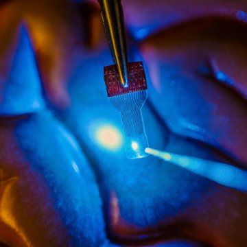
A blue light shines through a clear, implantable medical sensor onto a brain model. See-through sensors, which have been developed by a team of UW–Madison engineers, should help neural researchers better view brain activity. Credit: Justin Williams research group

A blue light shines through a clear, implantable medical sensor onto a brain model. See-through sensors, which have been developed by a team of UW–Madison engineers, should help neural researchers better view brain activity. Credit: Justin Williams research group

Read this Oct. 13, 2016 news item on ScienceDaily if you want to find out how to make your own transparent electronics,

When University of Wisconsin-Madison engineers announced in the journal Nature Communications that they had developed transparent sensors for use in imaging the brain, researchers around the world took notice.

Then the requests came flooding in. “So many research groups started asking us for these devices that we couldn’t keep up,” says Zhenqiang (Jack) Ma, the Lynn H. Matthias Professor and Vilas Distinguished Achievement Professor in electrical and computer engineering at UW-Madison.

As a result, in a paper published in the journal Nature Protocols, the researchers have described in great detail how to fabricate and use transparent graphene neural electrode arrays in applications in electrophysiology, fluorescent microscopy, optical coherence tomography, and optogenetics. “We described how to do these things so we can start working on the next generation,” says Ma.

Although he and collaborator Justin Williams, the Vilas Distinguished Achievement Professor in biomedical engineering and neurological surgery at UW-Madison, patented the technology through the Wisconsin Alumni Research Foundation, they saw its potential for advancements in research. “That little step has already resulted in an explosion of research in this field,” says Williams. “We didn’t want to keep this technology in our lab. We wanted to share it and expand the boundaries of its applications.”

An Oct. 13, 2016 University of Wisconsin-Madison news release, which originated the news item, provides more detail about the paper and the researchers,

‘This paper is a gateway for other groups to explore the huge potential from here,’ says Ma. ‘Our technology demonstrates one of the key in vivo applications of graphene. We expect more revolutionary research will follow in this interdisciplinary field.’

Ma’s group is a world leader in developing revolutionary flexible electronic devices. The see-through, implantable micro-electrode arrays were light years beyond anything ever created.

Here’s a link to and a citation for the paper,

Fabrication and utility of a transparent graphene neural electrode array for electrophysiology, in vivo imaging, and optogenetics by Dong-Wook Park, Sarah K Brodnick, Jared P Ness, Farid Atry, Lisa Krugner-Higby, Amelia Sandberg, Solomon Mikael, Thomas J Richner, Joseph Novello, Hyungsoo Kim, Dong-Hyun Baek, Jihye Bong, Seth T Frye, Sanitta Thongpang, Kyle I Swanson, Wendell Lake, Ramin Pashaie, Justin C Williams, & Zhenqiang Ma. Nature Protocols 11, 2201–2222 (2016) doi:10.1038/nprot.2016.127 Published online 13 October 2016

Of course this paper is open access. The team’s previous paper published in 2014 was featured here in an Oct. 23, 2014 posting.

Carbon nanotubes that can outperform silicon

According to a Sept. 2, 2016 news item on phys.org, researchers at the University of Wisconsin-Madison have produced carbon nanotube transistors that outperform state-of-the-art silicon transistors,

For decades, scientists have tried to harness the unique properties of carbon nanotubes to create high-performance electronics that are faster or consume less power—resulting in longer battery life, faster wireless communication and faster processing speeds for devices like smartphones and laptops.

But a number of challenges have impeded the development of high-performance transistors made of carbon nanotubes, tiny cylinders made of carbon just one atom thick. Consequently, their performance has lagged far behind semiconductors such as silicon and gallium arsenide used in computer chips and personal electronics.

Now, for the first time, University of Wisconsin-Madison materials engineers have created carbon nanotube transistors that outperform state-of-the-art silicon transistors.

Led by Michael Arnold and Padma Gopalan, UW-Madison professors of materials science and engineering, the team’s carbon nanotube transistors achieved current that’s 1.9 times higher than silicon transistors. …

A Sept. 2, 2016 University of Wisconsin-Madison news release (also on EurekAlert) by Adam Malecek, which originated the news item, describes the research in more detail and notes that the technology has been patented,

“This achievement has been a dream of nanotechnology for the last 20 years,” says Arnold. “Making carbon nanotube transistors that are better than silicon transistors is a big milestone. This breakthrough in carbon nanotube transistor performance is a critical advance toward exploiting carbon nanotubes in logic, high-speed communications, and other semiconductor electronics technologies.”

This advance could pave the way for carbon nanotube transistors to replace silicon transistors and continue delivering the performance gains the computer industry relies on and that consumers demand. The new transistors are particularly promising for wireless communications technologies that require a lot of current flowing across a relatively small area.

As some of the best electrical conductors ever discovered, carbon nanotubes have long been recognized as a promising material for next-generation transistors.

Carbon nanotube transistors should be able to perform five times faster or use five times less energy than silicon transistors, according to extrapolations from single nanotube measurements. The nanotube’s ultra-small dimension makes it possible to rapidly change a current signal traveling across it, which could lead to substantial gains in the bandwidth of wireless communications devices.

But researchers have struggled to isolate purely carbon nanotubes, which are crucial, because metallic nanotube impurities act like copper wires and disrupt their semiconducting properties — like a short in an electronic device.

The UW–Madison team used polymers to selectively sort out the semiconducting nanotubes, achieving a solution of ultra-high-purity semiconducting carbon nanotubes.

“We’ve identified specific conditions in which you can get rid of nearly all metallic nanotubes, where we have less than 0.01 percent metallic nanotubes,” says Arnold.

Placement and alignment of the nanotubes is also difficult to control.

To make a good transistor, the nanotubes need to be aligned in just the right order, with just the right spacing, when assembled on a wafer. In 2014, the UW–Madison researchers overcame that challenge when they announced a technique, called “floating evaporative self-assembly,” that gives them this control.

The nanotubes must make good electrical contacts with the metal electrodes of the transistor. Because the polymer the UW–Madison researchers use to isolate the semiconducting nanotubes also acts like an insulating layer between the nanotubes and the electrodes, the team “baked” the nanotube arrays in a vacuum oven to remove the insulating layer. The result: excellent electrical contacts to the nanotubes.

The researchers also developed a treatment that removes residues from the nanotubes after they’re processed in solution.

“In our research, we’ve shown that we can simultaneously overcome all of these challenges of working with nanotubes, and that has allowed us to create these groundbreaking carbon nanotube transistors that surpass silicon and gallium arsenide transistors,” says Arnold.

The researchers benchmarked their carbon nanotube transistor against a silicon transistor of the same size, geometry and leakage current in order to make an apples-to-apples comparison.

They are continuing to work on adapting their device to match the geometry used in silicon transistors, which get smaller with each new generation. Work is also underway to develop high-performance radio frequency amplifiers that may be able to boost a cellphone signal. While the researchers have already scaled their alignment and deposition process to 1 inch by 1 inch wafers, they’re working on scaling the process up for commercial production.

Arnold says it’s exciting to finally reach the point where researchers can exploit the nanotubes to attain performance gains in actual technologies.

“There has been a lot of hype about carbon nanotubes that hasn’t been realized, and that has kind of soured many people’s outlook,” says Arnold. “But we think the hype is deserved. It has just taken decades of work for the materials science to catch up and allow us to effectively harness these materials.”

The researchers have patented their technology through the Wisconsin Alumni Research Foundation.

Interestingly, at least some of the research was publicly funded according to the news release,

Funding from the National Science Foundation, the Army Research Office and the Air Force supported their work.

Will the public ever benefit financially from this research?

A treasure trove of molecule and battery data released to the public

Scientists working on The Materials Project have taken the notion of open science to their hearts and opened up access to their data according to a June 9, 2016 news item on Nanowerk,

The Materials Project, a Google-like database of material properties aimed at accelerating innovation, has released an enormous trove of data to the public, giving scientists working on fuel cells, photovoltaics, thermoelectrics, and a host of other advanced materials a powerful tool to explore new research avenues. But it has become a particularly important resource for researchers working on batteries. Co-founded and directed by Lawrence Berkeley National Laboratory (Berkeley Lab) scientist Kristin Persson, the Materials Project uses supercomputers to calculate the properties of materials based on first-principles quantum-mechanical frameworks. It was launched in 2011 by the U.S. Department of Energy’s (DOE) Office of Science.

A June 8, 2016 Berkeley Lab news release, which originated the news item, provides more explanation about The Materials Project,

The idea behind the Materials Project is that it can save researchers time by predicting material properties without needing to synthesize the materials first in the lab. It can also suggest new candidate materials that experimentalists had not previously dreamed up. With a user-friendly web interface, users can look up the calculated properties, such as voltage, capacity, band gap, and density, for tens of thousands of materials.

Two sets of data were released last month: nearly 1,500 compounds investigated for multivalent intercalation electrodes and more than 21,000 organic molecules relevant for liquid electrolytes as well as a host of other research applications. Batteries with multivalent cathodes (which have multiple electrons per mobile ion available for charge transfer) are promising candidates for reducing cost and achieving higher energy density than that available with current lithium-ion technology.

The sheer volume and scope of the data is unprecedented, said Persson, who is also a professor in UC Berkeley’s Department of Materials Science and Engineering. “As far as the multivalent cathodes, there’s nothing similar in the world that exists,” she said. “To give you an idea, experimentalists are usually able to focus on one of these materials at a time. Using calculations, we’ve added data on 1,500 different compositions.”

While other research groups have made their data publicly available, what makes the Materials Project so useful are the online tools to search all that data. The recent release includes two new web apps—the Molecules Explorer and the Redox Flow Battery Dashboard—plus an add-on to the Battery Explorer web app enabling researchers to work with other ions in addition to lithium.

“Not only do we give the data freely, we also give algorithms and software to interpret or search over the data,” Persson said.

The Redox Flow Battery app gives scientific parameters as well as techno-economic ones, so battery designers can quickly rule out a molecule that might work well but be prohibitively expensive. The Molecules Explorer app will be useful to researchers far beyond the battery community.

“For multivalent batteries it’s so hard to get good experimental data,” Persson said. “The calculations provide rich and robust benchmarks to assess whether the experiments are actually measuring a valid intercalation process or a side reaction, which is particularly difficult for multivalent energy technology because there are so many problems with testing these batteries.”

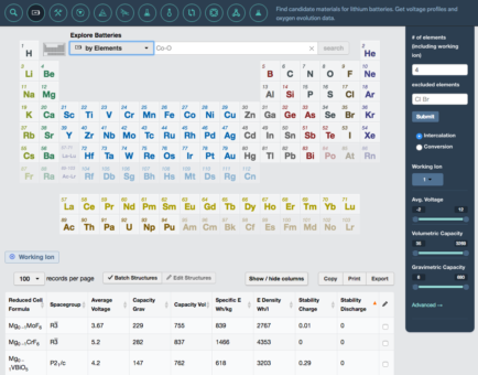
Here’s a screen capture from the Battery Explorer app,

The Materials Project’s Battery Explorer app now allows researchers to work with other ions in addition to lithium.

The Materials Project’s Battery Explorer app now allows researchers to work with other ions in addition to lithium. Courtesy: The Materials Project

The news release goes on to describe a new discovery made possible by The Materials Project (Note: A link has been removed),

Together with Persson, Berkeley Lab scientist Gerbrand Ceder, postdoctoral associate Miao Liu, and MIT graduate student Ziqin Rong, the Materials Project team investigated some of the more promising materials in detail for high multivalent ion mobility, which is the most difficult property to achieve in these cathodes. This led the team to materials known as thiospinels. One of these thiospinels has double the capacity of the currently known multivalent cathodes and was recently synthesized and tested in the lab by JCESR researcher Linda Nazar of the University of Waterloo, Canada.

“These materials may not work well the first time you make them,” Persson said. “You have to be persistent; for example you may have to make the material very phase pure or smaller than a particular particle size and you have to test them under very controlled conditions. There are people who have actually tried this material before and discarded it because they thought it didn’t work particularly well. The power of the computations and the design metrics we have uncovered with their help is that it gives us the confidence to keep trying.”

The researchers were able to double the energy capacity of what had previously been achieved for this kind of multivalent battery. The study has been published in the journal Energy & Environmental Science in an article titled, “A High Capacity Thiospinel Cathode for Mg Batteries.”

“The new multivalent battery works really well,” Persson said. “It’s a significant advance and an excellent proof-of-concept for computational predictions as a valuable new tool for battery research.”

Here’s a link to and a citation for the paper,

A high capacity thiospinel cathode for Mg batteries by Xiaoqi Sun, Patrick Bonnick, Victor Duffort, Miao Liu, Ziqin Rong, Kristin A. Persson, Gerbrand Ceder and  Linda F. Nazar. Energy Environ. Sci., 2016, Advance Article DOI: 10.1039/C6EE00724D First published online 24 May 2016

This paper seems to be behind a paywall.

Getting back to the news release, there’s more about The Materials Project in relationship to its membership,

The Materials Project has attracted more than 20,000 users since launching five years ago. Every day about 20 new users register and 300 to 400 people log in to do research.

One of those users is Dane Morgan, a professor of engineering at the University of Wisconsin-Madison who develops new materials for a wide range of applications, including highly active catalysts for fuel cells, stable low-work function electron emitter cathodes for high-powered microwave devices, and efficient, inexpensive, and environmentally safe solar materials.

“The Materials Project has enabled some of the most exciting research in my group,” said Morgan, who also serves on the Materials Project’s advisory board. “By providing easy access to a huge database, as well as tools to process that data for thermodynamic predictions, the Materials Project has enabled my group to rapidly take on materials design projects that would have been prohibitive just a few years ago.”

More materials are being calculated and added to the database every day. In two years, Persson expects another trove of data to be released to the public.

“This is the way to reach a significant part of the research community, to reach students while they’re still learning material science,” she said. “It’s a teaching tool. It’s a science tool. It’s unprecedented.”

Supercomputing clusters at the National Energy Research Scientific Computing Center (NERSC), a DOE Office of Science User Facility hosted at Berkeley Lab, provide the infrastructure for the Materials Project.

Funding for the Materials Project is provided by the Office of Science (US Department of Energy], including support through JCESR [Joint Center for Energy Storage Research].

Happy researching!

Science literacy, science advice, the US Supreme Court, and Britain’s House of Commons

This ‘think’ piece is going to cover a fair bit of ground including science literacy in the general public and in the US Supreme Court, and what that might mean for science advice and UK Members of Parliament (MPs).

Science literacy generally and in the US Supreme Court

A science literacy report for the US National Academy of Sciences (NAS), due sometime from early to mid 2017, is being crafted with an eye to capturing a different perspective according to a March 24, 2016 University of Wisconsin-Madison news release by Terry Dewitt,

What does it mean to be science literate? How science literate is the American public? How do we stack up against other countries? What are the civic implications of a public with limited knowledge of science and how it works? How is science literacy measured?

These and other questions are under the microscope of a 12-member National Academy of Sciences (NAS) panel — including University of Wisconsin—Madison Life Sciences Communication Professor Dominique Brossard and School of Education Professor Noah Feinstein — charged with sorting through the existing data on American science and health literacy and exploring the association between knowledge of science and public perception of and support for science.

The committee — composed of educators, scientists, physicians and social scientists — will take a hard look at the existing data on the state of U.S. science literacy, the questions asked, and the methods used to measure what Americans know and don’t know about science and how that knowledge has changed over time. Critically for science, the panel will explore whether a lack of science literacy is associated with decreased public support for science or research.

Historically, policymakers and leaders in the scientific community have fretted over a perceived lack of knowledge among Americans about science and how it works. A prevailing fear is that an American public unequipped to come to terms with modern science will ultimately have serious economic, security and civic consequences, especially when it comes to addressing complex and nuanced issues like climate change, antibiotic resistance, emerging diseases, environment and energy choices.

While the prevailing wisdom, inspired by past studies, is that Americans don’t stack up well in terms of understanding science, Brossard is not so convinced. Much depends on what kinds of questions are asked, how they are asked, and how the data is analyzed.

It is very easy, she argues, to do bad social science and past studies may have measured the wrong things or otherwise created a perception about the state of U.S. science literacy that may or may not be true.

“How do you conceptualize scientific literacy? What do people need to know? Some argue that scientific literacy may be as simple as an understanding of how science works, the nature of science, [emphasis mine]” Brossard explains. “For others it may be a kind of ‘civic science literacy,’ where people have enough knowledge to be informed and make good decisions in a civics context.”

Science literacy may not be just for the public, it would seem that US Supreme Court judges may not have a basic understanding of how science works. David Bruggeman’s March 24, 2016 posting (on his Pasco Phronesis blog) describes a then current case before the Supreme Court (Justice Antonin Scalia has since died), Note: Links have been removed,

It’s a case concerning aspects of the University of Texas admissions process for undergraduates and the case is seen as a possible means of restricting race-based considerations for admission.  While I think the arguments in the case will likely revolve around factors far removed from science and or technology, there were comments raised by two Justices that struck a nerve with many scientists and engineers.

Both Justice Antonin Scalia and Chief Justice John Roberts raised questions about the validity of having diversity where science and scientists are concerned [emphasis mine].  Justice Scalia seemed to imply that diversity wasn’t esential for the University of Texas as most African-American scientists didn’t come from schools at the level of the University of Texas (considered the best university in Texas).  Chief Justice Roberts was a bit more plain about not understanding the benefits of diversity.  He stated, “What unique perspective does a black student bring to a class in physics?”

To that end, Dr. S. James Gates, theoretical physicist at the University of Maryland, and member of the President’s Council of Advisers on Science and Technology (and commercial actor) has an editorial in the March 25 [2016] issue of Science explaining that the value of having diversity in science does not accrue *just* to those who are underrepresented.

Dr. Gates relates his personal experience as a researcher and teacher of how people’s background inform their practice of science, and that two different people may use the same scientific method, but think about the problem differently.

I’m guessing that both Scalia and Roberts and possibly others believe that science is the discovery and accumulation of facts. In this worldview science facts such as gravity are waiting for discovery and formulation into a ‘law’. They do not recognize that most science is a collection of beliefs and may be influenced by personal beliefs. For example, we believe we’ve proved the existence of the Higgs boson but no one associated with the research has ever stated unequivocally that it exists.

For judges who are under the impression that scientific facts are out there somewhere waiting to be discovered diversity must seem irrelevant. It is not. Who you are affects the questions you ask and how you approach science. The easiest example is to look at how women were viewed when they were subjects in medical research. The fact that women’s physiology is significantly different (and not just in child-bearing ways) was never considered relevant when reporting results. Today, researchers consider not only gender, but age (to some extent), ethnicity, and more when examining results. It’s still not a perfect but it was a step forward.

So when Brossard included “… an understanding of how science works, the nature of science …” as an aspect of science literacy, the judges seemed to present a good example of how not understanding science can have a major impact on how others live.

I’d almost forgotten this science literacy piece as I’d started the draft some months ago but then I spotted a news item about a science advice/MP ‘dating’ service in the UK.

Science advice and UK MPs

First, the news, then, the speculation (from a June 6, 2016 news item on ScienceDaily),

MPs have expressed an overwhelming willingness to use a proposed new service to swiftly link them with academics in relevant areas to help ensure policy is based on the latest evidence.

A June 6, 2016 University of Exeter press release, which originated the news item, provides more detail about the proposed service and the research providing the supporting evidence (Note: A link has been removed),

The government is pursuing a drive towards evidence-based policy, yet policy makers still struggle to incorporate evidence into their decisions. One reason for this is limited easy access to the latest research findings or to academic experts who can respond to questions about evidence quickly.

Researchers at Cardiff University, the University of Exeter and University College London have today published results of the largest study to date reporting MPs’ attitudes to evidence in policy making and their reactions to a proposed Evidence Information Service (EIS) – a rapid match-making advisory service that would work alongside existing systems to put MPs in touch with relevant academic experts.

Dr Natalia Lawrence, of the University of Exeter, said: “It’s clear from our study that politicians want to ensure their decisions incorporate the most reliable evidence, but it can sometimes be very difficult for them to know how to access the latest research findings. This new matchmaking service could be a quick and easy way for them to seek advice from cutting-edge researchers and to check their understanding and facts. It could provide a useful complement to existing highly-valued information services.”

The research, published today in the journal Evidence and Policy, reports the findings of a national consultation exercise between politicians and the public. The researchers recruited members of the public to interview their local parliamentary representative. In total 86, politicians were contacted with 56 interviews completed. The MPs indicated an overwhelming willingness to use a service such as the EIS, with 85% supporting the idea, but noted a number of potential reservations related to the logistics of the EIS such as response time and familiarity with the service. Yet, the MPs indicated that their logistical reservations could be overcome by accessing the EIS via existing highly-valued parliamentary information services such as those provided by the House of Commons and Lords Libraries. Furthermore prior to rolling out the EIS on a nationwide basis it would first need to be piloted.

Developing the proposed EIS in line with feedback from this consultation of MPs would offer the potential to provide policy makers with rapid, reliable and confidential evidence from willing volunteers from the research community.

Professor Chris Chambers, of Cardiff University, said: “The government has given a robust steer that MPs need to link in more with academics to ensure decisions shaping the future of the country are evidence-based. It’s heartening to see that there is a will to adopt this system and we now need to move into a phase of developing a service that is both simple and effective to meet this need.”

The next steps for the project are parallel consultations of academics and members of the public and a pilot of the EIS, using funding from GW4 alliance of universities, made up of Bath, Bristol, Cardiff and Exeter.

What this study shows:
• The consultation shows that politicians recognise the importance of evidence-based policy making and agree on the need for an easier and more direct linkage between academic experts and policy makers.
• Politicians would welcome the creation of the EIS as a provider of rapid, reliable and confidential evidence.

What this study does not show:
• This study does not show how academics would provide evidence. This was a small-scale study which consulted politicians and has not attempted to give voice to the academic community.
• This study does not detail the mechanism of an operational EIS. Instead it indicates the need for a service such as the EIS and suggests ways in which the EIS can be operationalized.

Here’s a link to and a citation for the paper,

Service as a new platform for supporting evidence-based policy: a consultation of UK parliamentarians by Natalia Lawrence, Jemma Chambers, Sinead Morrison, Sven Bestmann, Gerard O’Grady, Christopher Chambers, Andrew Kythreotis. Evidence & Policy: A Journal of Research, Debate and Practice DOI: http://dx.doi.org/10.1332/174426416X14643531912169 Appeared or available online: June 6, 2016

This paper is behind a paywall open access. *Corrected June 17, 2016.*

It’s an interesting idea and I can understand the appeal. However, operationalizing this ‘dating’ or ‘matchmaking’ service could prove quite complex. I appreciate the logistics issues but I’m a little more concerned about the MPs’ science literacy. Are they going to be like the two US justices who believe that science is the pursuit of immutable facts? What happens if two MPs are matched up with a different scientist and those two scientists didn’t agree about what the evidence says. Or, what happens if one scientist is more cautious than the other. There are all kinds of pitfalls. I’m not arguing against the idea but it’s going to require a lot of careful consideration.
Diamond-based electronics?

A May 24, 2016 news item on ScienceDaily describes the latest research on using diamonds as semiconductors,

Along with being a “girl’s best friend,” diamonds also have remarkable properties that could make them ideal semiconductors. This is welcome news for electronics; semiconductors are needed to meet the rising demand for more efficient electronics that deliver and convert power.

The thirst for electronics is unlikely to cease and almost every appliance or device requires a suite of electronics that transfer, convert and control power. Now, researchers have taken an important step toward that technology with a new way to dope single crystals of diamonds, a crucial process for building electronic devices.

A May 24, 2016 American Institute of Physics (AIP) news release (also on EurekAlert), which originated the news item, provides more detail,

For power electronics, diamonds could serve as the perfect material. They are thermally conductive, which means diamond-based devices would dissipate heat quickly and easily, foregoing the need for bulky and expensive methods for cooling. Diamond can also handle high voltages and power. Electrical currents also flow through diamonds quickly, meaning the material would make for energy efficient devices.

But among the biggest challenges to making diamond-based devices is doping, a process in which other elements are integrated into the semiconductor to change its properties. Because of diamond’s rigid crystalline structure, doping is difficult.

Currently, you can dope diamond by coating the crystal with boron and heating it to 1450 degrees Celsius. But it’s difficult to remove the boron coating at the end. This method only works on diamonds consisting of multiple crystals stuck together. Because such polydiamonds have irregularities between the crystals, single-crystals would be superior semiconductors.

You can dope single crystals by injecting boron atoms while growing the crystals artificially. The problem is the process requires powerful microwaves that can degrade the quality of the crystal.

Now, Ma [Zhengqiang (Jack) Ma, an electrical and computer engineering professor at the University of Wisconsin-Madison] and his colleagues have found a way to dope single-crystal diamonds with boron at relatively low temperatures and without any degradation. The researchers discovered if you bond a single-crystal diamond with a piece of silicon doped with boron, and heat it to 800 degrees Celsius, which is low compared to the conventional techniques, the boron atoms will migrate from the silicon to the diamond. It turns out that the boron-doped silicon has defects such as vacancies, where an atom is missing in the lattice structure. Carbon atoms from the diamond will fill those vacancies, leaving empty spots for boron atoms.

This technique also allows for selective doping, which means more control when making devices. You can choose where to dope a single-crystal diamond simply by bonding the silicon to that spot.

The new method only works for P-type doping, where the semiconductor is doped with an element that provides positive charge carriers (in this case, the absence of electrons, called holes).

“We feel like we found a very easy, inexpensive, and effective way to do it,” Ma said. The researchers are already working on a simple device using P-type single-crystal diamond semiconductors.

But to make electronic devices like transistors, you need N-type doping that gives the semiconductor negative charge carriers (electrons). And other barriers remain. Diamond is expensive and single crystals are very small.

Still, Ma says, achieving P-type doping is an important step, and might inspire others to find solutions for the remaining challenges. Eventually, he said, single-crystal diamond could be useful everywhere — perfect, for instance, for delivering power through the grid.

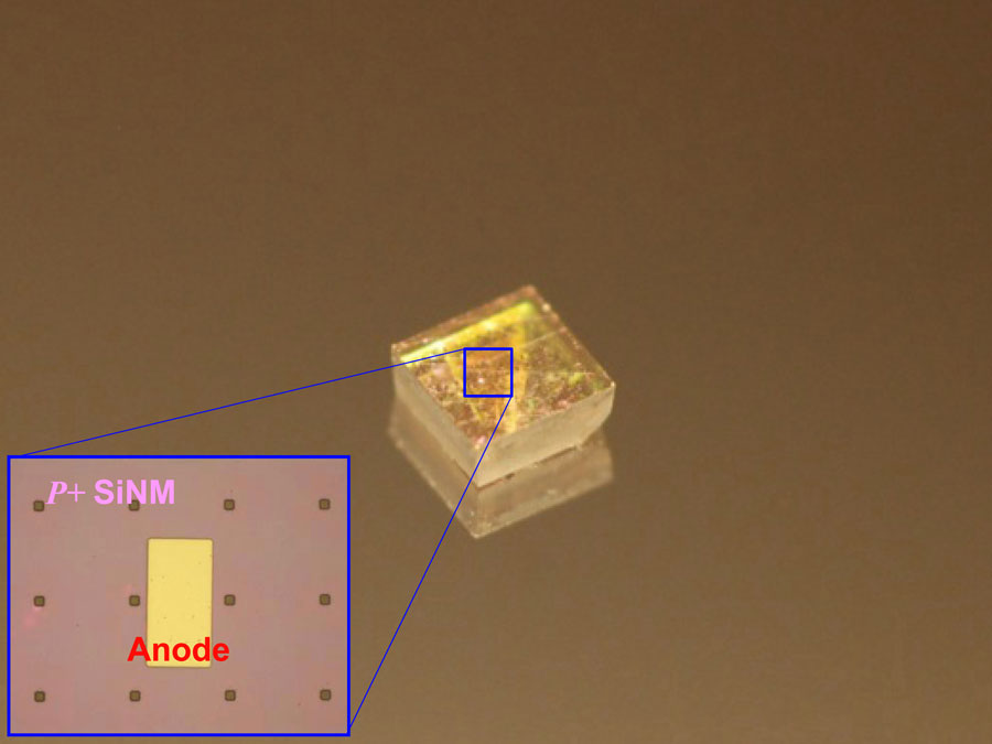
Here’s an image the researchers have released,

Optical image of a diode array on a natural single crystalline diamond plate. (The image looks blurred due to light scattering by the array of small pads on top of the diamond plate.) Inset shows the deposited anode metal on top of heavy doped Si nanomembrane that is bonded to natural single crystalline diamond. CREDIT: Jung-Hun Seo

Optical image of a diode array on a natural single crystalline diamond plate. (The image looks blurred due to light scattering by the array of small pads on top of the diamond plate.) Inset shows the deposited anode metal on top of heavy doped Si nanomembrane that is bonded to natural single crystalline diamond. CREDIT: Jung-Hun Seo Courtesy: American Institute of Physics

Here’s a link to and a citation for the paper,

Thermal diffusion boron doping of single-crystal natural diamond by Jung-Hun Seo, Henry Wu, Solomon Mikael, Hongyi Mi, James P. Blanchard, Giri Venkataramanan, Weidong Zhou, Shaoqin Gong, Dane Morgan, and Zhenqiang Ma. J. Appl. Phys. 119, 205703 (2016); http://dx.doi.org/10.1063/1.4949327

This paper appears to be open access.

$5.2M in nanotechnology grants from the US Department of Agriculture (USDA)

A March 30, 2016 news item on Nanowerk announces the 2016 nanotechnology grants from the US Dept. of Agriculture (USDA),

Agriculture Secretary Tom Vilsack today [March 30, 2016] announced an investment of more than $5.2 million to support nanotechnology research at 11 universities. The universities will research ways nanotechnology can be used to improve food safety, enhance renewable fuels, increase crop yields, manage agricultural pests, and more. The awards were made through the Agriculture and Food Research Initiative (AFRI), the nation’s premier competitive, peer-reviewed grants program for fundamental and applied agricultural sciences.

A March 30, 2016 USDA news release provides more detail,

“In the seven years since the Agriculture and Food Research Initiative was established, the program has led to true innovations and ground-breaking discoveries in agriculture to combat childhood obesity, improve and sustain rural economic growth, address water availability issues, increase food production, find new sources of energy, mitigate the impacts of climate variability and enhance resiliency of our food systems, and ensure food safety. Nanoscale science, engineering, and technology are key pieces of our investment in innovation to ensure an adequate and safe food supply for a growing global population,” said Vilsack. “The President’s 2017 Budget calls for full funding of the Agriculture and Food Research Initiative so that USDA can continue to support important projects like these.”

Universities receiving funding include Auburn University in Auburn, Ala.; Connecticut Agricultural Experiment Station in New Haven, Conn.; University of Central Florida in Orlando, Fla; University of Georgia in Athens, Ga.; Iowa State University in Ames, Iowa; University of Massachusetts in Amherst, Mass.; Mississippi State University in Starkville, Miss.; Lincoln University in Jefferson City, Mo.; Clemson University in Clemson, S.C.; Virginia Polytechnic Institute and State University in Blacksburg, Va.; and University of Wisconsin in Madison, Wis.

With this funding, Auburn University proposes to improve pathogen monitoring throughout the food supply chain by creating a user-friendly system that can detect multiple foodborne pathogens simultaneously, accurately, cost effectively, and rapidly. Mississippi State University will research ways nanochitosan can be used as a combined fire-retardant and antifungal wood treatment that is also environmentally safe. Experts in nanotechnology, molecular biology, vaccines and poultry diseases at the University of Wisconsin will work to develop nanoparticle-based poultry vaccines to prevent emerging poultry infections. USDA has a full list of projects and longer descriptions available online.

Past projects include a University of Georgia project developing a bio-nanocomposites-based, disease-specific, electrochemical sensors for detecting fungal pathogen induced volatiles in selected crops; and a University of Massachusetts project creating a platform for pathogen detection in foods that is superior to the current detection method in terms of analytical time, sensitivity, and accuracy using a novel, label-free, surface-enhanced Raman scattering (SERS) mapping technique.

The purpose of AFRI is to support research, education, and extension work by awarding grants that address key problems of national, regional, and multi-state importance in sustaining all components of food and agriculture. AFRI is the flagship competitive grant program administered by USDA’s National Institute of Food and Agriculture [NIFA]. Established under the 2008 Farm Bill, AFRI supports work in six priority areas: plant health and production and plant products; animal health and production and animal products; food safety, nutrition and health; bioenergy, natural resources and environment; agriculture systems and technology; and agriculture economics and rural communities. Since AFRI’s creation, NIFA has awarded more than $89 million to solve challenges related to plant health and production; $22 million of this has been dedicated to nanotechnology research. The President’s 2017 budget request proposes to fully fund AFRI for $700 million; this amount is the full funding level authorized by Congress when it established AFRI in the 2008 Farm Bill.

Each day, the work of USDA scientists and researchers touches the lives of all Americans: from the farm field to the kitchen table and from the air we breathe to the energy that powers our country. USDA science is on the cutting edge, helping to protect, secure, and improve our food, agricultural and natural resources systems. USDA research develops and transfers solutions to agricultural problems, supporting America’s farmers and ranchers in their work to produce a safe and abundant food supply for more than 100 years. This work has helped feed the nation and sustain an agricultural trade surplus since the 1960s. Since 2009, USDA has invested $4.32 billion in research and development grants. Studies have shown that every dollar invested in agricultural research now returns over $20 to our economy.

Since 2009, NIFA has invested in and advanced innovative and transformative initiatives to solve societal challenges and ensure the long-term viability of agriculture. NIFA’s integrated research, education, and extension programs, supporting the best and brightest scientists and extension personnel, have resulted in user-inspired, groundbreaking discoveries that are combating childhood obesity, improving and sustaining rural economic growth, addressing water availability issues, increasing food production, finding new sources of energy, mitigating climate variability, and ensuring food safety.

Center for Sustainable Nanotechnology or how not to poison and make the planet uninhabitable

I received notice of the Center for Sustainable Nanotechnology’s newest deal with the US National Science Foundation in an August 31, 2015 email University of Wisconsin-Madison (UWM) news release,

The Center for Sustainable Nanotechnology, a multi-institutional research center based at the University of Wisconsin-Madison, has inked a new contract with the National Science Foundation (NSF) that will provide nearly $20 million in support over the next five years.

Directed by UW-Madison chemistry Professor Robert Hamers, the center focuses on the molecular mechanisms by which nanoparticles interact with biological systems.

Nanotechnology involves the use of materials at the smallest scale, including the manipulation of individual atoms and molecules. Products that use nanoscale materials range from beer bottles and car wax to solar cells and electric and hybrid car batteries. If you read your books on a Kindle, a semiconducting material manufactured at the nanoscale underpins the high-resolution screen.

While there are already hundreds of products that use nanomaterials in various ways, much remains unknown about how these modern materials and the tiny particles they are composed of interact with the environment and living things.

“The purpose of the center is to explore how we can make sure these nanotechnologies come to fruition with little or no environmental impact,” explains Hamers. “We’re looking at nanoparticles in emerging technologies.”

In addition to UW-Madison, scientists from UW-Milwaukee, the University of Minnesota, the University of Illinois, Northwestern University and the Pacific Northwest National Laboratory have been involved in the center’s first phase of research. Joining the center for the next five-year phase are Tuskegee University, Johns Hopkins University, the University of Iowa, Augsburg College, Georgia Tech and the University of Maryland, Baltimore County.

At UW-Madison, Hamers leads efforts in synthesis and molecular characterization of nanomaterials. soil science Professor Joel Pedersen and chemistry Professor Qiang Cui lead groups exploring the biological and computational aspects of how nanomaterials affect life.

Much remains to be learned about how nanoparticles affect the environment and the multitude of organisms – from bacteria to plants, animals and people – that may be exposed to them.

“Some of the big questions we’re asking are: How is this going to impact bacteria and other organisms in the environment? What do these particles do? How do they interact with organisms?” says Hamers.

For instance, bacteria, the vast majority of which are beneficial or benign organisms, tend to be “sticky” and nanoparticles might cling to the microorganisms and have unintended biological effects.

“There are many different mechanisms by which these particles can do things,” Hamers adds. “The challenge is we don’t know what these nanoparticles do if they’re released into the environment.”

To get at the challenge, Hamers and his UW-Madison colleagues are drilling down to investigate the molecular-level chemical and physical principles that dictate how nanoparticles interact with living things.
Pedersen’s group, for example, is studying the complexities of how nanoparticles interact with cells and, in particular, their surface membranes.

“To enter a cell, a nanoparticle has to interact with a membrane,” notes Pedersen. “The simplest thing that can happen is the particle sticks to the cell. But it might cause toxicity or make a hole in the membrane.”

Pedersen’s group can make model cell membranes in the lab using the same lipids and proteins that are the building blocks of nature’s cells. By exposing the lab-made membranes to nanomaterials now used commercially, Pedersen and his colleagues can see how the membrane-particle interaction unfolds at the molecular level – the scale necessary to begin to understand the biological effects of the particles.

Such studies, Hamers argues, promise a science-based understanding that can help ensure the technology leaves a minimal environmental footprint by identifying issues before they manifest themselves in the manufacturing, use or recycling of products that contain nanotechnology-inspired materials.

To help fulfill that part of the mission, the center has established working relationships with several companies to conduct research on materials in the very early stages of development.

“We’re taking a look-ahead view. We’re trying to get into the technological design cycle,” Hamers says. “The idea is to use scientific understanding to develop a predictive ability to guide technology and guide people who are designing and using these materials.”

What with this initiative and the LCnano Network at Arizona State University (my April 8, 2014 posting; scroll down about 50% of the way), it seems that environmental and health and safety studies of nanomaterials are kicking into a higher gear as commercialization efforts intensify.

Audience perceptions of emerging technologies and media stories that emphasize conflict over nuance

A few names popped into my head, as soon as I saw a news release focused on audience perceptions and emerging technologies. I was right about one of the authors (Dominique Brossard of the University of Wisconsin-Madison [UWM] often writes on the topic) however, the lead author is Andrew Binder of North Carolina State University (NCSU). An August 31, 2015 NCSU news release describes a joint NCSU-UWM research project  (Note: Links have been removed),

Researchers from NC State University and the University of Wisconsin-Madison have found more evidence that how media report on emerging technologies – such as nanotechnology or genetically modified crops – influences public opinion on those subjects.

Specifically, when news stories highlight conflict in the scientific community on an emerging technology, people who accept the authority of scientists on scientific subjects are more likely to view the emerging technology as risky.

“Scientists – even scientists who disagree – often incorporate caveats and nuance into their comments on emerging technologies,” says Andrew R. Binder, lead author of a paper on the work and an associate professor of communication at NC State. “For example, a scientist may voice an opinion but note a lack of data on the subject. But that nuance is often lost in news stories.

“We wanted to know stories that present scientists as being in clear conflict, leaving out the nuance, affected the public’s perception of uncertainty on an issue – particularly compared to stories that incorporate the nuances of each scientist’s position,” Binder says.

For their experiment, the researchers had 250 college students answer a questionnaire on their deference to scientific authority and their perceptions of nanotechnology. Participants were split into four groups. Before asking about nanotechnology, one group was asked to read a news story about nanotech that quoted scientists and presented them as being in conflict; one group read a news story with quotes that showed disagreement between scientists but included nuance on each scientist’s position; one group read a story without quotes; and one group – the control group – was given no reading.

In most instances, the reading assignments did not have a significant impact on study participants’ perception of risks associated with nanotechnology. However, those participants who were both “highly deferent” to scientific authority and given the “conflict” news item perceived nanotechnology as being significantly more risky as compared to those highly deferent study participants who read the “nuance” article.

“One thing that’s interesting here is that participants who were highly deferential to scientific authority but were in the control group or read the news item without quotes – they landed about halfway between the ‘conflict’ group and the ‘nuance’ group,” Binder says. “So it would seem that the way reporters frame scientific opinion can sway an audience one way or the other.”

The researchers also found that, while an appearance of conflict can increase one’s perception of risk, it did not increase participants’ sense of certainty in their position.

As a practical matter, the findings raise questions for journalists – since scientists have limited control over how they’re portrayed in the news. Previous surveys have found that many people are deferent to scientific authority – they trust scientists – so a reporter’s decision to cut nuance or highlight conflict could make a very real impact on how the public perceives emerging technologies.

“Reporters can’t include every single detail, and scientists want to include everything,” Binder says. “So I don’t think there’s a definitive solution out there that will make everyone happy. But hopefully this will encourage both parties to meet in the middle.”

I have one comment, this research was conducted on college students whose age range is likely more restricted than what you’d find in the general populace. I don’t know if the research team has plans or more funding but it would seem the next step would be to tested a wider range to see if the results with the college students can be generalized.

Here’s a link to and a citation for the paper,

Conflict or Caveats? Effects of Media Portrayals of Scientific Uncertainty on Audience Perceptions of New Technologies by Andrew R. Binder, Elliott D. Hillback, and Dominique Brossard. Risk Analysis DOI: 10.1111/risa.12462 Article first published online: 13 AUG 2015

© 2015 Society for Risk Analysis

This paper is behind a paywall.

Nanoscale device emits light as powerfully as an object 10,000 times its size

The potential application in the field of solar power is what most interests me in this collaborative research from the University of Wisconsin-Madison (US) and Fudan University in China. From a July 13, 2015 news item on ScienceDaily,

University of Wisconsin-Madison engineers have created a nanoscale device that can emit light as powerfully as an object 10,000 times its size. It’s an advance that could have huge implications for everything from photography to solar power.

In a paper published July 10 [2015] in the journal Physical Review Letters, Zongfu Yu, an assistant professor of electrical and computer engineering, and his collaborators describe a nanoscale device that drastically surpasses previous technology in its ability to scatter light. They showed how a single nanoresonator can manipulate light to cast a very large “reflection.” The nanoresonator’s capacity to absorb and emit light energy is such that it can make itself — and, in applications, other very small things — appear 10,000 times as large as its physical size.

A July 13, 2015 University of Wisconsin-Madison news release (also on EurekAlert) by Scott Gordon, which originated the news item, expands on the theme,

“Making an object look 10,000 times larger than its physical size has lots of implications in technologies related to light,” Yu says.

The researchers realized the advance through materials innovation and a keen understanding of the physics of light. Much like sound, light can resonate, amplifying itself as the surrounding environment manipulates the physical properties of its wave energy. The researchers took advantage of this by creating an artificial material in which the wavelength of light is much larger than in a vacuum, which allows light waves to resonate more powerfully.

The device condenses light to a size smaller than its wavelength, meaning it can gather a lot of light energy, and then scatters the light over a very large area, harnessing its output for imaging applications that make microscopic particles appear huge.

“The device makes an object super-visible by enlarging its optical appearance with this super-strong scattering effect,” says Ming Zhou, a Ph.D. student in Yu’s group and lead author of the paper.

Much as a very thin string on a guitar can absorb a large amount of acoustic energy from its surroundings and begin to vibrate in sympathy, this one very small optical device can receive light energy from all around and yield a surprisingly strong output. In imaging, this presents clear advantages over conventional lenses, whose light-gathering capacity is limited by direction and size.

“We are developing photodetectors based on this technology and, for example, it could be helpful for photographers wanting to shoot better quality pictures in weak light conditions,” Yu says.

Given the nanoresonator’s capacity to absorb large amounts of light energy, the technology also has potential in applications that harvest the sun’s energy with high efficiency. In addition, Yu envisions simply letting the resonator emit that energy in the form of infrared light toward the sky, which is very cold. Because the nanoresonator has a large optical cross-section — that is, an ability to emit light that dramatically exceeds its physical size — it can shed a lot of heat energy, making for a passive cooling system.

“This research opens up a new way to manipulate the flow of light, and could enable new technologies in light sensing and solar energy conversion,” Yu says.

Here’s a link to and a citation for the paper,

Extraordinarily Large Optical Cross Section for Localized Single Nanoresonator by Ming Zhou, Lei Shi, Jian Zi, and Zongfu Yu. Phys. Rev. Lett. 115, 023903  DOI: http://dx.doi.org/10.1103/PhysRevLett.115.023903 Published 10 July 2015

This paper is behind a paywall.

Cellulose Nanofibrillated Fiber Based Transistors from the University of Wisconsin-Madison

There’s a team of researchers at the University of Wisconsin-Madison working to substitute silicon used in computer chips with cellulose derived from wood (my May 27, 2015 posting). Their latest effort, featuring mobile electronics, is described in a July 1, 2015 news item on Azonano,

A report published by the U.S. Environmental Protection Agency in 2012 showed that about 152 million mobile devices are discarded every year, of which only 10 percent is recycled — a legacy of waste that consumes a tremendous amount of natural resources and produces a lot of trash made from expensive and non-biodegradable materials like highly purified silicon.

Now researchers from the University of Wisconsin-Madison have come up with a new solution to alleviate the environmental burden of discarded electronics. They have demonstrated the feasibility of making microwave biodegradable thin-film transistors from a transparent, flexible biodegradable substrate made from inexpensive wood, called cellulose nanofibrillated fiber (CNF). This work opens the door for green, low-cost, portable electronic devices in future.

A June 30, 2015 American Institute of Physics news release by Zhengzheng Zhang, which originated the news item, describes the research in more detail,

“We found that cellulose nanofibrillated fiber based transistors exhibit superior performance as that of conventional silicon-based transistors,” said Zhenqiang Ma, the team leader and a professor of electrical and computer engineering at the UW-Madison. “And the bio-based transistors are so safe that you can put them in the forest, and fungus will quickly degrade them. They become as safe as fertilizer.”

Nowadays, the majority of portable electronics are built on non-renewable, non-biodegradable materials such as silicon wafers, which are highly purified, expensive and rigid substrates, but cellulose nanofibrillated fiber films have the potential to replace silicon wafers as electronic substrates in environmental friendly, low-cost, portable gadgets or devices of the future.

Cellulose nanofibrillated fiber is a sustainable, strong, transparent nanomaterial made from wood. Compared to other polymers like plastics, the wood nanomaterial is biocompatible and has relatively low thermal expansion coefficient, which means the material won’t change shape as the temperature changes. All these superior properties make cellulose nanofibril an outstanding candidate for making portable green electronics.

To create high-performance devices, Ma’s team employed silicon nanomembranes as the active material in the transistor — pieces of ultra-thin films (thinner than a human hair) peeled from the bulk crystal and then transferred and glued onto the cellulose nanofibrill substrate to create a flexible, biodegradable and transparent silicon transistor.To create high-performance devices, Ma’s team employed silicon nanomembranes as the active material in the transistor — pieces of ultra-thin films (thinner than a human hair) peeled from the bulk crystal and then transferred and glued onto the cellulose nanofibrill substrate to create a flexible, biodegradable and transparent silicon transistor.

But to make portable electronics, the biodegradable transistor needed to be able to operate at microwave frequencies, which is the working range of most wireless devices. The researchers thus conducted a series of experiments such as measuring the current-voltage characteristics to study the device’s functional performance, which finally showed the biodegradable transistor has superior microwave-frequency operation capabilities comparable to existing semiconductor transistors.

“Biodegradable electronics provide a new solution for environmental problems brought by consumers’ pursuit of quickly upgraded portable devices,” said Ma. “It can be anticipated that future electronic chips and portable devices will be much greener and cheaper than that of today.”

Next, Ma and colleagues plan to develop more complicated circuit system based on the biodegradable transistors.

Here’s a link to and a citation for the team’s latest paper,

Microwave flexible transistors on cellulose nanofibrillated fiber substrates by Jung-Hun Seo, Tzu-Hsuan Chang, Jaeseong Lee, Ronald Sabo, Weidong Zhou, Zhiyong Cai, Shaoqin Gong, and Zhenqiang Ma.  Applied Physics Letters, Volume 106, Issue 26 or  Appl. Phys. Lett. 106, 262101 (2015); http://dx.doi.org/10.1063/1.4921077

This is an open access paper.