For a long time It seemed as if every country in the world, except Canada, had some some sort of graphene event. According to a July 16, 2015 news item on Nanotechnology Now, Canada has now stepped up, albeit, in a peculiarly Canadian fashion. First the news,
Mid October [Oct. 14 -16, 2015], the Graphene & 2D Materials Canada 2015 International Conference & Exhibition (www.graphenecanada2015.com) will take place in Montreal (Canada).
I found a July 16, 2015 news release (PDF) announcing the Canadian event on the lead organizer’s (Phantoms Foundation located in Spain) website,
On the second day of the event (15th October, 2015), an Industrial Forum will bring together top industry leaders to discuss recent advances in technology developments and business opportunities in graphene commercialization.
At this stage, the event unveils 38 keynote & invited speakers. On the Industrial Forum 19 of them will present the latest in terms of Energy, Applications, Production and Worldwide Initiatives & Priorities.
Plenary:
Gary Economo (Grafoid Inc., Canada)
Khasha Ghaffarzadeh (IDTechEx, UK)
Shu-Jen Han (IBM T.J. Watson Research Center, USA)
Bor Z. Jang (Angstron Materials, USA)
Seongjun Park (Samsung Advanced Institute of Technology (SAIT), Korea)
Chun-Yun Sung (Lockheed Martin, USA)
Parallel Sessions:
Gordon Chiu (Grafoid Inc., Canada)
Jesus de la Fuente (Graphenea, Spain)
Mark Gallerneault (ALCERECO Inc., Canada)
Ray Gibbs (Haydale Graphene Industries, UK)
Masataka Hasegawa (AIST, Japan)
Byung Hee Hong (SNU & Graphene Square, Korea)
Tony Ling (Jestico + Whiles, UK)
Carla Miner (SDTC, Canada)
Gregory Pognon (THALES Research & Technology, France)
Elena Polyakova (Graphene Laboratories Inc, USA)
Federico Rosei (INRS–EMT, Université du Québec, Canada)
Aiping Yu (University of Waterloo, Canada)
Hua Zhang (MSE-NTU, Singapore)
Apart from the industrial forum, several industry-related activities will be organized:
– Extensive thematic workshops in parallel (Standardization, Materials & Devices Characterization, Bio & Health and Electronic Devices)
– An exhibition carried out with the latest graphene trends (Grafoid, RAYMOR NanoIntegris, Nanomagnetics Instruments, ICEX and Xerox Research Centre of Canada (XRCC) already confirmed)
– B2B meetings to foster technical cooperation in the field of Graphene
It’s still possible to contribute to the event with an oral presentation. The call for abstracts is open until July, 20 [2015]. [emphasis mine]
Graphene Canada 2015 is already supported by Canada’s leading graphene applications developer, Grafoid Inc., Tourisme Montréal and Université de Montréal.
This is what makes the event peculiarly Canadian: multiculturalism, anyone? From the news release,
Organisers: Phantoms Foundation www.phantomsnet.net & Grafoid Foundation (lead organizers)
CEMES/CNRS (France) | Grafoid (Canada) | Catalan Institute of Nanoscience and Nanotechnology – ICN2 (Spain) | IIT (Italy) | McGill University, Canada | Texas Instruments (USA) | Université Catholique de Louvain (Belgium) | Université de Montreal, Canada
It’s billed as a ‘Canada Graphene 2015’ and, as I recall, these types of events don’t usually have so many other countries listed as organizers. For example, UK Graphene 2015 would have mostly or all of its organizers (especially the leads) located in the UK.
Getting to the Canadian content, I wrote about Grafoid at length tracking some of its relationships to companies it owns, a business deal with Hydro Québec, and a partnership with the University of Waterloo, and a nonrepayable grant from the Canadian federal government (Sustainable Development Technology Canada [SDTC]) in a Feb. 23, 2015 posting. Do take a look at the post if you’re curious about the heavily interlinked nature of the Canadian graphene scene and take another look at the list of speakers and their agencies (Mark Gallerneault of ALCERECO [partially owned by Grafoid], Carla Miner of SDTC [Grafoid received monies from the Canadian federal department], Federico Rosei of INRS–EMT, Université du Québec [another Quebec link], Aiping Yu, University of Waterloo [an academic partner to Grafoid]). The Canadian graphene community is a small one so it’s not surprising there are links between the Canadian speakers but it does seem odd that Lomiko Metals is not represented here. Still, new speakers have been announced since the news release (e.g., Frank Koppens of ICFO, Spain, and Vladimir Falko of Lancaster University, UK) so time remains.
Meanwhile, Lomiko Metals has announced in a July 17, 2015 news item on Azonano that Graphene 3D labs has changed the percentage of its outstanding shares affecting the percentage that Lomiko owns, amid some production and distribution announcements. The bit about launching commercial sales of its graphene filament seems more interesting to me,
On March 16, 2015 Graphene 3D Lab (TSXV:GGG) (OTCQB:GPHBF) announced that it launched commercial sales of its Conductive Graphene Filament for 3D printing. The filament incorporates highly conductive proprietary nano-carbon materials to enhance the properties of PLA, a widely used thermoplastic material for 3D printing; therefore, the filament is compatible with most commercially available 3D printers. The conductive filament can be used to print conductive traces (similar to as used in circuit boards) within 3D printed parts for electronics.
So, that’s all I’ve got for Canada’s graphene scene.
About 2.5 years ago there was an article titled, “A roadmap for graphene” (behind a paywall) which Nature magazine published online in Oct. 2012. I see at least two of the 2012 authors, Konstantin (Kostya) Novoselov and Vladimir Fal’ko,, are party to this second, more comprehensive roadmap featured in a Feb. 24, 2015 news item on Nanowerk,
In October 2013, academia and industry came together to form the Graphene Flagship. Now with 142 partners in 23 countries, and a growing number of associate members, the Graphene Flagship was established following a call from the European Commission to address big science and technology challenges of the day through long-term, multidisciplinary R&D efforts.
In an open-access paper published in the Royal Society of Chemistry journal Nanoscale, more than 60 academics and industrialists lay out a science and technology roadmap for graphene, related two-dimensional crystals, other 2D materials, and hybrid systems based on a combination of different 2D crystals and other nanomaterials. The roadmap covers the next ten years and beyond, and its objective is to guide the research community and industry toward the development of products based on graphene and related materials.
…
The roadmap highlights three broad areas of activity. The first task is to identify new layered materials, assess their potential, and develop reliable, reproducible and safe means of producing them on an industrial scale. Identification of new device concepts enabled by 2D materials is also called for, along with the development of component technologies. The ultimate goal is to integrate components and structures based on 2D materials into systems capable of providing new functionalities and application areas.
Eleven science and technology themes are identified in the roadmap. These are: fundamental science, health and environment, production, electronic devices, spintronics, photonics and optoelectronics, sensors, flexible electronics, energy conversion and storage, composite materials, and biomedical devices. The roadmap addresses each of these areas in turn, with timelines.
Research areas outlined in the roadmap correspond broadly with current flagship work packages, with the addition of a work package devoted to the growing area of biomedical applications, to be included in the next phase of the flagship. A recent independent assessment has confirmed that the Graphene Flagship is firmly on course, with hundreds of research papers, numerous patents and marketable products to its name.
Roadmap timelines predict that, before the end of the ten-year period of the flagship, products will be close to market in the areas of flexible electronics, composites, and energy, as well as advanced prototypes of silicon-integrated photonic devices, sensors, high-speed electronics, and biomedical devices.
“This publication concludes a four-year effort to collect and coordinate state-of-the-art science and technology of graphene and related materials,” says Andrea Ferrari, director of the Cambridge Graphene Centre, and chairman of the Executive Board of the Graphene Flagship. “We hope that this open-access roadmap will serve as the starting point for academia and industry in their efforts to take layered materials and composites from laboratory to market.” Ferrari led the roadmap effort with Italian Institute of Technology physicist Francesco Bonaccorso, who is a Royal Society Newton Fellow of the University of Cambridge, and a Fellow of Hughes Hall.
“We are very proud of the joint effort of the many authors who have produced this roadmap,” says Jari Kinaret, director of the Graphene Flagship. “The roadmap forms a solid foundation for the graphene community in Europe to plan its activities for the coming years. It is not a static document, but will evolve to reflect progress in the field, and new applications identified and pursued by industry.”
I have skimmed through the report briefly (wish I had more time) and have a couple of comments. First, there’s an excellent glossary of terms for anyone who might stumble over chemical abbreviations and/or more technical terminology. Second, they present a very interesting analysis of the intellectual property (patents) landscape (Note: Links have been removed. Incidental numbers are footnote references),
In the graphene area, there has been a particularly rapid increase in patent activity from around 2007.45 Much of this is driven by patent applications made by major corporations and universities in South Korea and USA.53 Additionally, a high level of graphene patent activity in China is also observed.54 These features have led some commentators to conclude that graphene innovations arising in Europe are being mainly exploited elsewhere.55 Nonetheless, an analysis of the Intellectual Property (IP) provides evidence that Europe already has a significant foothold in the graphene patent landscape and significant opportunities to secure future value. As the underlying graphene technology space develops, and the GRM [graphene and related materials] patent landscape matures, re-distribution of the patent landscape seems inevitable and Europe is well positioned to benefit from patent-based commercialisation of GRM research.
Overall, the graphene patent landscape is growing rapidly and already resembles that of sub-segments of the semiconductor and biotechnology industries,56 which experience high levels of patent activity. The patent strategies of the businesses active in such sub-sectors frequently include ‘portfolio maximization’56 and ‘portfolio optimization’56 strategies, and the sub-sectors experience the development of what commentators term ‘patent thickets’56, or multiple overlapping granted patent rights.56 A range of policies, regulatory and business strategies have been developed to limit such patent practices.57 In such circumstances, accurate patent landscaping may provide critical information to policy-makers, investors and individual industry participants, underpinning the development of sound policies, business strategies and research commercialisation plans.
It sounds like a patent thicket is developing (Note: Links have been removed. Incidental numbers are footnote references),,
Fig. 13 provides evidence of a relative increase in graphene patent filings in South Korea from 2007 to 2009 compared to 2004–2006. This could indicate increased commercial interest in graphene technology from around 2007. The period 2010 to 2012 shows a marked relative increase in graphene patent filings in China. It should be noted that a general increase in Chinese patent filings across many ST domains in this period is observed.76 Notwithstanding this general increase in Chinese patent activity, there does appear to be increased commercial interest in graphene in China. It is notable that the European Patent Office contribution as a percentage of all graphene patent filings globally falls from a 8% in the period 2007 to 2009 to 4% in the period 2010 to 2012.
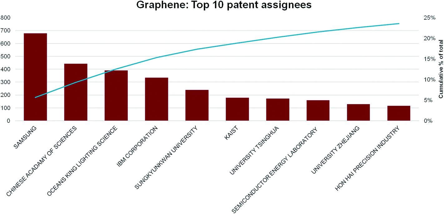
The importance of the US, China and South Korea is emphasised by the top assignees, shown in Fig. 14. The corporation with most graphene patent applications is the Korean multinational Samsung, with over three times as many filings as its nearest rival. It has also patented an unrivalled range of graphene-technology applications, including synthesis procedures,77 transparent display devices,78 composite materials,79 transistors,80 batteries and solar cells.81 Samsung’s patent applications indicate a sustained and heavy investment in graphene R&D, as well as collaboration (co-assignment of patents) with a wide range of academic institutions.82,83
Fig. 14 Top 10 graphene patent assignees by number and cumulative over all time as of end-July 2014. Number of patents are indicated in the red histograms referred to the left Y axis, while the cumulative percentage is the blue line, referred to the right Y axis.
It is also interesting to note that patent filings by universities and research institutions make up a significant proportion (50%) of total patent filings: the other half comprises contributions from small and medium-sized enterprises (SMEs) and multinationals.
Europe’s position is shown in Fig. 10, 12 and 14. While Europe makes a good showing in the geographical distribution of publications, it lags behind in patent applications, with only 7% of patent filings as compared to 30% in the US, 25% in China, and 13% in South Korea (Fig. 13) and only 9% of filings by academic institutions assigned in Europe (Fig. 15).
Fig. 15 Geographical breakdown of academic patent holders as of July 2014.
While Europe is trailing other regions in terms of number of patent filings, it nevertheless has a significant foothold in the patent landscape. Currently, the top European patent holder is Finland’s Nokia, primarily around incorporation of graphene into electrical devices, including resonators and electrodes.72,84,85
This may sound like Europe is trailing behind but that’s not the case according to the roadmap (Note: Links have been removed. Incidental numbers are footnote references),
European Universities also show promise in the graphene patent landscape. We also find evidence of corporate-academic collaborations in Europe, including e.g. co-assignments filed with European research institutions and Germany’s AMO GmbH,86 and chemical giant BASF.87,88 Finally, Europe sees significant patent filings from a number of international corporate and university players including Samsung,77 Vorbeck Materials,89 Princeton University,90–92 and Rice University,93–95 perhaps reflecting the quality of the European ST base around graphene, and its importance as a market for graphene technologies.
There are a number of features in the graphene patent landscape which may lead to a risk of patent thickets96 or ‘multiple overlapping granted patents’ existing around aspects of graphene technology systems. [emphasis mine] There is a relatively high volume of patent activity around graphene, which is an early stage technology space, with applications in patent intensive industry sectors. Often patents claim carbon nano structures other than graphene in graphene patent landscapes, illustrating difficulties around defining ‘graphene’ and mapping the graphene patent landscape. Additionally, the graphene patent nomenclature is not entirely settled. Different patent examiners might grant patents over the same components which the different experts and industry players call by different names.
For anyone new to this blog, I am not a big fan of current patent regimes as they seem to be stifling rather encouraging innovation. Sadly, patents and copyright were originally developed to encourage creativity and innovation by allowing the creators to profit from their ideas. Over time a system designed to encourage innovation has devolved into one that does the opposite. (My Oct. 31, 2011 post titled Patents as weapons and obstacles, details my take on this matter.) I’m not arguing against patents and copyright but suggesting that the system be fixed or replaced with something that delivers on the original intention.
Getting back to the matter at hand, here’s a link to and a citation for the 200 pp. 2015 European Graphene roadmap,
Science and technology roadmap for graphene, related two-dimensional crystals, and hybrid systems by Andrea C. Ferrari, Francesco Bonaccorso, Vladimir Fal’ko, Konstantin S. Novoselov, Stephan Roche, Peter Bøggild, Stefano Borini, Frank H. L. Koppens, Vincenzo Palermo, Nicola Pugno, José A. Garrido, Roman Sordan, Alberto Bianco, Laura Ballerini, Maurizio Prato, Elefterios Lidorikis, Jani Kivioja, Claudio Marinelli, Tapani Ryhänen, Alberto Morpurgo, Jonathan N. Coleman, Valeria Nicolosi, Luigi Colombo, Albert Fert, Mar Garcia-Hernandez, Adrian Bachtold, Grégory F. Schneider, Francisco Guinea, Cees Dekker, Matteo Barbone, Zhipei Sun, Costas Galiotis, Alexander N. Grigorenko, Gerasimos Konstantatos, Andras Kis, Mikhail Katsnelson, Lieven Vandersypen, Annick Loiseau, Vittorio Morandi, Daniel Neumaier, Emanuele Treossi, Vittorio Pellegrini, Marco Polini, Alessandro Tredicucci, Gareth M. Williams, Byung Hee Hong, Jong-Hyun Ahn, Jong Min Kim, Herbert Zirath, Bart J. van Wees, Herre van der Zant, Luigi Occhipinti, Andrea Di Matteo, Ian A. Kinloch, Thomas Seyller, Etienne Quesnel, Xinliang Feng, Ken Teo, Nalin Rupesinghe, Pertti Hakonen, Simon R. T. Neil, Quentin Tannock, Tomas Löfwander and Jari Kinaret. Nanoscale, 2015, Advance Article DOI: 10.1039/C4NR01600A First published online 22 Sep 2014
Here’s a diagram illustrating the roadmap process,
Fig. 122 The STRs [science and technology roadmaps] follow a hierarchical structure where the strategic level in a) is connected to the more detailed roadmap shown in b). These general roadmaps are the condensed form of the topical roadmaps presented in the previous sections, and give technological targets for key applications to become commercially competitive and the forecasts for when the targets are predicted to be met. Courtesy: Researchers and the Royal Society’s journal, Nanoscale
The image here is not the best quality; the one embedded in the relevant Nanowerk news item is better.
Today (Oct. 11, 2012), I’m highlighting a second article in Nature. This time it’s a “A roadmap for graphene ” (behind a paywall) in the Oct. 11, 2012 online issue of Nature written by Nobel Prize-winner Professor Kostya Novoselov of the University of Manchester; V. I. Fal′ko Department of Physics, Lancaster University; L. Colombo, Texas Instruments Incorporated; P. R. Gellert, AstraZeneca; M. G. Schwab, BASF SE; and K. Kim, Samsung Advanced Institute of Technology.
If you can get behind the paywall, the article offers excellent insight into the state of graphene research and the state of graphene applications. The authors cover:
Challenges in Production
Chemical vapour deposition
Synthesis on SiC
Other growth methods
Graphene electronics
Flexible electronics
High-frequency transistors
Logic transistor
Photonics
Photodetectors
Optical modulator
Mode-locked laser/THz generator
Optical polarization controller
Composite materials, paints, and coating
Energy generation and storage
Graphene for sensors and metrology
Bioapplications
You can get more details about the article from the Oct. 11, 2012 news release from the University of Manchester,
The authors estimate that the first graphene touchscreen devices could be on the market within three to five years, but will only realise its full potential in flexible electronics applications.
Rollable e-paper is another application which should be available as a prototype by 2015 – graphene’s flexibility proving ideal for fold-up electronic sheets which could revolutionise electronics.
Timescales for applications vary greatly upon the quality of graphene required, the report claims. For example, the researchers estimate devices including photo-detectors, high-speed wireless communications and THz generators (for use in medical imaging and security devices) would not be available until at least 2020, while anticancer drugs and graphene as a replacement for silicon is unlikely to become a reality until around 2030.
I notice the lead authors are from the University of Manchester and Lancaster University. These UK educational institutions are part of the FET (Future and Emerging Technologies) GRAPHENE-CA flagship project, which is in competition for one of two prizes of 1B Euros for research. As I’ve noted previously in my Feb. 21, 2012 posting and many others, the UK is leading a tremendous public relations/marketing campaign on behalf of this project and the UK’s own interests. Good luck to them as I believe the announcement of which are the two winning projects from a field of six should be made in the next few months.
The current international infatuation with roadmaps sometimes reminds me of The Wizard of Oz and the Yellow Brick Road,
I always appreciate the optimism shown by the lead character, Dorothy, as she takes off for parts unknown.
The Graphene Flagship project strikes again, this time at Graphene 2012, the second international conference on graphene. Here’s more about the conference, from the March 20, 2012 news item on Azonano,
Internationally renowned speakers will present the latest trends in the field and the global Graphene technology revolution. The Graphene 2012 program includes more than 100 speakers from all over the World, presentations from both research and industry.
…
Graphene 2012 [April 10 – 13, 2012 in Brussels, Belgium] is now an established European event, attracting global participants intent on sharing, exchanging and exploring new avenues of graphene-related scientific and commercial developments. Until now, the best, among many others, represented countries are United Kingdom, Germany, Spain, Belgium, France and United States.
I checked out the programme and found this front and centre,
Graphene Flagship Session
The consortium of the Graphene Flagship Pilot Action is working to establish the “Graphene Science and Technology Roadmap” which will be presented to the European Commission and Member States to demonstrate the need for securing long term funding, coordinated through a new Graphene Alliance. The Graphene Flagship Pilot Action will take advantage of the International conference Graphene 2012 in Brussels to co-organize a specific session in order to timely deliver to the European community the results of this Roadmap.
Tentative program
a. “Graphene Flagship: working together to combine scientific excellence and technological impacts”: Jari Kinaret
b. “The Graphene Science and Technology Roadmap”: Vladimir Falko and Andrea Ferrari
c. “Korean Graphene Research and Roadmap”: Byung Hee Hong d . “Japanese Graphene Research and Roadmap”: Masataka Hasegawa e. Round Table (tentative): Luigi Colombo, Gabriel Crean, Andrea Ferrari, Albert Fert, David Guedj, Francisco Guinea, Byung Hee Hong, Jari Kinaret, Klaus von Klitzing, and Ken Teo
I have commented previously on GRAPHENE-CA or the Graphene Flagship project, most recently in my Feb. 13, 2012 posting where I discuss the European Union’s Future and Emerging Technologies (FET) funding initiatives. The GRAPHENE-CA consortium is in competition for a 1B Euro research funding prize and they (particularly the UK) have been heroic in their promotional efforts, this new Graphene Alliance being yet another example.
A flat layer of carbon atoms packed into a two-dimensional honeycomb arrangement, graphene is being touted as a miracle (it seems) material which will enable new kinds of electronic products. Recently, there have been a number of news items and articles featuring graphene research.
Here’s my roundup of the latest and greatest graphene news. I’m starting with an application that is the closest to commercialization: IBM recently announced the creation of the first graphene-based integrated circuit. From the Bob Yirka article dated June 10, 2011 on physorg.com,
Taking a giant step forward in the creation and production of graphene based integrated circuits, IBM has announced in Science, the fabrication of a graphene based integrated circuit [IC] on a single chip. The demonstration chip, known as a radio frequency “mixer” is capable of producing frequencies up to 10 GHz, and demonstrates that it is possible to overcome the adhesion problems that have stymied researchers efforts in creating graphene based IC’s that can be used in analog applications such as cell phones or more likely military communications.
The graphene circuits were started by growing a two or three layer graphene film on a silicon surface which was then heated to 1400°C. The graphene IC was then fabricated by employing top gated, dual fingered graphene FET’s (field-effect transistors) which were then integrated with inductors. The active channels were made by spin-coating the wafer with a thin polymer and then applying a layer of hydrogen silsequioxane. The channels were then carved by e-beam lithography. Next, the excess graphene was removed with an oxygen plasma laser, and then the whole works was cleaned with acetone. The result is an integrated circuit that is less than 1mm2 in total size.
Meanwhile, there’s a graphene research project in contention for a major research prize in Europe. Worth 1B Euros, the European Union’s 2011 pathfinder programme (Future and Emerging Technologies [Fet11]) in information technology) will select two from six pilot actions currently under way to be awarded a Flagship Initiative prize. From the Fet11 flagships project page,
FET Flagships are large-scale, science-driven and mission oriented initiatives that aim to achieve a visionary technological goal. The scale of ambition is over 10 years of coordinated effort, and a budget of up to one billion Euro for each Flagship. They initiatives are coordinated between national and EU programmes and present global dimensions to foster European leadership and excellence in frontier research.
To prepare the launch of the FET Flagships, 6 Pilot Actions are funded for a 12-month period starting in May 2011. In the second half of 2012 two of the Pilots will be selected and launched as full FET Flagship Initiatives in 2013.
Here’s the description of the Graphene Science and technology for ICT and beyond pilot action,
Graphene, a new substance from the world of atomic and molecular scale manipulation of matter, could be the wonder material of the 21st century. Discovering just how important this material will be for Information and Communication Technologies is the long term focus of the Flagship Initiative, simply called, GRAPHENE. This aims to explore revolutionary potentials, in terms of both conventional as well as radically new fields of Information and Communication Technologies applications.
Bringing together multiple disciplines and addressing research across a whole range of issues, from fundamental understandings of material properties to Graphene production, the Flagship will provide the platform for establishing European scientific and technological leadership in the application of Graphene to Information and Communication Technologies. The proposed research includes coverage of electronics, spintronics, photonics, plasmonics and mechanics, all based on Graphene.
[Project Team:]
Andrea Ferrari, Cambridge University, UK
Jari Kinaret, Chalmers University, Sweden
Vladimir Falko, Lancaster University, UK
Jani Kivioja, NOKIA, Finland [emphases mine]
Not so coincidentally (given one member of the team is associated with Nokia and another is associated with Cambridge University), the Nokia Research Centre jointly with Cambridge University issued a May 4, 2011 news release (I highlighted it in my May 6, 2011 posting [scroll down past the theatre project information]) about the Morph concept (a rigid, flexible, and stretchable phone/blood pressure cuff/calculator/and other electronic devices in one product) which they have been publicizing for years now. The news release concerned itself with how graphene would enable the researchers to take the Morph from idea to actuality. The webpage for the Graphene Pilot Action is here.
There’s something breathtaking when there is no guarantee of success about the willingness to invest up to 1B Euros in a project that spans 10 years. We’ll have to wait until 2013 before learning whether the graphene project will be one of the two selected as Flagship Initiatives.
I must say the timing for the 2010 Nobel Prize for Physics which went to two scientists (Andre Geim and Konstantin Novoselov) for their groundbreaking work with graphene sems interesting (featured in my Oct. 7, 2010 posting) in light of this graphene activity.
The rest of these graphene items are about research that could lay the groundwork for future commercialization.
Hui-Ming Cheng and co-workers from the Chinese Academy of Sciences’ Institute of Metal Research at Shenyang have now devised a chemical vapor deposition (CVD) method for turning graphene sheets into porous three-dimensional ‘foams’ with extremely high conductivity (“Three-dimensional flexible and conductive interconnected graphene networks grown by chemical vapour deposition” [published in Nature Materials 10, 424–428 (2011) doi:10.1038/nmat3001 Published online 10 April 2011]). By permeating this foam with a siloxane-based polymer, the researchers have produced a composite that can be twisted, stretched and bent without harming its electrical or mechanical properties.
Here’s an image from the Nature Publishing Group (NPG) of both the vapour and the bendable, twistable, stretchable composite (downloaded from the news item on Nanowerk where you can find a larger version of the image),
The ‘elastic’ conductor (image to the right) reminds me of the ‘paper’ phone which I wrote about May 8, 2011 and May 12, 2011. (It’s a project where teams from Queen’s University [in Ontario] and Arizona State University are working to create flexible screens that give you telephony, music playing and other capabilities much like the Morph concept.)
Researchers in Singapore have developed a graphene quantum dot using a C60 (a buckminster fullerene). From the June 13, 2011 news item (Graphene: from spheres to perfect dots) on Nanowerk,
An electron trapped in a space of just a few nanometers across behaves very differently to one that is free. Structures that confine electrons in all three dimensions can produce some useful optical and electronic effects. Known as quantum dots, such structures are being widely investigated for use in new types of optical and electronics technologies, but because they are so small it is difficult to fabricate quantum dots reproducibly in terms of shape and size. Researchers from the National University of Singapore (NUS) and A*STAR have now developed a technique that enables graphene quantum dots of a known size to be created repeatedly and quickly (“Transforming C60 molecules into graphene quantum dots” [published in Nature Nanotechnology 6, 247–252 (2011) doi:10.1038/nnano.2011.30 Published online 20 March 2011]).
This final bit is about a nano PacMan that allows for more precise patterning from a June 13, 2011 article written by Michael Berger,
A widely discussed method for the patterning of graphene is the channelling of graphite by metal nanoparticles in oxidizing or reducing environments (see for instance: “Nanotechnology PacMan cuts straight graphene edges”).
“All previous studies of channelling behavior have been limited by the need to perform the experiment ex situ, i.e. comparing single ‘before’ and ‘after’ images,” Peter Bøggild, an associate professor at DTU [Danish Technical University] Nanotech, explains to Nanowerk. “In these and other ex situ experiments the dynamic behavior must be inferred from the length of channels and heating time after completion of the experiment, with the rate of formation of the channel assumed to be consistent over the course of the experiment.”
In new work, reported in the June 9, 2011 advance online edition of Nano Letters (“Discrete dynamics of nanoparticle channelling in suspended graphene” [published in Nano Letters, Article ASAP, DOI: 10.1021/nl200928k, Publication Date (Web): June 9, 2011]), Bøggild and his team report the nanoscale observation of this channelling process by silver nanoparticles in an oxygen atmosphere in-situ on suspended mono- and bilayer graphene in an environmental transmission electron microscope, enabling direct concurrent observation of the process, impossible in ex-situ experiments.
Personally, I love the youtube video I’ve included here largely because it features blobs (as many of these videos do) where they’ve added music and titles (many of these videos do not) so you can better appreciate the excitement,
From the article by Michael Berger,
As a result of watching this process occur live in a transmission electron microscope, the researchers say they have seen many details that were hidden before, and video really brings the “nano pacman” behavior to life …
There’s a reason why they’re so interested in cutting graphene,
“With a deeper understanding of the fine details we hope to one day use this nanoscale channelling behavior to directly cut desired patterns out of suspended graphene sheets, with a resolution and accuracy that isn’t achievable with any other technique,” says Bøggild. “A critical advantage here is that the graphene crystal structure guides the patterning, and in our case all of the cut edges of the graphene are ‘zigzag’ edges.”
So there you have it. IBM creates the first integrated graphene-based circuit, there’s the prospect of a huge cash prize for a 10-year project on graphene so they could produce the long awaited Morph concept and other graphene-based electronics products while a number of research teams around the world continue teasing out its secrets with graphene ‘foam’ projects, graphene quantum dots, and nano PacMen who cut graphene’s zigzag edges with precision.
ETA June 16, 2011: For those interested in the business end of things, i.e. market value of graphene-based products, Cameron Chai features a report, Graphene: Technologies, Applications, and Markets, in his June 16, 2011 news item on Azonano.
![[similar]](http://www.rsc.org/images/entities/char_223c.gif) 50%) of total patent filings: the other half comprises contributions from small and medium-sized enterprises (SMEs) and multinationals.
50%) of total patent filings: the other half comprises contributions from small and medium-sized enterprises (SMEs) and multinationals.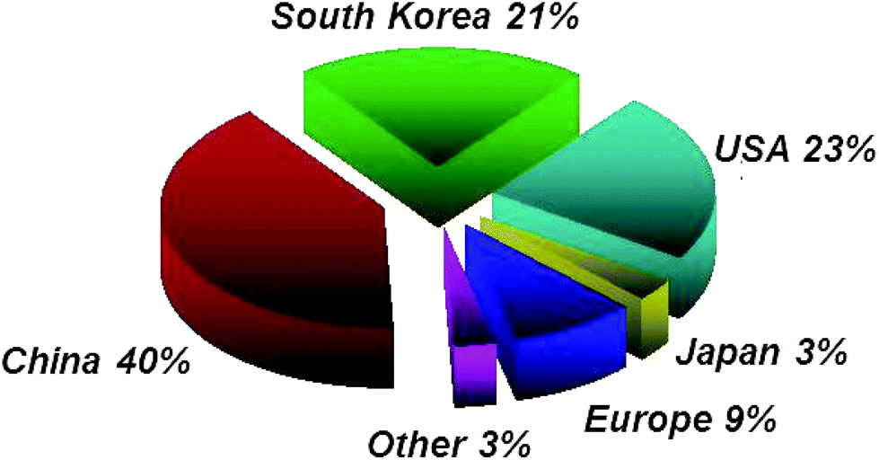
![Fig. 122 The STRs [science and technology roadmaps] follow a hierarchical structure where the strategic level in a) is connected to the more detailed roadmap shown in b). These general roadmaps are the condensed form of the topical roadmaps presented in the previous sections, and give technological targets for key applications to become commercially competitive and the forecasts for when the targets are predicted to be met. Courtesy: Researchers and the Royal Society's journal, Nanoscale](http://www.frogheart.ca/wp-content/uploads/2015/02/Euroepan-Graphene-Roadmap.gif)
