Tag Archives: wearable electronics

Making wearable technology more comfortable—with green tea for squishy supercapacitor

Researchers in India have designed a new type of wearable technology based on green team. From a Feb. 15, 2017 news item on plys.org,

Wearable electronics are here—the most prominent versions are sold in the form of watches or sports bands. But soon, more comfortable products could become available in softer materials made in part with an unexpected ingredient: green tea. Researchers report in ACS’ The Journal of Physical Chemistry C a new flexible and compact rechargeable energy storage device for wearable electronics that is infused with green tea polyphenols.

A Feb. 15, 2017 American Chemical Society (ACS) news release, (also on EurekAlert), which originated the news item, provides a little more information about the squishy supercapacitors (Note: Links have been removed),

Powering soft wearable electronics with a long-lasting source of energy remains a big challenge. Supercapacitors could potentially fill this role — they meet the power requirements, and can rapidly charge and discharge many times. But most supercapacitors are rigid, and the compressible supercapacitors developed so far have run into roadblocks. They have been made with carbon-coated polymer sponges, but the coating material tends to bunch up and compromise performance. Guruswamy Kumaraswamy, Kothandam Krishnamoorthy and colleagues wanted to take a different approach.

The researchers prepared polymer gels in green tea extract, which infuses the gel with polyphenols. The polyphenols converted a silver nitrate solution into a uniform coating of silver nanoparticles. Thin layers of conducting gold and poly(3,4-ethylenedioxythiophene) were then applied. And the resulting supercapacitor demonstrated power and energy densities of 2,715 watts per kilogram and 22 watt-hours per kilogram — enough to operate a heart rate monitor, LEDs or a Bluetooth module. The researchers tested the device’s durability and found that it performed well even after being compressed more than 100 times.

The authors acknowledge funding from the University Grants Commission of India, the Council of Scientific and Industrial Research (India) and the Board of Research in Nuclear Sciences (India).

Here’s a link to and a citation for the paper,

Elastic Compressible Energy Storage Devices from Ice Templated Polymer Gels treated with Polyphenols by Chayanika Das, Soumyajyoti Chatterjee, Guruswamy Kumaraswamy, and Kothandam Krishnamoorthy. J. Phys. Chem. C, Article ASAP DOI: 10.1021/acs.jpcc.6b12822 Publication Date (Web): January 26, 2017

Copyright © 2017 American Chemical Society

This paper is behind a paywall.

High speed fabrication of adhesive and flexible electronics

For a university that celebrated its opening in Sept. 2009 (mentioned in my Sept. 24, 2009 posting; scroll down about 40% of the way; look for a reference to the House of Wisdom), the King Abdullah University of Science and Technology (KAUST) has made some impressive announcements including this one in a Jan. 3, 2017 press release on EurekAlert,

The healthcare industry forecasts that our wellbeing in the future will be monitored by wearable wirelessly networked sensors. Manufacturing such devices could become much easier with decal electronics. A KAUST-developed process prints these high-performance silicon-based computers on to soft, sticker-like surfaces that can be attached anywhere1.

Fitting electronics on to the asymmetric contours of human bodies demands a re-think of traditional computer fabrications. One approach is to print circuit patterns on to materials such as polymers or cellulose using liquid ink made from conductive molecules. This technique enables high-speed roll-to-roll assembly of devices and packaging at low costs.

Flexible printed circuits, however, require conventional silicon components to handle applications such as digitizing analog signals. Such rigid modules can create uncomfortable hot spots on the body and increase device weight.

For the past four years, Muhammad Hussain and his team from the KAUST Computer, Electrical and Mathematical Science and Engineering Division have investigated ways to improve the flexibility of silicon materials while retaining their performance.

“We are trying to integrate all device components–sensors, data management electronics, battery, antenna–into a completely compliant system,” explained Hussain. “However, packaging these discrete modules on to soft substrates is extremely difficult.”

Searching for potential electronic skin applications, the researchers developed a sensor containing narrow strips of aluminum foil that changes conductivity at different bending states.

The devices, which could monitor a patient’s breathing patterns or activity levels, feature high-mobility zinc oxide nanotransistors on silicon wafers thinned down lithographically to microscale dimensions for maximum flexibility. Using three-dimensional (3-D) printing techniques, the team encapsulated the silicon chips and foils into a polymer film backed by an adhesive layer.

Hussain and his colleagues found a way to make the e-sticker sensors work in multiple applications. They used inkjet printing to write conductive wiring patterns on to different surfaces, such as paper or clothing. Custom-printed decals were then attached or re-adhered to each location.

“You can place a pressure-sensing decal on a tire to monitor it while driving and then peel it off and place it on your mattress to learn your sleeping patterns,” said Galo Torres Sevilla, first author of the findings and a KAUST Ph.D. graduate.

The robust performance and high-throughput manufacturing potential of decal electronics could launch a number of innovative sensor deployments, noted Hussain.

“I believe that electronics have to be democratized–simple to learn and easy to implement. Electronic decals are a right step in that direction,” Hussain said.

Here’s a link to and a citation for the paper,

Decal Electronics: Printable Packaged with 3D Printing High-Performance Flexible CMOS Electronic Systems by Galo A. Torres Sevilla, Marlon D. Cordero, Joanna M. Nassar, Amir N. Hanna, Arwa T. Kutbee, Arpys Arevalo, and Muhammad M. Hussain. Advanced Materials Technologies DOI: 10.1002/admt.201600175 Version of Record online: 13 OCT 2016

© 2016 WILEY-VCH Verlag GmbH & Co. KGaA, Weinheim

This paper is behind a paywall.

Graphene and silly putty combined to create ultra sensitive sensors

One of my favourite kinds of science story is the one where scientists turn to a children’s toy for their research. In this case, it’s silly putty. Before launching into the science part of this story, here’s more about silly putty from its Wikipedia entry (Note: A ll links have been removed),

During World War II, Japan invaded rubber-producing countries as they expanded their sphere of influence in the Pacific Rim. Rubber was vital for the production of rafts, tires, vehicle and aircraft parts, gas masks, and boots. In the U.S., all rubber products were rationed; citizens were encouraged to make their rubber products last until the end of the war and to donate spare tires, boots, and coats. Meanwhile, the government funded research into synthetic rubber compounds to attempt to solve this shortage.[10]

Credit for the invention of Silly Putty is disputed[11] and has been attributed variously to Earl Warrick,[12] of the then newly formed Dow Corning; Harvey Chin; and James Wright, a Scottish-born inventor working for General Electric in New Haven, Connecticut.[13] Throughout his life, Warrick insisted that he and his colleague, Rob Roy McGregor, received the patent for Silly Putty before Wright did; but Crayola’s history of Silly Putty states that Wright first invented it in 1943.[10][14][15] Both researchers independently discovered that reacting boric acid with silicone oil would produce a gooey, bouncy material with several unique properties. The non-toxic putty would bounce when dropped, could stretch farther than regular rubber, would not go moldy, and had a very high melting temperature. However, the substance did not have all the properties needed to replace rubber.[1]

In 1949 toy store owner Ruth Fallgatter came across the putty. She contacted marketing consultant Peter C.L. Hodgson (1912-1976).[16] The two decided to market the bouncing putty by selling it in a clear case. Although it sold well, Fallgatter did not pursue it further. However, Hodgson saw its potential.[1][3]

Already US$12,000 in debt, Hodgson borrowed US$147 to buy a batch of the putty to pack 1 oz (28 g) portions into plastic eggs for US$1, calling it Silly Putty. Initially, sales were poor, but after a New Yorker article mentioned it, Hodgson sold over 250,000 eggs of silly putty in three days.[3] However, Hodgson was almost put out of business in 1951 by the Korean War. Silicone, the main ingredient in silly putty, was put on ration, harming his business. A year later the restriction on silicone was lifted and the production of Silly Putty resumed.[17][9] Initially, it was primarily targeted towards adults. However, by 1955 the majority of its customers were aged 6 to 12. In 1957, Hodgson produced the first televised commercial for Silly Putty, which aired during the Howdy Doody Show.[18]

In 1961 Silly Putty went worldwide, becoming a hit in the Soviet Union and Europe. In 1968 it was taken into lunar orbit by the Apollo 8 astronauts.[17]

Peter Hodgson died in 1976. A year later, Binney & Smith, the makers of Crayola products, acquired the rights to Silly Putty. As of 2005, annual Silly Putty sales exceeded six million eggs.[19]

Silly Putty was inducted into the National Toy Hall of Fame on May 28, 2001. [20]

I had no idea silly putty had its origins in World War II era research. At any rate, it’s made its way back to the research lab to be united with graphene according to a Dec. 8, 2016 news item  on Nanowerk,

Researchers in AMBER, the Science Foundation Ireland-funded materials science research centre, hosted in Trinity College Dublin, have used graphene to make the novelty children’s material silly putty® (polysilicone) conduct electricity, creating extremely sensitive sensors. This world first research, led by Professor Jonathan Coleman from TCD and in collaboration with Prof Robert Young of the University of Manchester, potentially offers exciting possibilities for applications in new, inexpensive devices and diagnostics in medicine and other sectors.

A Dec. 9, 2016 Trinity College Dublin press release (also on EurekAlert), which originated the news item, describes their ‘G-putty’ in more detail,

Prof Coleman, Investigator in AMBER and Trinity’s School of Physics along with postdoctoral researcher Conor Boland, discovered that the electrical resistance of putty infused with graphene (“G-putty”) was extremely sensitive to the slightest deformation or impact. They mounted the G-putty onto the chest and neck of human subjects and used it to measure breathing, pulse and even blood pressure. It showed unprecedented sensitivity as a sensor for strain and pressure, hundreds of times more sensitive than normal sensors. The G-putty also works as a very sensitive impact sensor, able to detect the footsteps of small spiders. It is believed that this material will find applications in a range of medical devices.

Prof Coleman said, “What we are excited about is the unexpected behaviour we found when we added graphene to the polymer, a cross-linked polysilicone. This material as well known as the children’s toy silly putty. It is different from familiar materials in that it flows like a viscous liquid when deformed slowly but bounces like an elastic solid when thrown against a surface. When we added the graphene to the silly putty, it caused it to conduct electricity, but in a very unusual way. The electrical resistance of the G-putty was very sensitive to deformation with the resistance increasing sharply on even the slightest strain or impact. Unusually, the resistance slowly returned close to its original value as the putty self-healed over time.”

He continued, “While a common application has been to add graphene to plastics in order to improve the electrical, mechanical, thermal or barrier properties, the resultant composites have generally performed as expected without any great surprises. The behaviour we found with G-putty has not been found in any other composite material. This unique discovery will open up major possibilities in sensor manufacturing worldwide.”

Dexter Johnson in a Dec. 14, 2016 posting on his Nanoclast blog (on the IEEE [Institute of Electrical and Electronics Engineers]) puts this research into context,

For all the talk and research that has gone into exploiting graphene’s pliant properties for use in wearable and flexible electronics, most of the polymer composites it has been mixed with to date have been on the hard and inflexible side.

It took a team of researchers in Ireland to combine graphene with the children’s toy Silly Putty to set the nanomaterial community ablaze with excitement. The combination makes a new composite that promises to make a super-sensitive strain sensor with potential medical diagnostic applications.

“Ablaze with excitement,” eh? As Dexter rarely slips into hyperbole, this must be a big deal.

The researchers have made this video available,

For the very interested, here’s a link to and a citation for the paper,

Sensitive electromechanical sensors using viscoelastic graphene-polymer nanocomposites by Conor S. Boland, Umar Khan, Gavin Ryan, Sebastian Barwich, Romina Charifou, Andrew Harvey, Claudia Backes, Zheling Li, Mauro S. Ferreira, Matthias E. Möbius, Robert J. Young, Jonathan N. Coleman. Science  09 Dec 2016: Vol. 354, Issue 6317, pp. 1257-1260 DOI: 10.1126/science.aag2879

This paper is behind a paywall.

Self-healing lithium-ion batteries for textiles

It’s easy to forget how hard we are on our textiles. We rip them, step on them, agitate them in water, splatter them with mud, and more. So, what happens when we integrate batteries and electronics into them? An Oct. 20, 2016 news item on phys.org describes one of the latest ‘textile batter technologies’,

Electronics that can be embedded in clothing are a growing trend. However, power sources remain a problem. In the journal Angewandte Chemie, scientists have now introduced thin, flexible, lithium ion batteries with self-healing properties that can be safely worn on the body. Even after completely breaking apart, the battery can grow back together without significant impact on its electrochemical properties.

wiley_selfhealinglithiumionbattery

© Wiley-VCH

An Oct. 20, 2016 Wiley Angewandte Chemie International Edition press release (also on EurekAlert), which originated the news item, describes some of the problems associated with lithium-ion batteries and this new technology designed to address them,

Existing lithium ion batteries for wearable electronics can be bent and rolled up without any problems, but can break when they are twisted too far or accidentally stepped on—which can happen often when being worn. This damage not only causes the battery to fail, it can also cause a safety problem: Flammable, toxic, or corrosive gases or liquids may leak out.

A team led by Yonggang Wang and Huisheng Peng has now developed a new family of lithium ion batteries that can overcome such accidents thanks to their amazing self-healing powers. In order for a complicated object like a battery to be made self-healing, all of its individual components must also be self-healing. The scientists from Fudan University (Shanghai, China), the Samsung Advanced Institute of Technology (South Korea), and the Samsung R&D Institute China, have now been able to accomplish this.

The electrodes in these batteries consist of layers of parallel carbon nanotubes. Between the layers, the scientists embedded the necessary lithium compounds in nanoparticle form (LiMn2O4 for one electrode, LiTi2(PO4)3 for the other). In contrast to conventional lithium ion batteries, the lithium compounds cannot leak out of the electrodes, either while in use or after a break. The thin layer electrodes are each fixed on a substrate of self-healing polymer. Between the electrodes is a novel, solvent-free electrolyte made from a cellulose-based gel with an aqueous lithium sulfate solution embedded in it. This gel electrolyte also serves as a separation layer between the electrodes.

After a break, it is only necessary to press the broken ends together for a few seconds for them to grow back together. Both the self-healing polymer and the carbon nanotubes “stick” back together perfectly. The parallel arrangement of the nanotubes allows them to come together much better than layers of disordered carbon nanotubes. The electrolyte also poses no problems. Whereas conventional electrolytes decompose immediately upon exposure to air, the new gel is stable. Free of organic solvents, it is neither flammable nor toxic, making it safe for this application.

The capacity and charging/discharging properties of a battery “armband” placed around a doll’s elbow were maintained, even after repeated break/self-healing cycles.

Here’s a link to and a citation for the paper,

A Self-Healing Aqueous Lithium-Ion Battery by Yang Zhao, Ye Zhang, Hao Sun, Xiaoli Dong, Jingyu Cao, Lie Wang, Yifan Xu, Jing Ren, Yunil Hwang, Dr. In Hyuk Son, Dr. Xianliang Huang, Prof. Yonggang Wang, and Prof. Huisheng Peng. Angewandte Chemie International Edition DOI: 10.1002/anie.201607951 Version of Record online: 12 OCT 2016

© 2016 Wiley-VCH Verlag GmbH & Co. KGaA, Weinheim

This paper is behind a paywall.

Carrying a solar cell on a pencil or glass slide?

Caption: Ultra-thin solar cells are flexible enough to bend around small objects, such as the 1mm-thick edge of a glass slide, as shown here. Credit: Juho Kim, et al/ APL

Caption: Ultra-thin solar cells are flexible enough to bend around small objects, such as the 1mm-thick edge of a glass slide, as shown here. Credit: Juho Kim, et al/ APL

Yes, this is another wearable electronics story and this time, it’s from South Korea. A June 20, 2016 news item on ScienceDaily announces remarkably thin and flexible photovoltaics,

Scientists in South Korea have made ultra-thin photovoltaics flexible enough to wrap around the average pencil. The bendy solar cells could power wearable electronics like fitness trackers and smart glasses. …

A June 20, 2016 American Institute of Physics news release on EurekAlert, which originated the news item, expands on the theme,

Thin materials flex more easily than thick ones – think a piece of paper versus a cardboard shipping box. The reason for the difference: The stress in a material while it’s being bent increases farther out from the central plane. Because thick sheets have more material farther out they are harder to bend.

“Our photovoltaic is about 1 micrometer thick,” said Jongho Lee, an engineer at the Gwangju Institute of Science and Technology in South Korea. One micrometer is much thinner than an average human hair. Standard photovoltaics are usually hundreds of times thicker, and even most other thin photovoltaics are 2 to 4 times thicker.

The researchers made the ultra-thin solar cells from the semiconductor gallium arsenide. They stamped the cells directly onto a flexible substrate without using an adhesive that would add to the material’s thickness. The cells were then “cold welded” to the electrode on the substrate by applying pressure at 170 degrees Celcius and melting a top layer of material called photoresist that acted as a temporary adhesive. The photoresist was later peeled away, leaving the direct metal to metal bond.

The metal bottom layer also served as a reflector to direct stray photons back to the solar cells. The researchers tested the efficiency of the device at converting sunlight to electricity and found that it was comparable to similar thicker photovoltaics. They performed bending tests and found the cells could wrap around a radius as small as 1.4 millimeters.

The team also performed numerical analysis of the cells, finding that they experience one-fourth the amount of strain of similar cells that are 3.5 micrometers thick.

“The thinner cells are less fragile under bending, but perform similarly or even slightly better,” Lee said.

A few other groups have reported solar cells with thicknesses of around 1 micrometer, but have produced the cells in different ways, for example by removing the whole substract by etching.

By transfer printing instead of etching, the new method developed by Lee and his colleagues may be used to make very flexible photovoltaics with a smaller amount of materials.

The thin cells can be integrated onto glasses frames or fabric and might power the next wave of wearable electronics, Lee said.

Here’s a link to and a citation for the paper,

Ultra-thin flexible GaAs photovoltaics in vertical forms printed on metal surfaces without interlayer adhesives by Juho Kim, Jeongwoo Hwang, Kwangsun Song, Namyun Kim, Jae Cheol Shin, and Jongho Lee. Appl. Phys. Lett. 108, 253101 (2016); http://dx.doi.org/10.1063/1.4954039

This paper is open access.

Printing in midair

Dexter Johnson’s May 16, 2016 posting on his Nanoclast blog (on the IEEE [Institute of Electrical and Electronics Engineers] website) was my first introduction to something wonder-inducing (Note: Links have been removed),

While the growth of 3-D printing has led us to believe we can produce just about any structure with it, the truth is that it still falls somewhat short.

Researchers at Harvard University are looking to realize a more complete range of capabilities for 3-D printing in fabricating both planar and freestanding 3-D structures and do it relatively quickly and on low-cost plastic substrates.

In research published in the journal Proceedings of the National Academy of Sciences (PNAS),  the researchers extruded a silver-nanoparticle ink and annealed it with a laser so quickly that the system let them easily “write” free-standing 3-D structures.

While this may sound humdrum, what really takes one’s breath away with this technique is that it can create 3-D structures seemingly suspended in air without any signs of support as though they were drawn there with a pen.

Laser-assisted direct ink writing allowed this delicate 3D butterfly to be printed without any auxiliary support structure (Image courtesy of the Lewis Lab/Harvard University)

Laser-assisted direct ink writing allowed this delicate 3D butterfly to be printed without any auxiliary support structure (Image courtesy of the Lewis Lab/Harvard University)

A May 16, 2016 Harvard University press release (also on EurekAlert) provides more detail about the work,

“Flat” and “rigid” are terms typically used to describe electronic devices. But the increasing demand for flexible, wearable electronics, sensors, antennas and biomedical devices has led a team at Harvard’s John A. Paulson School of Engineering and Applied Sciences (SEAS) and Wyss Institute for Biologically Inspired Engineering to innovate an eye-popping new way of printing complex metallic architectures – as though they are seemingly suspended in midair.

“I am truly excited by this latest advance from our lab, which allows one to 3D print and anneal flexible metal electrodes and complex architectures ‘on-the-fly,’ ” said Lewis [Jennifer Lewis, the Hansjörg Wyss Professor of Biologically Inspired Engineering at SEAS and Wyss Core Faculty member].

Lewis’ team used an ink composed of silver nanoparticles, sending it through a printing nozzle and then annealing it using a precisely programmed laser that applies just the right amount of energy to drive the ink’s solidification. The printing nozzle moves along x, y, and z axes and is combined with a rotary print stage to enable freeform curvature. In this way, tiny hemispherical shapes, spiral motifs, even a butterfly made of silver wires less than the width of a hair can be printed in free space within seconds. The printed wires exhibit excellent electrical conductivity, almost matching that of bulk silver.

When compared to conventional 3D printing techniques used to fabricate conductive metallic features, laser-assisted direct ink writing is not only superior in its ability to produce curvilinear, complex wire patterns in one step, but also in the sense that localized laser heating enables electrically conductive silver wires to be printed directly on low-cost plastic substrates.

According to the study’s first author, Wyss Institute Postdoctoral Fellow Mark Skylar-Scott, Ph.D., the most challenging aspect of honing the technique was optimizing the nozzle-to-laser separation distance.

“If the laser gets too close to the nozzle during printing, heat is conducted upstream which clogs the nozzle with solidified ink,” said Skylar-Scott. “To address this, we devised a heat transfer model to account for temperature distribution along a given silver wire pattern, allowing us to modulate the printing speed and distance between the nozzle and laser to elegantly control the laser annealing process ‘on the fly.’ ”

The result is that the method can produce not only sweeping curves and spirals but also sharp angular turns and directional changes written into thin air with silver inks, opening up near limitless new potential applications in electronic and biomedical devices that rely on customized metallic architectures.

Seeing is believing, eh?

Here’s a link to and a citation for the paper,

Laser-assisted direct ink writing of planar and 3D metal architectures by Mark A. Skylar-Scott, Suman Gunasekaran, and Jennifer A. Lewis. PNAS [Proceedings of the National Academy of Sciences] 2016 doi: 10.1073/pnas.1525131113

I believe this paper is open access.

A question: I wonder what conditions are necessary before you can 3D print something in midair? Much as I’m dying to try this at home, I’m pretty that’s not possible.

Embroidering electronics into clothing

Researchers at The Ohio State University are developing embroidered antennas and circuits with 0.1 mm precision—the perfect size to integrate electronic components such as sensors and computer memory devices into clothing. Photo by Jo McCulty, courtesy of The Ohio State University.

Researchers at The Ohio State University are developing embroidered antennas and circuits with 0.1 mm precision—the perfect size to integrate electronic components such as sensors and computer memory devices into clothing. Photo by Jo McCulty, courtesy of The Ohio State University.

An April 13, 2016 news item on Nanowerk describes an advance in the field of wearable electronics,

Researchers who are working to develop wearable electronics have reached a milestone: They are able to embroider circuits into fabric with 0.1 mm precision—the perfect size to integrate electronic components such as sensors and computer memory devices into clothing.

With this advance, the Ohio State University researchers have taken the next step toward the design of functional textiles—clothes that gather, store, or transmit digital information. With further development, the technology could lead to shirts that act as antennas for your smart phone or tablet, workout clothes that monitor your fitness level, sports equipment that monitors athletes’ performance, a bandage that tells your doctor how well the tissue beneath it is healing—or even a flexible fabric cap that senses activity in the brain.

That last item is one that John Volakis, director of the ElectroScience Laboratory at Ohio State, and research scientist Asimina Kiourti are investigating. The idea is to make brain implants, which are under development to treat conditions from epilepsy to addiction, more comfortable by eliminating the need for external wiring on the patient’s body.

An April 13, 2016 Ohio State University news release by Pam Frost Gorder, which originated the news item, expands on the theme (Note: Links have been removed),

“A revolution is happening in the textile industry,” said Volakis, who is also the Roy & Lois Chope Chair Professor of Electrical Engineering at Ohio State. “We believe that functional textiles are an enabling technology for communications and sensing—and one day even medical applications like imaging and health monitoring.”

Recently, he and Kiourti refined their patented fabrication method to create prototype wearables at a fraction of the cost and in half the time as they could only two years ago. With new patents pending, they published the new results in the journal IEEE Antennas and Wireless Propagation Letters.

In Volakis’ lab, the functional textiles, also called “e-textiles,” are created in part on a typical tabletop sewing machine—the kind that fabric artisans and hobbyists might have at home. Like other modern sewing machines, it embroiders thread into fabric automatically based on a pattern loaded via a computer file. The researchers substitute the thread with fine silver metal wires that, once embroidered, feel the same as traditional thread to the touch.

“We started with a technology that is very well known—machine embroidery—and we asked, how can we functionalize embroidered shapes? How do we make them transmit signals at useful frequencies, like for cell phones or health sensors?” Volakis said. “Now, for the first time, we’ve achieved the accuracy of printed metal circuit boards, so our new goal is to take advantage of the precision to incorporate receivers and other electronic components.”

The shape of the embroidery determines the frequency of operation of the antenna or circuit, explained Kiourti.

The shape of one broadband antenna, for instance, consists of more than half a dozen interlocking geometric shapes, each a little bigger than a fingernail, that form an intricate circle a few inches across. Each piece of the circle transmits energy at a different frequency, so that they cover a broad spectrum of energies when working together—hence the “broadband” capability of the antenna for cell phone and internet access.

“Shape determines function,” she said. “And you never really know what shape you will need from one application to the next. So we wanted to have a technology that could embroider any shape for any application.”

The researchers’ initial goal, Kiourti added, was just to increase the precision of the embroidery as much as possible, which necessitated working with fine silver wire. But that created a problem, in that fine wires couldn’t provide as much surface conductivity as thick wires. So they had to find a way to work the fine thread into embroidery densities and shapes that would boost the surface conductivity and, thus, the antenna/sensor performance.

Previously, the researchers had used silver-coated polymer thread with a 0.5-mm diameter, each thread made up of 600 even finer filaments twisted together. The new threads have a 0.1-mm diameter, made with only seven filaments. Each filament is copper at the center, enameled with pure silver.

They purchase the wire by the spool at a cost of 3 cents per foot; Kiourti estimated that embroidering a single broadband antenna like the one mentioned above consumes about 10 feet of thread, for a material cost of around 30 cents per antenna. That’s 24 times less expensive than when Volakis and Kiourti created similar antennas in 2014.

In part, the cost savings comes from using less thread per embroidery. The researchers previously had to stack the thicker thread in two layers, one on top of the other, to make the antenna carry a strong enough electrical signal. But by refining the technique that she and Volakis developed, Kiourti was able to create the new, high-precision antennas in only one embroidered layer of the finer thread. So now the process takes half the time: only about 15 minutes for the broadband antenna mentioned above.

She’s also incorporated some techniques common to microelectronics manufacturing to add parts to embroidered antennas and circuits.

One prototype antenna looks like a spiral and can be embroidered into clothing to improve cell phone signal reception. Another prototype, a stretchable antenna with an integrated RFID (radio-frequency identification) chip embedded in rubber, takes the applications for the technology beyond clothing. (The latter object was part of a study done for a tire manufacturer.)

Yet another circuit resembles the Ohio State Block “O” logo, with non-conductive scarlet and gray thread embroidered among the silver wires “to demonstrate that e-textiles can be both decorative and functional,” Kiourti said.

They may be decorative, but the embroidered antennas and circuits actually work. Tests showed that an embroidered spiral antenna measuring approximately six inches across transmitted signals at frequencies of 1 to 5 GHz with near-perfect efficiency. The performance suggests that the spiral would be well-suited to broadband internet and cellular communication.

In other words, the shirt on your back could help boost the reception of the smart phone or tablet that you’re holding – or send signals to your devices with health or athletic performance data.

The work fits well with Ohio State’s role as a founding partner of the Advanced Functional Fabrics of America Institute, a national manufacturing resource center for industry and government. The new institute, which joins some 50 universities and industrial partners, was announced earlier this month by U.S. Secretary of Defense Ashton Carter.

Syscom Advanced Materials in Columbus provided the threads used in Volakis and Kiourti’s initial work. The finer threads used in this study were purchased from Swiss manufacturer Elektrisola. The research is funded by the National Science Foundation, and Ohio State will license the technology for further development.

Until then, Volakis is making out a shopping list for the next phase of the project.

“We want a bigger sewing machine,” he said.

Here’s a link to and a citation for the paper,

Fabrication of Textile Antennas and Circuits With 0.1 mm Precision by A. Kiourti, C. Lee, and J. L. Volakis.  IEEE Antennas and Wireless Propagation Letters (Volume:15 ) Page(s): 151 – 153 ISSN : 1536-1225 INSPEC Accession Number: 15785288 DOI: 10.1109/LAWP.2015.2435257 Date of Publication: 20 May 2015 Issue Date: 2016

This paper is behind a paywall.

King Abdullah University of Science and Technology (Saudi Arabia) develops sensors from household materials

Researchers at the King Adbullah University of Science and Technology (KAUST) are developing sensors made of household materials according to a Feb. 19, 2016 KAUST news release (also on EurekAlert but dated Feb. 21, 2016),

Everyday materials from the kitchen drawer, such as aluminum foil, sticky note paper, sponges and tape, have been used by a team of electrical engineers from KAUST to develop a low-cost sensor that can detect external stimuli, including touch, pressure, temperature, acidity and humidity.

The sensor, which is called Paper Skin, performs as well as other artificial skin applications currently being developed while integrating multiple functions using cost-effective materials1.

“This work has the potential to revolutionize the electronics industry and opens the door to commercializing affordable high-performance sensing devices,” stated Muhammad Mustafa Hussain from the University’s Integrated Nanotechnology Lab, where the research was conducted.

Wearable and flexible electronics show promise for a variety of applications, such as wireless monitoring of patient health and touch-free computer interfaces. Current research in this direction employs expensive and sophisticated materials and processes.

The team used sticky note paper to detect humidity, sponges and wipes to detect pressure and aluminum foil to detect motion. Coloring a sticky note with an HB pencil allowed the paper to detect acidity levels, and aluminum foil and conductive silver ink were used to detect temperature differences.

The materials were put together into a simple paper-based platform that was then connected to a device that detected changes in electrical conductivity according to external stimuli.

Increasing levels of humidity, for example, increased the platform’s ability to store an electrical charge, or its capacitance. Exposing the sensor to an acidic solution increased its resistance, while exposing it to an alkaline solution decreased it. Voltage changes were detected with temperature changes. Bringing a finger closer to the platform disturbed its electromagnetic field, decreasing its capacitance.

The team leveraged the various properties of the materials they used, including their porosity, adsorption, elasticity and dimensions to develop the low-cost sensory platform. They also demonstrated that a single integrated platform could simultaneously detect multiple stimuli in real time.

Several challenges must be overcome before a fully autonomous, flexible and multifunctional sensory platform becomes commercially achievable, explained Hussain. Wireless interaction with the paper skin needs to be developed. Reliability tests also need to be conducted to assess how long the sensor can last and how good its performance is under severe bending conditions.

“The next stage will be to optimize the sensor’s integration on this platform for applications in medical monitoring systems. The flexible and conformal sensory platform will enable simultaneous real-time monitoring of body vital signs, such as heart rate, blood pressure, breathing patterns and movement,” Hussain said.

Here’s a link to and a citation for the paper,

Paper Skin Multisensory Platform for Simultaneous Environmental Monitoring by Joanna M. Nassar, Marlon D. Cordero, Arwa T. Kutbee, Muhammad A. Karimi, Galo A. Torres Sevilla, Aftab M. Hussain, Atif Shamim, and Muhammad M. Hussain. Advanced Materials Technologies DOI: 10.1002/admt.201600004 Article first published online: 19 FEB 2016

© 2016 WILEY-VCH Verlag GmbH & Co. KGaA, Weinheim

This appears to be an open access paper.

L’Oréal introduces wearable cosmetic electronic patch (my UV patch)

You don’t (well, I don’t) expect a cosmetics company such as L’Oréal to introduce products at the Consumer Electronics Show (CES) held in Las Vegas (Nevada, US) annually (Jan. 6 – 9, 2016).

A Jan. 6, 2016 article by Zoe Kleinman for BBC (British Broadcasting Corporation) news online explains,

Beauty giant L’Oreal has unveiled a smart skin patch that can track the skin’s exposure to harmful UV rays at the technology show CES in Las Vegas.

The product will be launched in 16 countries including the UK this summer, and will be available for free [emphasis mine].

It contains a photosensitive blue dye, which changes colour when exposed to ultraviolet light.

But the wearer must take a photo of it and then upload it to an app to see the results.

It’s a free app, eh? A cynic might suggest that the company will be getting free data in return.

A Jan. 6, 2016 L’Oréal press release, also on PR Newswire, provides more details (Note: Links have been removed),

Today [Jan. 6, 2016] at the Consumer Electronics Show, L’Oréal unveiled My UV Patch, the first-ever stretchable skin sensor designed to monitor UV exposure and help consumers educate themselves about sun protection. The new technology arrives at a time when sun exposure has become a major health issue, with 90% of nonmelanoma skin cancers being associated with exposure to ultraviolet (UV) radiation from sun* in addition to attributing to skin pigmentation and photoaging.

To address these growing concerns, L’Oréal Group’s leading dermatological skincare brand, La Roche-Posay, is introducing a first-of-its kind stretchable electronic, My UV Patch. The patch is a transparent adhesive that, unlike the rigid wearables currently on the market, stretches and adheres directly to any area of skin that consumers want to monitor. Measuring approximately one square inch in area and 50 micrometers thick – half the thickness of an average strand of hair – the patch contains photosensitive dyes that factor in the baseline skin tone and change colors when exposed to UV rays to indicate varying levels of sun exposure.

Consumers will be able to take a photo of the patch and upload it to the La Roche-Posay My UV Patch mobile app, which analyzes the varying photosensitive dye squares to determine the amount of UV exposure the wearer has received. The My UV Patch mobile app will be available on both iOS and Android, incorporating Near Field Communications (NFC)-enabled technology into the patch-scanning process for Android. My UV Patch is expected to be made available to consumers later this year.

“Connected technologies have the potential to completely disrupt how we monitor the skin’s exposure to various external factors, including UV,” says Guive Balooch, Global Vice President of L’Oréal’s Technology Incubator. “Previous technologies could only tell users the amount of potential sun exposure they were receiving per hour while wearing a rigid, non-stretchable device. The key was to design a sensor that was thin, comfortable and virtually weightless so people would actually want to wear it. We’re excited to be the first beauty company entering the stretchable electronics field and to explore the many potential applications for this technology within our industry and beyond.”

My UV Patch was developed by L’Oréal’s U.S.-based Technology Incubator, a business division dedicated entirely to technological innovation, alongside MC10, Inc., a leading stretchable electronics company using cutting-edge innovation to create the most intelligent, stretchable systems for biometric healthcare analytics. L’Oréal also worked with PCH who design engineered the sensor. The stretchable, peel-and-stick wearable unites L’Oréal Group’s extensive scientific research on the skin and expertise with UV protection with MC10’s strong technological capabilities in physiological sensing and pattern recognition algorithms to measure skin changes over time, and PCH’s 20-year experience in product development, manufacturing and supply chain.

“With My UV Patch, L’Oréal is taking the lead in developing the next generation of smart skincare technology powered by MC10’s unique, stretchable electronics platform, that truly addresses a consumer need,” said Scott Pomerantz, CEO of MC10. “This partnership with L’Oréal marks an exciting new milestone for MC10 and underscores the intersection of tech and beauty and the boundless potential of connected devices within the beauty market.”

*Source: Skin Cancer Foundation 2015

“Together with La Roche-Posay dermatologists like myself, we share a mission to help increase sun safe behavior,” added Alysa Herman, MD.  “La Roche-Posay recently commissioned a global study in 23 countries, which surveyed 19,000 women and men and found a huge gap in consumer behavior: even though 92% were aware that unprotected sun exposure can cause health problems, only 26% of Americans protect themselves all year round, whatever the season. With the new My UV Patch, for the first time, we are leveraging technology to help incite a true behavioral change through real-time knowledge. ”

About L’Oréal

L’Oréal has devoted itself to beauty for over 105 years. With its unique international portfolio of 32 diverse and complementary brands, the Group generated sales amounting to 22.5 billion euros in 2014 and employs 78,600 people worldwide. As the world’s leading beauty company, L’Oréal is present across all distribution networks: mass market, department stores, pharmacies and drugstores, hair salons, travel retail and branded retail.

Research and innovation, and a dedicated research team of 3,700 people, are at the core of L’Oréal’s strategy, working to meet beauty aspirations all over the world and attract one billion new consumers in the years to come. L’Oréal’s new sustainability commitment for 2020 “Sharing Beauty With All” sets out ambitious sustainable development objectives across the Group’s value chain. www.loreal.com

About LA ROCHE-POSAY and ANTHELIOS

Recommended by more than 25,000 dermatologists worldwide, La Roche-Posay offers a unique range of daily skincare developed with dermatologists to meet their standards in efficacy, tolerance and elegant textures for increased compliance. The products, which are developed using a strict formulation charter, include a minimal number of ingredients to reduce side effects and reactivity and are formulated with effective ingredients at optimal concentrations for increased efficacy. Additionally, La Roche-Posay products undergo stringent clinical testing to guarantee efficacy and safety, even on sensitive skin.

About MC10

MC10’s mission is to improve human health through digital healthcare solutions. The company combines its proprietary ultra-thin, stretchable body-worn sensors with advanced analytics to unlock health insights from physiological data. MC10 partners with healthcare organizations and researchers to advance medical knowledge and create monitoring and diagnostic solutions for patients and physicians. Backed by a strong syndicate of financial and strategic investors, MC10 has received widespread recognition for its innovative technology, including being named a 2014 CES Innovation in Design Honoree. MC10 is headquartered in Lexington, MA.  Visit MC10 online at www.mc10inc.com.

About PCH

PCH designs custom product solutions for startups and Fortune 500 companies. Whether design engineering and development, manufacturing and fulfilment, distribution or retail, PCH takes on the toughest challenges. If it can be imagined, it can be made. At PCH, we make. www.pchintl.com. Twitter: @PCH_Intl

Ryan O’Hare’s Jan. 6, 2016 article for the UK’s DailyMailOnline provides some additional technology details and offers images of the proposed patch, not reproduced here, (Note: A link has been removed),

The patch and free app, which will be launched in the summer, have been welcomed by experts.

Dr Christopher Rowland Payne, consultant dermatologist to The London Clinic, said: ‘This is an exciting device that will motivate people in a positive way to take control of their sun exposure and will encourage them to know when it is time to leave the sun or to reapply their sunscreen.

‘It is an ingenious way of giving people the information they need. I hope it will also get people talking to each other about safe sun exposure.’

The technology used in the UV patches is based on ‘biostamps’ designed by tech firm MC10.

They were originally designed to help medical teams measure the health of their patients either remotely, or without the need for large expensive machinery.

Motorola were exploring the patches as an alternative to using traditional passwords for security and access to devices.

Getting back to this ‘free app’ business, the data gathered could be used to help the company create future skincare products. If they are planning to harvest your data, there’s nothing inherently wrong with the practice but the company isn’t being as straightforward as it could be. In any event, you may want to take a good at the user agreement and decide for yourself.

Finally, I think it’s time to acknowledge medical writer, Dr. Susan Baxter, (not for the first time and not the last either) as I likely wouldn’t have thought past my general cynicism about data harvesting for a reason, additional to any humanitarian motivations L’Oréal might have, for offering a free mobile app. She doesn’t post on her blog that frequently but it’s always worth taking a look (http://www.susanbaxter.ca/blog-page/) and I recommend this July 30, 2014 post titled, ‘Civil Scientific Discourse RIP’ which focuses on vaccination and anti-vaccination positions. Do not expect a comfortable read.

Wearable tech for Christmas 2015 and into 2016

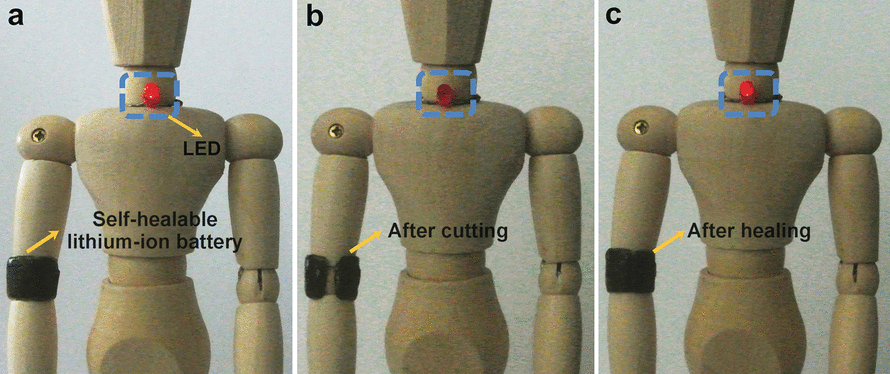
This is a roundup post of four items to cross my path this morning (Dec. 17, 2015), all of them concerned with wearable technology.

The first, a Dec. 16, 2015 news item on phys.org, is a fluffy little piece concerning the imminent arrival of a new generation of wearable technology,

It’s not every day that there’s a news story about socks. But in November [2015], a pair won the Best New Wearable Technology Device Award at a Silicon Valley conference. The smart socks, which track foot landings and cadence, are at the forefront of a new generation of wearable electronics, according to an article in Chemical & Engineering News (C&EN), the weekly newsmagazine of the American Chemical Society [ACS].

That news item was originated by a Dec. 16, 2015 ACS news release on EurekAlert which adds this,

Marc S. Reisch, a senior correspondent at C&EN, notes that stiff wristbands like the popular FitBit that measure heart rate and the number of steps people take have become common. But the long-touted technology needed to create more flexible monitoring devices has finally reached the market. Developers have successfully figured out how to incorporate stretchable wiring and conductive inks in clothing fabric, program them to transmit data wirelessly and withstand washing.

In addition to smart socks, fitness shirts and shoe insoles are on the market already or are nearly there. Although athletes are among the first to gain from the technology, the less fitness-oriented among us could also benefit. One fabric concept product — designed not for covering humans but a car steering-wheel — could sense driver alertness and make roads safer.

Reisch’s Dec. 7, 2015 article (C&EN vol. 93, issue 48, pp. 28-90) provides more detailed information and market information such as this,

Materials suppliers, component makers, and apparel developers gathered at a printed-electronics conference in Santa Clara, Calif., within a short drive of tech giants such as Google and Apple, to compare notes on embedding electronics into the routines of daily life. A notable theme was the effort to stealthily [emphasis mine] place sensors on exercise shirts, socks, and shoe soles so that athletes and fitness buffs can wirelessly track their workouts and doctors can monitor the health of their patients.

“Wearable technology is becoming more wearable,” said Raghu Das, chief executive officer of IDTechEx [emphasis mine], the consulting firm that organized the conference. By that he meant the trend is toward thinner and more flexible devices that include not just wrist-worn fitness bands but also textiles printed with stretchable wiring and electronic sensors, thanks to advances in conductive inks.

Interesting use of the word ‘stealthy’, which often suggests something sneaky as opposed to merely secretive. I imagine what’s being suggested is that the technology will not impose itself on the user (i.e., you won’t have to learn how to use it as you did with phones and computers).

Leading into my second item, IDC (International Data Corporation), not to be confused with IDTechEx, is mentioned in a Dec. 17, 2015 news item about wearable technology markets on phys.org,

The global market for wearable technology is seeing a surge, led by watches, smart clothing and other connected gadgets, a research report said Thursday [Dec. 16, 2015].

IDC said its forecast showed the worldwide wearable device market will reach a total of 111.1 million units in 2016, up 44.4 percent from this year.

By 2019, IDC sees some 214.6 million units, or a growth rate averaging 28 percent.

A Dec. 17, 2015 IDC press release, which originated the news item, provides more details about the market forecast,

“The most common type of wearables today are fairly basic, like fitness trackers, but over the next few years we expect a proliferation of form factors and device types,” said Jitesh Ubrani , Senior Research Analyst for IDC Mobile Device Trackers. “Smarter clothing, eyewear, and even hearables (ear-worn devices) are all in their early stages of mass adoption. Though at present these may not be significantly smarter than their analog counterparts, the next generation of wearables are on track to offer vastly improved experiences and perhaps even augment human abilities.”

One of the most popular types of wearables will be smartwatches, reaching a total of 34.3 million units shipped in 2016, up from the 21.3 million units expected to ship in 2015. By 2019, the final year of the forecast, total shipments will reach 88.3 million units, resulting in a five-year CAGR of 42.8%.

“In a short amount of time, smartwatches have evolved from being extensions of the smartphone to wearable computers capable of communications, notifications, applications, and numerous other functionalities,” noted Ramon Llamas , Research Manager for IDC’s Wearables team. “The smartwatch we have today will look nothing like the smartwatch we will see in the future. Cellular connectivity, health sensors, not to mention the explosive third-party application market all stand to change the game and will raise both the appeal and value of the market going forward.

“Smartwatch platforms will lead the evolution,” added Llamas. “As the brains of the smartwatch, platforms manage all the tasks and processes, not the least of which are interacting with the user, running all of the applications, and connecting with the smartphone. Once that third element is replaced with cellular connectivity, the first two elements will take on greater roles to make sense of all the data and connections.”

Top Five Smartwatch Platform Highlights

Apple’s watchOS will lead the smartwatch market throughout our forecast, with a loyal fanbase of Apple product owners and a rapidly growing application selection, including both native apps and Watch-designed apps. Very quickly, watchOS has become the measuring stick against which other smartwatches and platforms are compared. While there is much room for improvement and additional features, there is enough momentum to keep it ahead of the rest of the market.

Android/Android Wear will be a distant second behind watchOS even as its vendor list grows to include technology companies (ASUS, Huawei, LG, Motorola, and Sony) and traditional watchmakers (Fossil and Tag Heuer). The user experience on Android Wear devices has been largely the same from one device to the next, leaving little room for OEMs to develop further and users left to select solely on price and smartwatch design.

Smartwatch pioneer Pebble will cede market share to AndroidWear and watchOS but will not disappear altogether. Its simple user interface and devices make for an easy-to-understand use case, and its price point relative to other platforms makes Pebble one of the most affordable smartwatches on the market.

Samsung’s Tizen stands to be the dark horse of the smartwatch market and poses a threat to Android Wear, including compatibility with most flagship Android smartphones and an application selection rivaling Android Wear. Moreover, with Samsung, Tizen has benefited from technology developments including a QWERTY keyboard on a smartwatch screen, cellular connectivity, and new user interfaces. It’s a combination that helps Tizen stand out, but not enough to keep up with AndroidWear and watchOS.

There will be a small, but nonetheless significant market for smart wristwear running on a Real-Time Operating System (RTOS), which is capable of running third-party applications, but not on any of these listed platforms. These tend to be proprietary operating systems and OEMs will use them when they want to champion their own devices. These will help within specific markets or devices, but will not overtake the majority of the market.

The company has provided a table with five-year CAGR (compound annual growth rate) growth estimates, which can be found with the Dec. 17, 2015 IDC press release.

Disclaimer: I am not endorsing IDC’s claims regarding the market for wearable technology.

For the third and fourth items, it’s back to the science. A Dec. 17, 2015 news item on Nanowerk, describes, in general terms, some recent wearable technology research at the University of Manchester (UK), Note: A link has been removed),

Cheap, flexible, wireless graphene communication devices such as mobile phones and healthcare monitors can be directly printed into clothing and even skin, University of Manchester academics have demonstrated.

In a breakthrough paper in Scientific Reports (“Highly Flexible and Conductive Printed Graphene for Wireless Wearable Communications Applications”), the researchers show how graphene could be crucial to wearable electronic applications because it is highly-conductive and ultra-flexible.

The research could pave the way for smart, battery-free healthcare and fitness monitoring, phones, internet-ready devices and chargers to be incorporated into clothing and ‘smart skin’ applications – printed graphene sensors integrated with other 2D materials stuck onto a patient’s skin to monitor temperature, strain and moisture levels.

Detail is provided in a Dec. 17, 2015 University of Manchester press release, which originated the news item, (Note: Links have been removed),

Examples of communication devices include:

• In a hospital, a patient wears a printed graphene RFID tag on his or her arm. The tag, integrated with other 2D materials, can sense the patient’s body temperature and heartbeat and sends them back to the reader. The medical staff can monitor the patient’s conditions wirelessly, greatly simplifying the patient’s care.

• In a care home, battery-free printed graphene sensors can be printed on elderly peoples’ clothes. These sensors could detect and collect elderly people’s health conditions and send them back to the monitoring access points when they are interrogated, enabling remote healthcare and improving quality of life.

Existing materials used in wearable devices are either too expensive, such as silver nanoparticles, or not adequately conductive to have an effect, such as conductive polymers.

Graphene, the world’s thinnest, strongest and most conductive material, is perfect for the wearables market because of its broad range of superlative qualities. Graphene conductive ink can be cheaply mass produced and printed onto various materials, including clothing and paper.

“Sir Kostya Novoselov

To see evidence that cheap, scalable wearable communication devices are on the horizon is excellent news for graphene commercial applications.

Sir Kostya Novoselov (tweet)„

The researchers, led by Dr Zhirun Hu, printed graphene to construct transmission lines and antennas and experimented with these in communication devices, such as mobile and Wifi connectivity.

Using a mannequin, they attached graphene-enabled antennas on each arm. The devices were able to ‘talk’ to each other, effectively creating an on-body communications system.

The results proved that graphene enabled components have the required quality and functionality for wireless wearable devices.

Dr Hu, from the School of Electrical and Electronic Engineering, said: “This is a significant step forward – we can expect to see a truly all graphene enabled wireless wearable communications system in the near future.

“The potential applications for this research are huge – whether it be for health monitoring, mobile communications or applications attached to skin for monitoring or messaging.

“This work demonstrates that this revolutionary scientific material is bringing a real change into our daily lives.”

Co-author Sir Kostya Novoselov, who with his colleague Sir Andre Geim first isolated graphene at the University in 2004, added: “Research into graphene has thrown up significant potential applications, but to see evidence that cheap, scalable wearable communication devices are on the horizon is excellent news for graphene commercial applications.”

Here’s a link to and a citation for the paper,

Highly Flexible and Conductive Printed Graphene for Wireless Wearable Communications Applications by Xianjun Huang, Ting Leng, Mengjian Zhu, Xiao Zhang, JiaCing Chen, KuoHsin Chang, Mohammed Aqeeli, Andre K. Geim, Kostya S. Novoselov, & Zhirun Hu. Scientific Reports 5, Article number: 18298 (2015) doi:10.1038/srep18298 Published online: 17 December 2015

This is an open access paper.

The next and final item concerns supercapacitors for wearable tech, which makes it slightly different from the other items and is why, despite the date, this is the final item. The research comes from Case Western Research University (CWRU; US) according to a Dec. 16, 2015 news item on Nanowerk (Note: A link has been removed),

Wearable power sources for wearable electronics are limited by the size of garments.

With that in mind, researchers at Case Western Reserve University have developed flexible wire-shaped microsupercapacitors that can be woven into a jacket, shirt or dress (Energy Storage Materials, “Flexible and wearable wire-shaped microsupercapacitors based on highly aligned titania and carbon nanotubes”).

A Dec. 16, 2015 CWRU news release (on EurekAlert), which originated the news item, provides more detail about a device that would make wearable tech more wearable (after all, you don’t want to recharge your clothes the same way you do your phone and other mobile devices),

By their design or by connecting the capacitors in series or parallel, the devices can be tailored to match the charge storage and delivery needs of electronics donned.

While there’s been progress in development of those electronics–body cameras, smart glasses, sensors that monitor health, activity trackers and more–one challenge remaining is providing less obtrusive and cumbersome power sources.

“The area of clothing is fixed, so to generate the power density needed in a small area, we grew radially-aligned titanium oxide nanotubes on a titanium wire used as the main electrode,” said Liming Dai, the Kent Hale Smith Professor of Macromolecular Science and Engineering. “By increasing the surface area of the electrode, you increase the capacitance.”

Dai and Tao Chen, a postdoctoral fellow in molecular science and engineering at Case Western Reserve, published their research on the microsupercapacitor in the journal Energy Storage Materials this week. The study builds on earlier carbon-based supercapacitors.

A capacitor is cousin to the battery, but offers the advantage of charging and releasing energy much faster.

How it works

In this new supercapacitor, the modified titanium wire is coated with a solid electrolyte made of polyvinyl alcohol and phosphoric acid. The wire is then wrapped with either yarn or a sheet made of aligned carbon nanotubes, which serves as the second electrode. The titanium oxide nanotubes, which are semiconducting, separate the two active portions of the electrodes, preventing a short circuit.

In testing, capacitance–the capability to store charge–increased from 0.57 to 0.9 to 1.04 milliFarads per micrometer as the strands of carbon nanotube yarn were increased from 1 to 2 to 3.

When wrapped with a sheet of carbon nanotubes, which increases the effective area of electrode, the microsupercapactitor stored 1.84 milliFarads per micrometer. Energy density was 0.16 x 10⁻³ milliwatt-hours per cubic centimeter and power density .01 milliwatt per cubic centimeter.

Whether wrapped with yarn or a sheet, the microsupercapacitor retained at least 80 percent of its capacitance after 1,000 charge-discharge cycles. To match various specific power needs of wearable devices, the wire-shaped capacitors can be connected in series or parallel to raise voltage or current, the researchers say.

When bent up to 180 degrees hundreds of times, the capacitors showed no loss of performance. Those wrapped in sheets showed more mechanical strength.

“They’re very flexible, so they can be integrated into fabric or textile materials,” Dai said. “They can be a wearable, flexible power source for wearable electronics and also for self-powered biosensors or other biomedical devices, particularly for applications inside the body.” [emphasis mine]

Dai ‘s lab is in the process of weaving the wire-like capacitors into fabric and integrating them with a wearable device.

So one day we may be carrying supercapacitors in our bodies? I’m not sure how I feel about that goal. In any event, here’s a link and a citation for the paper,

Flexible and wearable wire-shaped microsupercapacitors based on highly aligned titania and carbon nanotubes by Tao Chen, Liming Dai. Energy Storage Materials Volume 2, January 2016, Pages 21–26 doi:10.1016/j.ensm.2015.11.004

This paper appears to be open access.