University of Maryland researchers are suggesting that transparent wood could be more energy efficient than glass. An Aug. 16, 2016 news item on ScienceDaily describes the research,
Engineers at the A. James Clark School of Engineering at the University of Maryland (UMD) demonstrate in a new study that windows made of transparent wood could provide more even and consistent natural lighting and better energy efficiency than glass.
An Aug. 16, 2016 University of Maryland news release (also on EurekAlert) which originated the news item, explains further,
In a paper just published in the peer-reviewed journal Advanced Energy Materials, the team, headed by Liangbing Hu of UMD’s Department of Materials Science and Engineering and the Energy Research Center lay out research showing that their transparent wood provides better thermal insulation and lets in nearly as much light as glass, while eliminating glare and providing uniform and consistent indoor lighting. The findings advance earlier published work on their development of transparent wood.
The transparent wood lets through just a little bit less light than glass, but a lot less heat, said Tian Li, the lead author of the new study. “It is very transparent, but still allows for a little bit of privacy because it is not completely see-through. We also learned that the channels in the wood transmit light with wavelengths around the range of the wavelengths of visible light, but that it blocks the wavelengths that carry mostly heat,” said Li.
The team’s findings were derived, in part, from tests on tiny model house with a transparent wood panel in the ceiling that the team built. The tests showed that the light was more evenly distributed around a space with a transparent wood roof than a glass roof.
The channels in the wood direct visible light straight through the material, but the cell structure that still remains bounces the light around just a little bit, a property called haze. This means the light does not shine directly into your eyes, making it more comfortable to look at. The team photographed the transparent wood’s cell structure in the University of Maryland’s Advanced Imaging and Microscopy (AIM) Lab.
Transparent wood still has all the cell structures that comprised the original piece of wood. The wood is cut against the grain, so that the channels that drew water and nutrients up from the roots lie along the shortest dimension of the window. The new transparent wood uses theses natural channels in wood to guide the sunlight through the wood.
As the sun passes over a house with glass windows, the angle at which light shines through the glass changes as the sun moves. With windows or panels made of transparent wood instead of glass, as the sun moves across the sky, the channels in the wood direct the sunlight in the same way every time.
“This means your cat would not have to get up out of its nice patch of sunlight every few minutes and move over,” Li said. “The sunlight would stay in the same place. Also, the room would be more equally lighted at all times.”
Working with transparent wood is similar to working with natural wood, the researchers said. However, their transparent wood is waterproof due to its polymer component. It also is much less breakable than glass because the cell structure inside resists shattering.
The research team has recently patented their process for making transparent wood. The process starts with bleaching from the wood all of the lignin, which is a component in the wood that makes it both brown and strong. The wood is then soaked in epoxy, which adds strength back in and also makes the wood clearer. The team has used tiny squares of linden wood about 2 cm x 2 cm, but the wood can be any size, the researchers said.
Here’s an image illustrating the research,
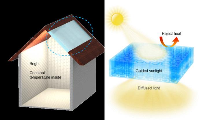
Caption: This is a wood composite as an energy efficient building material: Guided sunlight transmission and effective thermal insulation. Credit: University of Maryland and Advanced Energy Materials
I have written about transparent wood twice before. There’s this April 1, 2016 posting about the work at the KTH Institute (Sweden) and a May 11, 2016 posting about some earlier work at the University of Maryland.
Here’s a link and a citation for the latest from the University of Maryland,
Wood Composite as an Energy Efficient Building Material: Guided Sunlight Transmittance and Effective Thermal Insulation by Tian Li, Mingwei Zhu, Zhi Yang, Jianwei Song, Jiaqi Dai, Yonggang Yao, Wei Luo, Glenn Pastel, Bao Yang, and Liangbing Hu. Advanced Energy Materials Version of Record online: 11 AUG 2016
© 2016 WILEY-VCH Verlag GmbH & Co. KGaA, Weinheim
This paper is behind a paywall.