Nanodiamonds if successfully extracted from oil could be used for imaging and communications and the world’s leading program for extracting nanodiamonds (also known as diamondoids) is in California (US). From a May 12, 2016 news item on Nanowerk,
Stanford and SLAC National Accelerator Laboratory jointly run the world’s leading program for isolating and studying diamondoids — the tiniest possible specks of diamond. Found naturally in petroleum fluids, these interlocking carbon cages weigh less than a billionth of a billionth of a carat (a carat weighs about the same as 12 grains of rice); the smallest ones contain just 10 atoms.
Over the past decade, a team led by two Stanford-SLAC faculty members — Nick Melosh, an associate professor of materials science and engineering and of photon science, and Zhi-Xun Shen, a professor of photon science and of physics and applied physics – has found potential roles for diamondoids in improving electron microscope images, assembling materials and printing circuits on computer chips. The team’s work takes place within SIMES, the Stanford Institute for Materials and Energy Sciences, which is run jointly with SLAC.
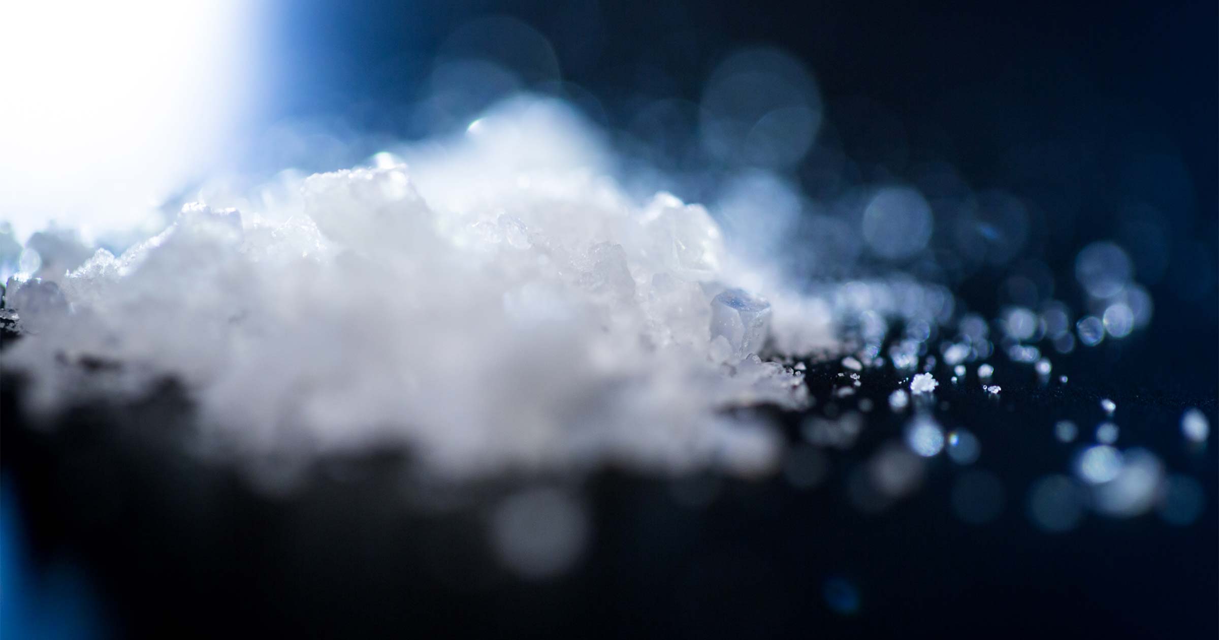
Close-up of purified diamondoids on a lab bench. Too small to see with the naked eye, diamondoids are visible only when they clump together in fine, sugar-like crystals like these. Photo: Christopher Smith, SLAC National Accelerator Laboratory
A March 31, 2016 Stanford University news release by Glennda Chui, which originated the news item, describes the work in more detail,
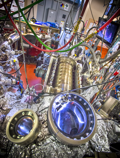
Before they can do that [use nanodiamonds in imaging and other applications], though, just getting the diamondoids is a technical feat. It starts at the nearby Chevron refinery in Richmond, California, with a railroad tank car full of crude oil from the Gulf of Mexico. “We analyzed more than a thousand oils from around the world to see which had the highest concentrations of diamondoids,” says Jeremy Dahl, who developed key diamondoid isolation techniques with fellow Chevron researcher Robert Carlson before both came to Stanford — Dahl as a physical science research associate and Carlson as a visiting scientist.
The original isolation steps were carried out at the Chevron refinery, where the selected crudes were boiled in huge pots to concentrate the diamondoids. Some of the residue from that work came to a SLAC lab, where small batches are repeatedly boiled to evaporate and isolate molecules of specific weights. These fluids are then forced at high pressure through sophisticated filtration systems to separate out diamondoids of different sizes and shapes, each of which has different properties.
The diamondoids themselves are invisible to the eye; the only reason we can see them is that they clump together in fine, sugar-like crystals. “If you had a spoonful,” Dahl says, holding a few in his palm, “you could give 100 billion of them to every person on Earth and still have some left over.”
Recently, the team started using diamondoids to seed the growth of flawless, nano-sized diamonds in a lab at Stanford. By introducing other elements, such as silicon or nickel, during the growing process, they hope to make nanodiamonds with precisely tailored flaws that can produce single photons of light for next-generation optical communications and biological imaging.
Early results show that the quality of optical materials grown from diamondoid seeds is consistently high, says Stanford’s Jelena Vuckovic, a professor of electrical engineering who is leading this part of the research with Steven Chu, professor of physics and of molecular and cellular physiology.
“Developing a reliable way of growing the nanodiamonds is critical,” says Vuckovic, who is also a member of Stanford Bio-X. “And it’s really great to have that source and the grower right here at Stanford. Our collaborators grow the material, we characterize it and we give them feedback right away. They can change whatever we want them to change.”