Category Archives: light

Reconfiguring a LEGO-like AI chip with light

MIT engineers have created a reconfigurable AI chip that comprises alternating layers of sensing and processing elements that can communicate with each other. Credit: Figure courtesy of the researchers and edited by MIT News

This image certainly challenges any ideas I have about what Lego looks like. It seems they see things differently at the Massachusetts Institute of Technology (MIT). From a June 13, 2022 MIT news release (also on EurekAlert),

Imagine a more sustainable future, where cellphones, smartwatches, and other wearable devices don’t have to be shelved or discarded for a newer model. Instead, they could be upgraded with the latest sensors and processors that would snap onto a device’s internal chip — like LEGO bricks incorporated into an existing build. Such reconfigurable chipware could keep devices up to date while reducing our electronic waste. 

Now MIT engineers have taken a step toward that modular vision with a LEGO-like design for a stackable, reconfigurable artificial intelligence chip.

The design comprises alternating layers of sensing and processing elements, along with light-emitting diodes (LED) that allow for the chip’s layers to communicate optically. Other modular chip designs employ conventional wiring to relay signals between layers. Such intricate connections are difficult if not impossible to sever and rewire, making such stackable designs not reconfigurable.

The MIT design uses light, rather than physical wires, to transmit information through the chip. The chip can therefore be reconfigured, with layers that can be swapped out or stacked on, for instance to add new sensors or updated processors.

“You can add as many computing layers and sensors as you want, such as for light, pressure, and even smell,” says MIT postdoc Jihoon Kang. “We call this a LEGO-like reconfigurable AI chip because it has unlimited expandability depending on the combination of layers.”

The researchers are eager to apply the design to edge computing devices — self-sufficient sensors and other electronics that work independently from any central or distributed resources such as supercomputers or cloud-based computing.

“As we enter the era of the internet of things based on sensor networks, demand for multifunctioning edge-computing devices will expand dramatically,” says Jeehwan Kim, associate professor of mechanical engineering at MIT. “Our proposed hardware architecture will provide high versatility of edge computing in the future.”

The team’s results are published today in Nature Electronics. In addition to Kim and Kang, MIT authors include co-first authors Chanyeol Choi, Hyunseok Kim, and Min-Kyu Song, and contributing authors Hanwool Yeon, Celesta Chang, Jun Min Suh, Jiho Shin, Kuangye Lu, Bo-In Park, Yeongin Kim, Han Eol Lee, Doyoon Lee, Subeen Pang, Sang-Hoon Bae, Hun S. Kum, and Peng Lin, along with collaborators from Harvard University, Tsinghua University, Zhejiang University, and elsewhere.

Lighting the way

The team’s design is currently configured to carry out basic image-recognition tasks. It does so via a layering of image sensors, LEDs, and processors made from artificial synapses — arrays of memory resistors, or “memristors,” that the team previously developed, which together function as a physical neural network, or “brain-on-a-chip.” Each array can be trained to process and classify signals directly on a chip, without the need for external software or an Internet connection.

In their new chip design, the researchers paired image sensors with artificial synapse arrays, each of which they trained to recognize certain letters — in this case, M, I, and T. While a conventional approach would be to relay a sensor’s signals to a processor via physical wires, the team instead fabricated an optical system between each sensor and artificial synapse array to enable communication between the layers, without requiring a physical connection. 

“Other chips are physically wired through metal, which makes them hard to rewire and redesign, so you’d need to make a new chip if you wanted to add any new function,” says MIT postdoc Hyunseok Kim. “We replaced that physical wire connection with an optical communication system, which gives us the freedom to stack and add chips the way we want.”

The team’s optical communication system consists of paired photodetectors and LEDs, each patterned with tiny pixels. Photodetectors constitute an image sensor for receiving data, and LEDs to transmit data to the next layer. As a signal (for instance an image of a letter) reaches the image sensor, the image’s light pattern encodes a certain configuration of LED pixels, which in turn stimulates another layer of photodetectors, along with an artificial synapse array, which classifies the signal based on the pattern and strength of the incoming LED light.

Stacking up

The team fabricated a single chip, with a computing core measuring about 4 square millimeters, or about the size of a piece of confetti. The chip is stacked with three image recognition “blocks,” each comprising an image sensor, optical communication layer, and artificial synapse array for classifying one of three letters, M, I, or T. They then shone a pixellated image of random letters onto the chip and measured the electrical current that each neural network array produced in response. (The larger the current, the larger the chance that the image is indeed the letter that the particular array is trained to recognize.)

The team found that the chip correctly classified clear images of each letter, but it was less able to distinguish between blurry images, for instance between I and T. However, the researchers were able to quickly swap out the chip’s processing layer for a better “denoising” processor, and found the chip then accurately identified the images.

“We showed stackability, replaceability, and the ability to insert a new function into the chip,” notes MIT postdoc Min-Kyu Song.

The researchers plan to add more sensing and processing capabilities to the chip, and they envision the applications to be boundless.

“We can add layers to a cellphone’s camera so it could recognize more complex images, or makes these into healthcare monitors that can be embedded in wearable electronic skin,” offers Choi, who along with Kim previously developed a “smart” skin for monitoring vital signs.

Another idea, he adds, is for modular chips, built into electronics, that consumers can choose to build up with the latest sensor and processor “bricks.”

“We can make a general chip platform, and each layer could be sold separately like a video game,” Jeehwan Kim says. “We could make different types of neural networks, like for image or voice recognition, and let the customer choose what they want, and add to an existing chip like a LEGO.”

This research was supported, in part, by the Ministry of Trade, Industry, and Energy (MOTIE) from South Korea; the Korea Institute of Science and Technology (KIST); and the Samsung Global Research Outreach Program.

Here’s a link to and a citation for the paper,

Reconfigurable heterogeneous integration using stackable chips with embedded artificial intelligence by Chanyeol Choi, Hyunseok Kim, Ji-Hoon Kang, Min-Kyu Song, Hanwool Yeon, Celesta S. Chang, Jun Min Suh, Jiho Shin, Kuangye Lu, Bo-In Park, Yeongin Kim, Han Eol Lee, Doyoon Lee, Jaeyong Lee, Ikbeom Jang, Subeen Pang, Kanghyun Ryu, Sang-Hoon Bae, Yifan Nie, Hyun S. Kum, Min-Chul Park, Suyoun Lee, Hyung-Jun Kim, Huaqiang Wu, Peng Lin & Jeehwan Kim. Nature Electronics volume 5, pages 386–393 (2022) 05 May 2022 Issue Date: June 2022 Published: 13 June 2022 DOI: https://doi.org/10.1038/s41928-022-00778-y

This paper is behind a paywall.
Tunable metasurfaces and reshaping the future of light

Thinner, meaning smaller and less bulky, is a prized quality in technologies such as phones, batteries, and, in this case, lenses. From a May 16, 2022 news item on ScienceDaily,

The technological advancement of optical lenses has long been a significant marker of human scientific achievement. Eyeglasses, telescopes, cameras, and microscopes have all literally and figuratively allowed us to see the world in a new light. Lenses are also a fundamental component of manufacturing nanoelectronics by the semiconductor industry.

One of the most impactful breakthroughs of lens technology in recent history has been the development of photonic metasurfaces — artificially engineered nano-scale materials with remarkable optical properties. Georgia Tech [Georgia Institute of Technology] researchers at the forefront of this technology have recently demonstrated the first-ever electrically tunable photonic metasurface platform in a recent study published by Nature Communications.

“Metasurfaces can make the optical systems very thin, and as they become easier to control and tune, you’ll soon find them in cell phone cameras and similar electronic imaging systems,” said Ali Adibi, professor in the School of Electrical and Computer Engineering at the Georgia Institute of Technology [Georgia Tech; US].

A May 10, 2022 Georgia Tech news release (also on EurekAlert but published May 16, 2022), which originated the news item, provides more detail,

The pronounced tuning measures achieved through the new platform represent a critical advancement towards the development of miniaturized reconfigurable metasurfaces. The results of the study have shown a record eleven-fold change in the reflective properties, a large range of spectral tuning for operation, and much faster tuning speed.

Heating Up Metasurfaces

Metasurfaces are a class of nanophotonic materials in which a large range of miniaturized elements are engineered to affect the transmission and reflection of light at different frequencies in a controlled way.

“When viewing under very strong microscopes, metasurfaces look like a periodic array of posts,” said Adibi. “The best analogy would be to think of a LEGO pattern formed by connecting many similar LEGO bricks next to each other.”

Since their inception, metasurfaces have been used to demonstrate that very thin optical devices can affect light propagation with metalenses (the formation of thin lenses) being the most developed application.

Despite impressive progress, most demonstrated metasurfaces are passive, meaning their performance cannot be changed (or tuned) after fabrication. The work presented by Adibi and his team, led by Ph.D. candidate Sajjad Abdollahramezani, applies electrical heat to a special class of nanophotonic materials to create a platform that can enable reconfigurable metasurfaces to be easily manufactured with high levels of optical modulation.

PCMs Provide the Answer

A wide range of materials may be used to form metasurfaces including metals, oxides, and semiconductors, but Abdollahramezani and Adibi’s research focuses on phase-change materials (PCMs) because they can form the most effective structures with the smallest feature sizes. PCMs are substances that absorb and release heat during the process of heating and cooling. They are called “phase-change” materials because they go from one crystallization state to another during the thermal cycling process. Water changing from a liquid to a solid or gas is the most common example.

The Georgia Tech team’s experiments are substantially more complicated than heating and freezing water. Knowing that the optical properties of PCMs can be altered by local heating, they have harnessed the full potential of the PCM alloy Ge2Sb2Te5 (GST), which is a compound of germanium, antimony, and tellurium.

By combining the optical design with a miniaturized electrical microheater underneath, the team can change the crystalline phase of the GST to make active tuning of the metasurface device possible. The fabricated metasurfaces were developed at Georgia Tech’s Institute for Electronics and Nanotechnology (IEN) and tested in characterization labs by illuminating the reconfigurable metasurfaces with laser light at different frequencies and measuring the properties of the reflected light in real time.

What Tunable Metasurfaces Mean for the Future

Driven by device miniaturization and system integration, as well as their ability to selectively reflect different colors of light, metasurfaces are rapidly replacing bulky optical assemblies of the past. Immediate impact on technologies like LiDAR systems for autonomous cars, imaging, spectroscopy, and sensing is expected.

With further development, more aggressive applications like computing, augmented reality, photonic chips for artificial intelligence, and biohazard detection can also be envisioned, according to Abdollahramezani and Adibi.

“As the platform continues to develop, reconfigurable metasurfaces will be found everywhere,” said Adibi. “They will even empower smaller endoscopes to go deep inside the body for better imaging and help medical sensors detect different biomarkers in blood.”

Funding: This material is based upon work supported by the National Science Foundation (NSF) under Grant No. 1837021. Any opinions, findings, and conclusions or recommendations expressed in this material are those of the authors and do not necessarily reflect the views of the NSF. The work was primarily funded by Office of Naval Research (ONR) (N00014-18-1-2055, Dr. B. Bennett) and by Defense Advanced Research Projects Agency [DARPA] (D19AC00001, Dr. R. Chandrasekar). W.C. acknowledges support from ONR (N00014-17-1-2555) and National Science Foundation (NSF) (DMR-2004749). A. Alù acknowledges support from Air Force Office of Scientific Research and the Simons Foundation. M.W. acknowledges support by the Deutsche Forschungsgemeinschaft (SFB 917). M.E.S. acknowledges financial support of NSF-CHE (1608801). This work was performed in part at the Georgia Tech Institute for Electronics and Nanotechnology (IEN), a member of the National Nanotechnology Coordinated Infrastructure (NNCI), which is supported by NSF (ECCS1542174).

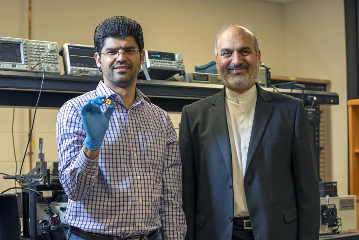
Caption: Georgia Tech professor Ali Adibi [on the right] with Ph.D. candidate Sajjad Abdollahramezani [on th eleft holding an unidentified object] in Ali’s Photonics Research Group lab where the characterization of the tunable metasurfaces takes place. Credit: Georgia Tech

I am charmed by this image. Neither of these two are professionals at posing for photographers. Nonetheless, they look pleased and happy to help the publicity team spread the word about their research, they also seem like they’re looking forward to getting back to work.

Here’s a link to and a citation for the paper,

Electrically driven reprogrammable phase-change metasurface reaching 80% efficiency by Sajjad Abdollahramezani, Omid Hemmatyar, Mohammad Taghinejad, Hossein Taghinejad, Alex Krasnok, Ali A. Eftekhar, Christian Teichrib, Sanchit Deshmukh, Mostafa A. El-Sayed, Eric Pop, Matthias Wuttig, Andrea Alù, Wenshan Cai & Ali Adibi. Nature Communications volume 13, Article number: 1696 (2022) DOI: https://doi.org/10.1038/s41467-022-29374-6 Published: 30 March 2022

This paper is open access.

The reddest red and Schrödinger’s red pixel

Caption: Schrödinger’s red pixel by quasi-bound-states in-the-continuum Credit: 123RF

Science keeps moving. First, there was the June 2022 news and, then, there was the August 2022 news.

A June 8, 2022 Agency for Science, Technology and Research (A*STAR) press release (also on EurekAlert but published June 7, 2022 as an ‘article highlight’) announces more research into structural colour along with some colour theory from Erwin Schrödinger,

The brilliant and often iridescent colours that we see in some species of birds, beetles and butterflies arise from a regular arrangement of nanostructures that scatter selective wavelengths of light more strongly to generate colour. These colours are called structural colours, which usually range from blues to greens, and even magenta. However, vibrant or saturated reds are elusive and notably absent from the structural colour range in both natural and synthetic realms.

To achieve highly saturated reds, the material needs to absorb light from all wavelengths shorter than ~600 nm and reflect the remaining longer wavelengths, doing both as completely as possible. This sharp transition from absorption to reflection was prescribed theoretically by none other than Erwin Schrödinger of quantum theory fame. However, the physics of resonators tell us that high-order optical resonances in blue will also occur as soon as we have a fundamental resonance in red. This combination of blue and red thus results in the magenta observed in nature. It is therefore challenging to achieve the Schrödinger’s red pixel, which would produce the most saturated red in the world. Current nanoantenna-based approaches are insufficient to simultaneously satisfy the above conditions.

Researchers from the Agency for Science, Technology and Research’s (A*STAR) Institute of Materials Research and Engineering (IMRE), National University of Singapore (NUS) and Singapore University of Technology and Design (SUTD) have collaborated to design and realise reds at the ultimate limit of saturation as predicted by theory, where the team worked together on conceptualisation methodology, fabrications, characterisations and simulations. This research was published in Science Advances on 23 February 2022.

The design consists of regularly arranged silicon nanoantennas in the shape of ellipses. These produce possibly the most saturated and brightest reds with ~80% reflectance, exceeding the reds in the standard red, green and blue gamut (sRGB) and other well-known red pigments, e.g. cadmium red .

The nanoantennas support two partially overlapping quasi bound-states-in-the-continuum modes, where the optimal dimensions of the silicon nanoantenna arrays are derived by using a gradient descent algorithm to enable the antennas to achieve sharp spectral edges at red wavelengths. At the same time, high-order modes at blue or green wavelengths are suppressed via engineering the substrate‑induced diffraction channels and the absorption of amorphous silicon.

Potential uses for Schrödinger’s red include developing a polarisation dependent encryption method, with plans to scale up the Schrödinger’s red pixel for applications like functional nanofabrication devices such as optical spectrometers and reflective displays with high colour saturation.

“With this new design that can achieve the most saturated and brightest reds, we can exploit its sensitivity to polarisation and illumination angle on potential applications for information encryption. This proposed concept and design methodology could also be generalised to other Schrödinger’s colour pixels. The highly-saturated red achieved could be potentially scaled up through methods such as deep ultraviolet and nano-imprint lithography, to reach the dimensions of reflective displays based on multilayer film configuration, which could lead to potential applications like compact red filters, highly saturated reflective displays, nonlocal metasurfaces, and miniaturised spectrometers”, said Dr. Dong Zhaogang, Deputy Department Head of Nanofabrication at A*STAR’s IMRE.

“The creation of the record-high saturation and brightness in red opens up possibilities for a plethora of applications related to anti-counterfeiting technologies, high-calibre colour display and more, which were previously perceived as unachievable with structural colour. It showcases a wonderful synergy between conceptual breakthrough, powerful algorithm and advanced nanofabrication”, said Prof. Cheng-Wei Qiu, Dean’s Chair Professor at NUS.

“This work in structural colours goes to show that we can sometimes outdo evolution through clever use of the tools in nanofabrication and accurate optical simulations”, said Prof. Joel Yang, Provost Chair Professor and Associate Professor in Engineering Product Development at SUTD.

Here’s a link to and a citation for the paper,

Schrödinger’s red pixel by quasi-bound-states-in-the-continuum by Zhaogang Dong, Lei Jin, Soroosh Daqiqeh Rezaei, Hao Wang, Yang Chen, Febiana Tjiptoharsono, Jinfa Ho, Sergey Gorelik, Ray Jia Hong Ng, Qifeng Ruan, Cheng-Wei Qiu and Joel K. W. Yang. Science Advances Vol 8, Issue 8 DOI: 10.1126/sciadv.abm4512 Published 23 Feb 2022

This paper is open access.

Math error, colour theory, and perception

An August 10, 2022 news item on phys.org announced a math error made by Erwin Schrödinger and others,

A new study corrects an important error in the 3D mathematical space developed by the Nobel Prize-winning physicist Erwin Schrödinger and others, and used by scientists and industry for more than 100 years to describe how your eye distinguishes one color from another. The research has the potential to boost scientific data visualizations, improve TVs and recalibrate the textile and paint industries.

“The assumed shape of color space requires a paradigm shift,” said Roxana Bujack, a computer scientist with a background in mathematics who creates scientific visualizations at Los Alamos National Laboratory. Bujack is lead author of the paper by a Los Alamos team in the Proceedings of the National Academy of Sciences on the mathematics of color perception.

“Our research shows that the current mathematical model of how the eye perceives color differences is incorrect. That model was suggested by Bernhard Riemann and developed by Hermann von Helmholtz and Erwin Schrödinger—all giants in mathematics and physics—and proving one of them wrong is pretty much the dream of a scientist,” said Bujack.

While the Los Alamos National Laboratory work was published in April 2022 (online) and May 2022 (in print), their news announcement doesn’t seem to have been made until August. I can’t be certain but I believe this should have an impact on the work from A*STAR as that team’s paper cites: E. Schrödinger, Theorie der Pigmente von größter Leuchtkraft. Ann. Phys. 367, 603–622 (1920).

An August 10, 2022 Los Alamos National Laboratory (LANL) news release (also on EurekAlert) provides more information about the discovery,

Modeling human color perception enables automation of image processing, computer graphics and visualization tasks.

“Our original idea was to develop algorithms to automatically improve color maps for data visualization, to make them easier to understand and interpret,” Bujack said. So the team was surprised when they discovered they were the first to determine that the longstanding application of Riemannian geometry, which allows generalizing straight lines to curved surfaces, didn’t work.

To create industry standards, a precise mathematical model of perceived color space is needed. First attempts used Euclidean spaces—the familiar geometry taught in many high schools; more advanced models used Riemannian geometry. The models plot red, green and blue in the 3D space. Those are the colors registered most strongly by light-detecting cones on our retinas, and—not surprisingly—the colors that blend to create all the images on your RGB computer screen.

In the study, which blends psychology, biology and mathematics, Bujack and her colleagues discovered that using Riemannian geometry overestimates the perception of large color differences. That’s because people perceive a big difference in color to be less than the sum you would get if you added up small differences in color that lie between two widely separated shades.

Riemannian geometry cannot account for this effect.

“We didn’t expect this, and we don’t know the exact geometry of this new color space yet,” Bujack said. “We might be able to think of it normally but with an added dampening or weighing function that pulls long distances in, making them shorter. But we can’t prove it yet.”

Here’s a link to and a citation for the paper,

The non-Riemannian nature of perceptual color space by Roxana Bujack, Emily Teti, Jonah Miller, Elektra Caffrey, and Terece L. Turton. Proceedings of the National Academy of Sciences (PNAS) 119 (18) e2119753119 DOI: https://doi.org/10.1073/pnas.2119753119 Published: April 29, 2022

This paper is behind a paywall.

Using natural proteins to grow gold nanoclusters for hybrid bionanomaterials

While there’s a January 10, 2022 news item on Nanowerk, the research being announced was made available online in the Fall of 2021 and is now available in print,

Gold nanoclusters are groups of a few gold atoms with interesting photoluminescent properties. The features of gold nanoclusters depend not only on their structure, but their size and also by the ligands coordinated to them. These inorganic nanomaterials have been used in sensing, biomedicine and optics and their coordination with biomolecules can endow multiple capabilities in biological media.

A research collaboration between the groups of Dr. Juan Cabanillas, Research Professor at IMDEA Nanociencia and Dr. Aitziber L. Cortajarena, Ikerbasque Professor and Principal Investigator at CIC biomaGUNE have explored the use of natural proteins to grow gold nanoclusters, resulting in hybrid bionanomaterials with tunable photoluminescent properties and with a plethora of potential applications.

A January 10, 2022 IMDEA Nanociencia press release, which originated the news item, provides more technical detail about the research,

The nanoclusters –with less than 2 nm in size- differentiate from larger nanoparticles (plasmonic) since they present discrete energy levels coupled optically. The groups of amino acids within the proteins coordinate the gold atoms and allow the groups to be arranged around the gold nanocluster, facilitating the stabilization and adding an extra level of tailoring. These nanoclusters have interesting energy harvesting features. Since the discrete energy levels are optically coupled, the absorption of a photon leads to promotion of an electron to higher levels, which can trigger a photophysical process or a photochemical reaction.  

The results by Cabanillas and Cortajarena groups, published in Advanced Optical Materials and Nano Letters, explore the origin of the photoluminescence in protein-designed gold nanoclusters and shed light into the strong influence of environmental conditions on the nature of luminescence. Nanocluster capping by two types of amino acids (histidine and cysteine) allow for changing the emission spectral range from blue to red, paving the way to tune the optical properties by an appropriate ligand choice. The nature of emission is also changed with capping, from fluorescence to phosphorescence, respectively. The synergistic protein-nanocluster effects on emission are still not clear, and the groups at IMDEA Nanociencia and CIC biomaGUNE are working to elucidate the mechanisms behind. There are potential applications for the aforementioned nanoclusters, in solid state as active medium in laser cavities. Optical gain properties from these nanoclusters are yet to be demonstrated, which could pave the way to a new generation of potentially interesting laser devices. As the combination of gold plus proteins is potentially biocompatible, many potential applications in biomedicine can also be envisaged.

A related publication of the groups in Nano Letters demonstrates that the insertion of tryptophans, amino acids with high electron density, in the vicinity of the nanocluster boosts its photoluminescence quantum efficiency up to 40% in some cases, values relevant for solid state light emission applications. Researchers also observed an antenna effect: the tryptophans can absorb light in a discrete manner and transfer the energy to the cluster. This effect has interest for energy harvesting and for sensing purposes as well.

The proteins through the biocapping enable the synthesis of the nanoclusters and largely improve their quantum efficiency. “The photoluminescence quantum efficiency is largely improved when using the biocapping” Dr. Cabanillas says. He believes this research work means “a new field opening for the tuning of optical properties of nanoclusters through protein engineering, and much work is ahead for the understanding of the amplification mechanism”. Dr. Cortajarena emphasizes “we have already demonstrated the great potential of engineered photoluminescent protein-nanocluster in biomedical and technological fields, and understanding the fundamental emission mechanisms is pivotal for future applications“. A variety of further applications include biosensors, as the protein admits functionalization with recognition molecules, energy harvesting, imaging and photodynamic therapies. Further work is ahead this opening avenue for photophysics research.

This research is a collaboration led by Dr. Juan Cabanillas and Dr. Aitziber L. Cortajarena research groups at IMDEA Nanociencia and CIC biomaGUNE, with contributions from researchers at the Diamond Light Source Ltd. [synchrotron] and DIPC. It has been cofounded by the projects AMAPOLA, NMAT2D, FULMATEN, Atracción de Talento from Comunidad de Madrid and the Severo Ochoa Centre of Excellence award to IMDEA Nanociencia. CIC biomaGUNE acknowledges support by the projects ERC-ProNANO, ERC-NIMM, ProTOOLs and the Maria de Maeztu Units of Excellence Programme.

Here are links to and citations for the papers,

Tuning the Optical Properties of Au Nanoclusters by Designed Proteins by Elena Lopez-Martinez, Diego Gianolio, Saül Garcia-Orrit, Victor Vega-Mayoral, Juan Cabanillas-Gonzalez, Carlos Sanchez-Cano, Aitziber L. Cortajarena. Advanced Optical Materials Volume 10, Issue 1 January 4, 2022 2101332 DOI: https://doi.org/10.1002/adom.202101332 First published: 31 October 2021

This paper is open access.

Boosting the Photoluminescent Properties of Protein-Stabilized Gold Nanoclusters through Protein Engineering by Antonio Aires, Ahmad Sousaraei, Marco Möller, Juan Cabanillas-Gonzalez, and Aitziber L. Cortajarena. Nano Lett. 2021, 21, 21, 9347–9353 DOI: https://doi.org/10.1021/acs.nanolett.1c03768 Publication Date: November 1, 2021 Copyright © 2021 American Chemical Society

This paper is behind a paywall.

Not being familiar with either of the two research institutions mentioned in the press release, I did a little digging.

Here’s a little information about IMDEA Nanociencia (IMDEA Nanoscience Institute), from its Wikipedia entry, Note: All links have been removed,

IMDEA Nanoscience Institute is a private non-profit foundation within the IMDEA Institutes network, created in 2006-2007 as a result of collaboration agreement between the Community of Madrid and Spanish Ministry of Education and Science. The foundation manages IMDEA-Nanoscience Institute,[1] a scientific centre dedicated to front-line research in nanoscience, nanotechnology and molecular design and aiming at transferable innovations and close contact with industries. IMDEA Nanoscience is a member of the Campus of International excellence, a consortium of research institutes promoted by the Autonomous University of Madrid and Spanish National Research Council (UAM/CSIC).[2]

As for CIC biomaGUNE, here’s more from its institutional profile on the science.eus website,

The Centre for Cooperative Research in Biomaterials-CIC biomaGUNE, located in San Sebastian (Spain), was officially opened in December 2006. CIC biomaGUNE is a non-profit research organization created to promote scientific research and technological innovation at the highest levels in the Basque Country following the BioBasque policy in order to create a new business sector based on biosciences. Established by the Department of Industry, Technology & Innovation of the Government of the Autonomous Community of the Basque Country, CIC biomaGUNE constitutes one of the Centres of the CIC network, the largest Basque Country research network on specific strategic areas, having the mission to contribute to the economical and social development of the country through the generation of knowledge and speeding up the process that leads to technological innovation.

Living optical fibers

The word ‘living’ isn’t usually associated with optical fibers and the addition had me thinking that this October 11, 2021 Nanowerk Spotlight story by Michael Berger would be a synthetic biology story. Well, not exactly. Do read on for a good introduction describing glass, fiber optics, and optogenetics,

Glass is one of the oldest manufactured materials used by humans and glass making dates back at least 6000 years, long before humans had discovered how to smelt iron. Glasses have been based on the chemical compound silica – silicon dioxide, or quartz – the primary constituent of sand. Soda-lime glass, containing around 70% silica, accounts for around 90% of manufactured glass.

Historically, we are familiar with glasses’ decorative use or as window panes, household items, and in optics such as eyeglasses, microscopes and telescopes. More recently, starting in the 1950s, glass has been used in the manufacture of fiber optic cables, a technology that has revolutionized the communications industry and helped ring in the digital revolution.

Fiber optic cables propagate a signal as a pulse of light along a transparent medium, usually glass. This is not only used to transmit information but, for instance in many healthcare and biomedical applications, scientists use optical fibers for sensing applications by shining light into a sample and evaluating the absorbed or transmitted light.

A recent development in this field is optogenetics, a neuromodulation method that uses activation or deactivation of brain cells by illumination with different colors of light in order to treat brain disorders.

Berger goes on to explain the latest work and reveals what ‘living’ means where this work is concerned,

This work represents a simple and low-cost approach to fabricating optical fibers made from biological materials. These fibers can be easily modified for specific applications and don’t require sophisticated equipment to generate relevant information. This method could be used for many practical sensing and biological modeling applications.

“We use a natural, ionic, and biologically compatible crosslinking approach, which enables us to produce flexible hydrogel fibers in continuous multi-layered architectures, meaning they are easy to produce and can be modified after fabrication,” explains Guimarães [Carlos Guimarães, the paper’s first author]. “Similarly to silica fibers, the core hydrogel of our structures can be exposed, fused to another fiber or reassembled if they break, and efficiently guide light through the established connection.”

These flexible hydrogel fibers are made from sugars and work just like solid-state optical fibers used to transmit data. However, they are biocompatible so they can be easily integrated with biological systems.

“We could even consider them to be alive [emphasis mine] since we can use them to grow living cells inside the fiber,” says Guimarães. “As these embedded cells grow over time, we can then use light to inform on living dynamic events, for example to track cancer invasive proliferation into optical information.” [emphasis mine]

As to what constitutes optical information in this context,

Another intriguing aspect of these hydrogel fibers is that their permeable mesh enables the inclusion of biological targets of interest for detection. For example, the scientists observed that fibers were able to soak SARS-CoV-2 viruses, and by integrating nanoparticles for their binding and detection, shifts in visible light could be observed for detecting the accumulation of viral particles within the fiber.

“When light moving through the fiber encounters living cells, it changes its characteristics depending on cellular density, invasive proliferation, expression of molecules, etc.” Guimarães notes. “This light-cell interaction can digitize complex biological events, converting responses such as cancer cell progression in 3D environments and susceptibility to drugs into numbers and data, very fast and without the need for sample destruction.”

Here’s a link to and a citation for the paper,

Engineering Polysaccharide-Based Hydrogel Photonic Constructs: From Multiscale Detection to the Biofabrication of Living Optical Fibers by Carlos F. Guimarães, Rajib Ahmed, Amideddin Mataji-Kojouri, Fernando Soto, Jie Wang, Shiqin Liu, Tanya Stoyanova, Alexandra P. Marques, Rui L. Reis, Utkan Demirci. Advanced Materials DOI: https://doi.org/10.1002/adma.202105361 First published: 07 October 2021

This paper is behind a paywall.

Attosecond imaging technology with record high-harmonic generation

This July 21, 2021 news item on Nanowerk is all about laser pulses and tiny timescales.

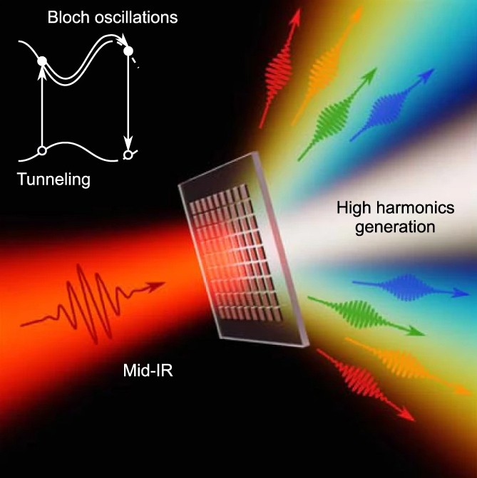
Cornell researchers have developed nanostructures that enable record-breaking conversion of laser pulses into high-harmonic generation, paving the way for new scientific tools for high-resolution imaging and studying physical processes that occur at the scale of an attosecond – one quintillionth of a second [emphasis mine].

High-harmonic generation has long been used to merge photons from a pulsing laser into one, ultrashort photon with much higher energy, producing extreme ultraviolet light and X-rays used for a variety of scientific purposes. Traditionally, gases have been used as sources of harmonics, but a research team led by Gennady Shvets, professor of applied and engineering physics in the College of Engineering, has shown that engineered nanostructures have a bright future for this application.

llustration of an infrared laser hitting a gallium-phosphide metsurface, which efficiently produces even and odd high-harmonic generation. Credit: Daniil Shilkin/Provided

A July 21, 2021 Cornell University news release by Syl Kacapyr (also on EurekAlert), which originated the news item, provides more detail about the nanostructures,

The nanostructures created by the team make up an ultrathin resonant gallium-phosphide metasurface that overcomes many of the usual problems associated with high-harmonic generation in gases and other solids. The gallium-phosphide material permits harmonics of all orders without reabsorbing them, and the specialized structure can interact with the laser pulse’s entire light spectrum.

“Achieving this required engineering of the metasurface’s structure using full-wave simulations,” Shcherbakov [Maxim Shcherbakov] said. “We carefully selected the parameters of the gallium-phosphide particles to fulfill this condition, and then it took a custom nanofabrication flow to bring it to light.”

The result is nanostructures capable of generating both even and odd harmonics – a limitation of most other harmonic materials – covering a wide range of photon energies between 1.3 and 3 electron volts. The record-breaking conversion efficiency enables scientists to observe molecular and electronic dynamics within a material with just one laser shot, helping to preserve samples that may otherwise be degraded by multiple high-powered shots.

The study is the first to observe high-harmonic generated radiation from a single laser pulse, which allowed the metasurface to withstand high powers – five to 10 times higher than previously shown in other metasurfaces.

“It opens up new opportunities to study matter at ultrahigh fields, a regime not readily accessible before,” Shcherbakov said. “With our method, we envision that people can study materials beyond metasurfaces, including but not limited to crystals, 2D materials, single atoms, artificial atomic lattices and other quantum systems.”

Now that the research team has demonstrated the advantages of using nanostructures for high-harmonic generation, it hopes to improve high-harmonic devices and facilities by stacking the nanostructures together to replace a solid-state source, such as crystals.

Here’s a link to and a citation for the paper,

Generation of even and odd high harmonics in resonant metasurfaces using single and multiple ultra-intense laser pulses by Maxim R. Shcherbakov, Haizhong Zhang, Michael Tripepi, Giovanni Sartorello, Noah Talisa, Abdallah AlShafey, Zhiyuan Fan, Justin Twardowski, Leonid A. Krivitsky, Arseniy I. Kuznetsov, Enam Chowdhury & Gennady Shvets. Nature Communications volume 12, Article number: 4185 DOI: https://doi.org/10.1038/s41467-021-24450-9 Published: 07 July 2021

This paper is open access.

Nano-photosynthesis in your brain as a stroke treatment?

A May 19, 2021 news item on phys.org sheds some light on a new approach to stroke treatments,

Blocked blood vessels in the brains of stroke patients prevent oxygen-rich blood from getting to cells, causing severe damage. Plants and some microbes produce oxygen through photosynthesis. What if there was a way to make photosynthesis happen in the brains of patients? Now, researchers reporting in ACS’ Nano Letters have done just that in cells and in mice, using blue-green algae and special nanoparticles, in a proof-of-concept demonstration.

A May 19, 2021 American Chemical Society (ACS) news release, which originated the news item, provides more information on strokes and how this new approach may prove useful,

Strokes result in the deaths of 5 million people worldwide every year, according to the World Health Organization. Millions more survive, but they often experience disabilities, such as difficulties with speech, swallowing or memory. The most common cause is a blood vessel blockage in the brain, and the best way to prevent permanent brain damage from this type of stroke is to dissolve or surgically remove the blockage as soon as possible. However, those options only work within a narrow time window after the stroke happens and can be risky. Blue-green algae, such as Synechococcus elongatus, have been studied previously to treat the lack of oxygen in heart tissue and tumors using photosynthesis. But the visible light needed to trigger the microbes can’t penetrate the skull, and although near-infrared light can pass through, it is insufficient to directly power photosynthesis. “Up-conversion” nanoparticles, often used for imaging, can absorb near-infrared photons and emit visible light. So, Lin Wang, Zheng Wang, Guobin Wang and colleagues at Huazhong University of Science and Technology wanted to see if they could develop a new approach that could someday be used for stroke patients by combining these parts — S. elongatus, nanoparticles and near-infrared light — in a new “nano-photosynthetic” system.

The researchers paired S. elongatus with neodymium up-conversion nanoparticles that transform tissue-penetrating near-infrared light to a visible wavelength that the microbes can use to photosynthesize. In a cell study, they found that the nano-photosynthesis approach reduced the number of neurons that died after oxygen and glucose deprivation. They then injected the microbes and nanoparticles into mice with blocked cerebral arteries and exposed the mice to near-infrared light. The therapy reduced the number of dying neurons, improved the animals’ motor function and even helped new blood vessels to start growing. Although this treatment is still in the animal testing stage, it has promise to advance someday toward human clinical trials, the researchers say.

The authors acknowledge funding from the National Key Basic Research Program of China, the National Natural Science Foundation of China, the Chinese Ministry of Education’s Science and Technology Program, the Major Scientific and Technological Innovation Projects in Hubei Province, and the Joint Fund of Ministry of Education for Equipment Pre-research.

Here’s a link to and a citation for the paper,

Oxygen-Generating Cyanobacteria Powered by Upconversion-Nanoparticles-Converted Near-Infrared Light for Ischemic Stroke Treatment by Jian Wang, Qiangfei Su, Qiying Lv, Bo Cai, Xiakeerzhati Xiaohalati, Guobin Wang, Zheng Wang, and Lin Wang. Nano Lett. 2021, 21, 11, 4654–4665 DOI: https://doi.org/10.1021/acs.nanolett.1c00719 Publication Date:May 19, 2021 © 2021 American Chemical Society

This paper is behind a paywall.

Memristors, it’s all about the oxides

I have one research announcement from China and another from the Netherlands, both of which concern memristors and oxides.

China

A May 17, 2021 news item on Nanowerk announces work, which suggests that memristors may not need to rely solely on oxides but could instead utilize light more gainfully,

Scientists are getting better at making neuron-like junctions for computers that mimic the human brain’s random information processing, storage and recall. Fei Zhuge of the Chinese Academy of Sciences and colleagues reviewed the latest developments in the design of these ‘memristors’ for the journal Science and Technology of Advanced Materials …

Computers apply artificial intelligence programs to recall previously learned information and make predictions. These programs are extremely energy- and time-intensive: typically, vast volumes of data must be transferred between separate memory and processing units. To solve this issue, researchers have been developing computer hardware that allows for more random and simultaneous information transfer and storage, much like the human brain.

Electronic circuits in these ‘neuromorphic’ computers include memristors that resemble the junctions between neurons called synapses. Energy flows through a material from one electrode to another, much like a neuron firing a signal across the synapse to the next neuron. Scientists are now finding ways to better tune this intermediate material so the information flow is more stable and reliable.

I had no success locating the original news release, which originated the news item, but have found this May 17, 2021 news item on eedesignit.com, which provides the remaining portion of the news release.

“Oxides are the most widely used materials in memristors,” said Zhuge. “But oxide memristors have unsatisfactory stability and reliability. Oxide-based hybrid structures can effectively improve this.”

Memristors are usually made of an oxide-based material sandwiched between two electrodes. Researchers are getting better results when they combine two or more layers of different oxide-based materials between the electrodes. When an electrical current flows through the network, it induces ions to drift within the layers. The ions’ movements ultimately change the memristor’s resistance, which is necessary to send or stop a signal through the junction.

Memristors can be tuned further by changing the compounds used for electrodes or by adjusting the intermediate oxide-based materials. Zhuge and his team are currently developing optoelectronic neuromorphic computers based on optically-controlled oxide memristors. Compared to electronic memristors, photonic ones are expected to have higher operation speeds and lower energy consumption. They could be used to construct next generation artificial visual systems with high computing efficiency.

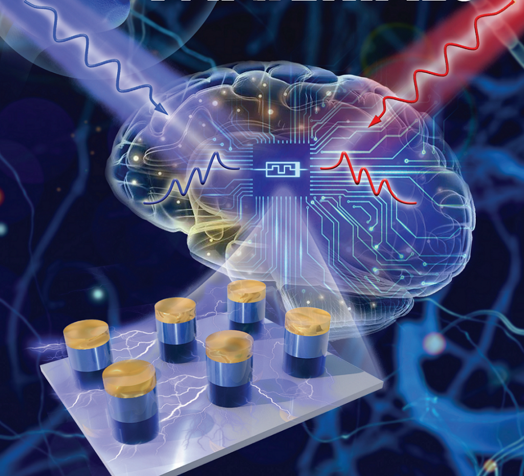
Now for a picture that accompanied the news release, which follows,

Fig. The all-optically controlled memristor developed for optoelectronic neuromorphic computing (Image by NIMTE)

Here’s the February 7, 2021 Ningbo Institute of Materials Technology and Engineering (NIMTE) press release featuring this work and a more technical description,

A research group led by Prof. ZHUGE Fei at the Ningbo Institute of Materials Technology and Engineering (NIMTE) of the Chinese Academy of Sciences (CAS) developed an all-optically controlled (AOC) analog memristor, whose memconductance can be reversibly tuned by varying only the wavelength of the controlling light.

As the next generation of artificial intelligence (AI), neuromorphic computing (NC) emulates the neural structure and operation of the human brain at the physical level, and thus can efficiently perform multiple advanced computing tasks such as learning, recognition and cognition.

Memristors are promising candidates for NC thanks to the feasibility of high-density 3D integration and low energy consumption. Among them, the emerging optoelectronic memristors are competitive by virtue of combining the advantages of both photonics and electronics. However, the reversible tuning of memconductance depends highly on the electric excitation, which have severely limited the development and application of optoelectronic NC.

To address this issue, researchers at NIMTE proposed a bilayered oxide AOC memristor, based on the relatively mature semiconductor material InGaZnO and a memconductance tuning mechanism of light-induced electron trapping and detrapping.

The traditional electrical memristors require strong electrical stimuli to tune their memconductance, leading to high power consumption, a large amount of Joule heat, microstructural change triggered by the Joule heat, and even high crosstalk in memristor crossbars.

On the contrary, the developed AOC memristor does not involve microstructure changes, and can operate upon weak light irradiation with light power density of only 20 μW cm-2, which has provided a new approach to overcome the instability of the memristor.

Specifically, the AOC memristor can serve as an excellent synaptic emulator and thus mimic spike-timing-dependent plasticity (STDP) which is an important learning rule in the brain, indicating its potential applications in AOC spiking neural networks for high-efficiency optoelectronic NC.

Moreover, compared to purely optical computing, the optoelectronic computing using our AOC memristor showed higher practical feasibility, on account of the simple structure and fabrication process of the device.

The study may shed light on the in-depth research and practical application of optoelectronic NC, and thus promote the development of the new generation of AI.

This work was supported by the National Natural Science Foundation of China (No. 61674156 and 61874125), the Strategic Priority Research Program of Chinese Academy of Sciences (No. XDB32050204), and the Zhejiang Provincial Natural Science Foundation of China (No. LD19E020001).

Here’s a link to and a citation for the paper,

Hybrid oxide brain-inspired neuromorphic devices for hardware implementation of artificial intelligence by Jingrui Wang, Xia Zhuge & Fei Zhuge. Science and Technology of Advanced Materials Volume 22, 2021 – Issue 1 Pages 326-344 DOI: https://doi.org/10.1080/14686996.2021.1911277 Published online:14 May 2021

This paper appears to be open access.

Netherlands

In this case, a May 18, 2021 news item on Nanowerk marries oxides to spintronics,

Classic computers use binary values (0/1) to perform. By contrast, our brain cells can use more values to operate, making them more energy-efficient than computers. This is why scientists are interested in neuromorphic (brain-like) computing.

Physicists from the University of Groningen (the Netherlands) have used a complex oxide to create elements comparable to the neurons and synapses in the brain using spins, a magnetic property of electrons.

The press release, which follows, was accompanied by this image illustrating the work,

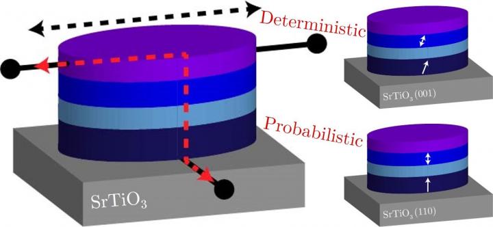
Caption: Schematic of the proposed device structure for neuromorphic spintronic memristors. The write path is between the terminals through the top layer (black dotted line), the read path goes through the device stack (red dotted line). The right side of the figure indicates how the choice of substrate dictates whether the device will show deterministic or probabilistic behaviour. Credit: Banerjee group, University of Groningen

A May 18, 2021 University of Groningen press release (also on EurekAlert), which originated the news item, adds more ‘spin’ to the story,

Although computers can do straightforward calculations much faster than humans, our brains outperform silicon machines in tasks like object recognition. Furthermore, our brain uses less energy than computers. Part of this can be explained by the way our brain operates: whereas a computer uses a binary system (with values 0 or 1), brain cells can provide more analogue signals with a range of values.

Thin films

The operation of our brains can be simulated in computers, but the basic architecture still relies on a binary system. That is why scientist look for ways to expand this, creating hardware that is more brain-like, but will also interface with normal computers. ‘One idea is to create magnetic bits that can have intermediate states’, says Tamalika Banerjee, Professor of Spintronics of Functional Materials at the Zernike Institute for Advanced Materials, University of Groningen. She works on spintronics, which uses a magnetic property of electrons called ‘spin’ to transport, manipulate and store information.

In this study, her PhD student Anouk Goossens, first author of the paper, created thin films of a ferromagnetic metal (strontium-ruthenate oxide, SRO) grown on a substrate of strontium titanate oxide. The resulting thin film contained magnetic domains that were perpendicular to the plane of the film. ‘These can be switched more efficiently than in-plane magnetic domains’, explains Goossens. By adapting the growth conditions, it is possible to control the crystal orientation in the SRO. Previously, out-of-plane magnetic domains have been made using other techniques, but these typically require complex layer structures.

Magnetic anisotropy

The magnetic domains can be switched using a current through a platinum electrode on top of the SRO. Goossens: ‘When the magnetic domains are oriented perfectly perpendicular to the film, this switching is deterministic: the entire domain will switch.’ However, when the magnetic domains are slightly tilted, the response is probabilistic: not all the domains are the same, and intermediate values occur when only part of the crystals in the domain have switched.

By choosing variants of the substrate on which the SRO is grown, the scientists can control its magnetic anisotropy. This allows them to produce two different spintronic devices. ‘This magnetic anisotropy is exactly what we wanted’, says Goossens. ‘Probabilistic switching compares to how neurons function, while the deterministic switching is more like a synapse.’

The scientists expect that in the future, brain-like computer hardware can be created by combining these different domains in a spintronic device that can be connected to standard silicon-based circuits. Furthermore, probabilistic switching would also allow for stochastic computing, a promising technology which represents continuous values by streams of random bits. Banerjee: ‘We have found a way to control intermediate states, not just for memory but also for computing.’

Here’s a link to and a citation for the paper,

Anisotropy and Current Control of Magnetization in SrRuO3/SrTiO3 Heterostructures for Spin-Memristors by A.S. Goossens, M.A.T. Leiviskä and T. Banerjee. Frontiers in Nanotechnology DOI: https://doi.org/10.3389/fnano.2021.680468 Published: 18 May 2021

This appears to be open access.

Will you be my friend? Yes, after we activate our ultraminiature, wireless, battery-free, fully implantable devices

Perhaps I’m the only one who’s disconcerted?

Here’s the research (in text form) as to why we’re watching these scampering, momentary mouse friends, from a May 10, 2021 Northwestern University news release (also on EurekAlert) by Amanda Morris,

Northwestern University researchers are building social bonds with beams of light.

For the first time ever, Northwestern engineers and neurobiologists have wirelessly programmed — and then deprogrammed — mice to socially interact with one another in real time. The advancement is thanks to a first-of-its-kind ultraminiature, wireless, battery-free and fully implantable device that uses light to activate neurons.

This study is the first optogenetics (a method for controlling neurons with light) paper exploring social interactions within groups of animals, which was previously impossible with current technologies.

The research was published May 10 [2021] in the journal Nature Neuroscience.

The thin, flexible, wireless nature of the implant allows the mice to look normal and behave normally in realistic environments, enabling researchers to observe them under natural conditions. Previous research using optogenetics required fiberoptic wires, which restrained mouse movements and caused them to become entangled during social interactions or in complex environments.

“With previous technologies, we were unable to observe multiple animals socially interacting in complex environments because they were tethered,” said Northwestern neurobiologist Yevgenia Kozorovitskiy, who designed the experiment. “The fibers would break or the animals would become entangled. In order to ask more complex questions about animal behavior in realistic environments, we needed this innovative wireless technology. It’s tremendous to get away from the tethers.”

“This paper represents the first time we’ve been able to achieve wireless, battery-free implants for optogenetics with full, independent digital control over multiple devices simultaneously in a given environment,” said Northwestern bioelectronics pioneer John A. Rogers, who led the technology development. “Brain activity in an isolated animal is interesting, but going beyond research on individuals to studies of complex, socially interacting groups is one of the most important and exciting frontiers in neuroscience. We now have the technology to investigate how bonds form and break between individuals in these groups and to examine how social hierarchies arise from these interactions.”

Kozorovitskiy is the Soretta and Henry Shapiro Research Professor of Molecular Biology and associate professor of neurobiology in Northwestern’s Weinberg College of Arts and Sciences. She also is a member of the Chemistry of Life Processes Institute. Rogers is the Louis Simpson and Kimberly Querrey Professor of Materials Science and Engineering, Biomedical Engineering and Neurological Surgery in the McCormick School of Engineering and Northwestern University Feinberg School of Medicine and the director of the Querrey Simpson Institute for Bioelectronics.

Kozorovitskiy and Rogers led the work with Yonggang Huang, the Jan and Marcia Achenbach Professor in Mechanical Engineering at McCormick, and Zhaoqian Xie, a professor of engineering mechanics at Dalian University of Technology in China. The paper’s co-first authors are Yiyuan Yang, Mingzheng Wu and Abraham Vázquez-Guardado — all at Northwestern.

Promise and problems of optogenetics

Because the human brain is a system of nearly 100 billion intertwined neurons, it’s extremely difficult to probe single — or even groups of — neurons. Introduced in animal models around 2005, optogenetics offers control of specific, genetically targeted neurons in order to probe them in unprecedented detail to study their connectivity or neurotransmitter release. Researchers first modify neurons in living mice to express a modified gene from light-sensitive algae. Then they can use external light to specifically control and monitor brain activity. Because of the genetic engineering involved, the method is not yet approved in humans.

“It sounds like sci-fi, but it’s an incredibly useful technique,” Kozorovitskiy said. “Optogenetics could someday soon be used to fix blindness or reverse paralysis.”

Previous optogenetics studies, however, were limited by the available technology to deliver light. Although researchers could easily probe one animal in isolation, it was challenging to simultaneously control neural activity in flexible patterns within groups of animals interacting socially. Fiberoptic wires typically emerged from an animal’s head, connecting to an external light source. Then a software program could be used to turn the light off and on, while monitoring the animal’s behavior.

“As they move around, the fibers tugged in different ways,” Rogers said. “As expected, these effects changed the animal’s patterns of motion. One, therefore, has to wonder: What behavior are you actually studying? Are you studying natural behaviors or behaviors associated with a physical constraint?”

Wireless control in real time

A world-renowned leader in wireless, wearable technology, Rogers and his team developed a tiny, wireless device that gently rests on the skull’s outer surface but beneath the skin and fur of a small animal. The half-millimeter-thick device connects to a fine, flexible filamentary probe with LEDs on the tip, which extend down into the brain through a tiny cranial defect.

The miniature device leverages near-field communication protocols, the same technology used in smartphones for electronic payments. Researchers wirelessly operate the light in real time with a user interface on a computer. An antenna surrounding the animals’ enclosure delivers power to the wireless device, thereby eliminating the need for a bulky, heavy battery.

Activating social connections

To establish proof of principle for Rogers’ technology, Kozorovitskiy and colleagues designed an experiment to explore an optogenetics approach to remote-control social interactions among pairs or groups of mice.

When mice were physically near one another in an enclosed environment, Kozorovitskiy’s team wirelessly synchronously activated a set of neurons in a brain region related to higher order executive function, causing them to increase the frequency and duration of social interactions. Desynchronizing the stimulation promptly decreased social interactions in the same pair of mice. In a group setting, researchers could bias an arbitrarily chosen pair to interact more than others.

“We didn’t actually think this would work,” Kozorovitskiy said. “To our knowledge, this is the first direct evaluation of a major long-standing hypothesis about neural synchrony in social behavior.”

Here’s a citation and a link to the paper,

Wireless multilateral devices for optogenetic studies of individual and social behaviors by Yiyuan Yang, Mingzheng Wu, Amy J. Wegener, Jose G. Grajales-Reyes, Yujun Deng, Taoyi Wang, Raudel Avila, Justin A. Moreno, Samuel Minkowicz, Vasin Dumrongprechachan, Jungyup Lee, Shuangyang Zhang, Alex A. Legaria, Yuhang Ma, Sunita Mehta, Daniel Franklin, Layne Hartman, Wubin Bai, Mengdi Han, Hangbo Zhao, Wei Lu, Yongjoon Yu, Xing Sheng, Anthony Banks, Xinge Yu, Zoe R. Donaldson, Robert W. Gereau IV, Cameron H. Good, Zhaoqian Xie, Yonggang Huang, Yevgenia Kozorovitskiy and John A. Rogers. Nature Neuroscience (2021)
DOI: https://doi.org/10.1038/s41593-021-00849-x Published 10 May 2021

This paper is behind a paywall.

This latest research seems to be the continuation of research featured here in a July 16, 2019 posting: “Controlling neurons with light: no batteries or wires needed.”

Nanosensors use AI to explore the biomolecular world

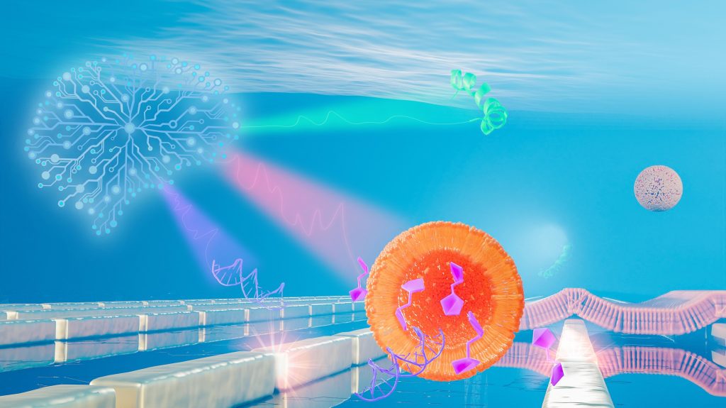
EPFL scientists have developed AI-powered nanosensors that let researchers track various kinds of biological molecules without disturbing them. Courtesy: École polytechnique fédérale de Lausanne (EPFL)

If you look at the big orange dot (representing the nanosensors?), you’ll see those purplish/fuschia objects resemble musical notes (biological molecules?). I think that brainlike object to the left and in light blue is the artificial intelligence (AI) component. (If anyone wants to correct my guesses or identify the bits I can’t, please feel free to add to the Comments for this blog.)

Getting back to my topic, keep the ‘musical notes’ in mind as you read about some of the latest research from l’École polytechnique fédérale de Lausanne (EPFL) in an April 7, 2021 news item on Nanowerk,

The tiny world of biomolecules is rich in fascinating interactions between a plethora of different agents such as intricate nanomachines (proteins), shape-shifting vessels (lipid complexes), chains of vital information (DNA) and energy fuel (carbohydrates). Yet the ways in which biomolecules meet and interact to define the symphony of life is exceedingly complex.

Scientists at the Bionanophotonic Systems Laboratory in EPFL’s School of Engineering have now developed a new biosensor that can be used to observe all major biomolecule classes of the nanoworld without disturbing them. Their innovative technique uses nanotechnology, metasurfaces, infrared light and artificial intelligence.

To each molecule its own melody

In this nano-sized symphony, perfect orchestration makes physiological wonders such as vision and taste possible, while slight dissonances can amplify into horrendous cacophonies leading to pathologies such as cancer and neurodegeneration.

An April 7, 2021 EPFL press release, which originated the news item, provides more detail,

“Tuning into this tiny world and being able to differentiate between proteins, lipids, nucleic acids and carbohydrates without disturbing their interactions is of fundamental importance for understanding life processes and disease mechanisms,” says Hatice Altug, the head of the Bionanophotonic Systems Laboratory. 

Light, and more specifically infrared light, is at the core of the biosensor developed by Altug’s team. Humans cannot see infrared light, which is beyond the visible light spectrum that ranges from blue to red. However, we can feel it in the form of heat in our bodies, as our molecules vibrate under the infrared light excitation.

Molecules consist of atoms bonded to each other and – depending on the mass of the atoms and the arrangement and stiffness of their bonds – vibrate at specific frequencies. This is similar to the strings on a musical instrument that vibrate at specific frequencies depending on their length. These resonant frequencies are molecule-specific, and they mostly occur in the infrared frequency range of the electromagnetic spectrum. 

“If you imagine audio frequencies instead of infrared frequencies, it’s as if each molecule has its own characteristic melody,” says Aurélian John-Herpin, a doctoral assistant at Altug’s lab and the first author of the publication. “However, tuning into these melodies is very challenging because without amplification, they are mere whispers in a sea of sounds. To make matters worse, their melodies can present very similar motifs making it hard to tell them apart.” 

Metasurfaces and artificial intelligence

The scientists solved these two issues using metasurfaces and AI. Metasurfaces are man-made materials with outstanding light manipulation capabilities at the nano scale, thereby enabling functions beyond what is otherwise seen in nature. Here, their precisely engineered meta-atoms made out of gold nanorods act like amplifiers of light-matter interactions by tapping into the plasmonic excitations resulting from the collective oscillations of free electrons in metals. “In our analogy, these enhanced interactions make the whispered molecule melodies more audible,” says John-Herpin.

AI is a powerful tool that can be fed with more data than humans can handle in the same amount of time and that can quickly develop the ability to recognize complex patterns from the data. John-Herpin explains, “AI can be imagined as a complete beginner musician who listens to the different amplified melodies and develops a perfect ear after just a few minutes and can tell the melodies apart, even when they are played together – like in an orchestra featuring many instruments simultaneously.” 

The first biosensor of its kind

When the scientists’ infrared metasurfaces are augmented with AI, the new sensor can be used to analyze biological assays featuring multiple analytes simultaneously from the major biomolecule classes and resolving their dynamic interactions. 

“We looked in particular at lipid vesicle-based nanoparticles and monitored their breakage through the insertion of a toxin peptide and the subsequent release of vesicle cargos of nucleotides and carbohydrates, as well as the formation of supported lipid bilayer patches on the metasurface,” says Altug.

This pioneering AI-powered, metasurface-based biosensor will open up exciting perspectives for studying and unraveling inherently complex biological processes, such as intercellular communication via exosomesand the interaction of nucleic acids and carbohydrates with proteins in gene regulation and neurodegeneration. 

“We imagine that our technology will have applications in the fields of biology, bioanalytics and pharmacology – from fundamental research and disease diagnostics to drug development,” says Altug. 

Here’s a link to and a citation for the paper,

Infrared Metasurface Augmented by Deep Learning for Monitoring Dynamics between All Major Classes of Biomolecules by Aurelian John‐Herpin, Deepthy Kavungal. Lea von Mücke, Hatice Altug. Advanced Materials Volume 33, Issue 14 April 8, 2021 2006054 DOI: https://doi.org/10.1002/adma.202006054 First published: 22 February 2021

This paper is open access.