Monthly Archives: June 2015

Call for AAAS Kavli science journalism award submission goes international, for the first time

From a June 22, 2015 American Association for the Advancement of Science (AAAS) news release in my mailbox,

The contest year for the 2015 AAAS Kavli Science Journalism Awards will close on 15 July. Be sure to enter your best work that appeared in print, online or on air between 1 July 2014 and 15 July 2015. The entry deadline is August 1, 2015. [emphasis mine]

Thanks to an expanded endowment from The Kavli Foundation, the competition is open for the first time to professional journalists from around the world in each of the eight reporting categories. There is no entry fee. Please read the Contest Rules and Frequently Asked Questions before submitting.

Note: If the submitted work was published or broadcast in a language other than English, you must provide an English translation.

The awards recognize outstanding reporting for a general audience and honor individuals for coverage of the sciences, engineering, and mathematics. Stories on the environment, energy, science policy, and health qualify if they deal in a substantive way with underlying science. Independent committees of journalists select the winning entries.

The categories:
·  Large Newspaper (circulation of 150,000 or more, daily or weekly)
·  Small Newspaper (circulation of less than 150,000, daily or weekly)
·  Magazine
·  TV – Spot News/Feature Reporting (20 minutes or less)
·  TV – In-Depth Reporting (more than 20 minutes)
·  Radio
·  Online
·  Children’s Science News (reporting on science for children, including young teens up to age 14)

You can find Contest Rules here and you can find Frequently Asked Questions (FAQs) here,

Q: I work for a state-funded news organization. Am I eligible?

A. The news outlet must be editorially independent. Questions about eligibility are decided by the awards administrator in consultation with the Managing Committee (an advisory panel of science journalists.)

Q. Are commentaries or articles in advocacy publications eligible for the award?

A. No.

Q. Are books eligible?

No, books, book chapters and e-books are not eligible.

Q. Are stories written by public information officers or freelancers for university-funded research magazines or Web sites eligible for the awards?

A. No. The Managing Committee has determined that such publications are not eligible for the awards.

Q. Are podcasts eligible for the award?

A. Some podcasts are eligible for consideration within the Online category. They must be science-news-only podcasts aimed at a general audience and prepared by reporters. Institutional podcasts from university news or research offices, or podcasts featuring news as well as other types of segments are not eligible.

Q. Are blogs eligible?

A. Yes, in the “Online” category. The judges will determine whether a blog entry meets the standards of professional journalism and is accessible to a general audience.

Finally, you can make your submission by clicking the link on this page which includes a summary of the rules and FAQs.

Good luck!

Customizing bacteria (E. coli) into squares, circles, triangles, etc.

The academic paper for this latest research from Delft University of Technology (TU Delft, Netherlands), uses the term ‘bacterial sculptures,’ an intriguing idea that seems to have influenced the artistic illustration accompanying the research announcement.

Artistic rendering live E.coli bacteria that have been shaped into a rectangle, triangle, circle, and square (from front to back). Colors indicate the density of the Min proteins that represent a snapshot in time (based on actual data), as these proteins oscillate back and forth within the bacterium, to determine the mid plane of the cell for cellular division. Image credit:  ‘Image Cees Dekker lab TU Delft / Tremani’

Artistic rendering live E.coli bacteria that have been shaped into a rectangle, triangle, circle, and square (from front to back). Colors indicate the density of the Min proteins that represent a snapshot in time (based on actual data), as these proteins oscillate back and forth within the bacterium, to determine the mid plane of the cell for cellular division.
Image credit: ‘Image Cees Dekker lab TU Delft / Tremani’

A June 22, 2015 news item on Nanowerk provides more insight into the research (Note: A link has been removed),

The E.coli bacterium, a very common resident of people’s intestines, is shaped as a tiny rod about 3 micrometers long. For the first time, scientists from the Kavli Institute of Nanoscience at Delft University have found a way to use nanotechnology to grow living E.coli bacteria into very different shapes: squares, triangles, circles, and even as letters spelling out ‘TU Delft’. They also managed to grow supersized E.coli with a volume thirty times larger than normal. These living oddly-shaped bacteria allow studies of the internal distribution of proteins and DNA in entirely new ways.

In this week’s Nature Nanotechnology (“Symmetry and scale orient Min protein patterns in shaped bacterial sculptures”), the scientists describe how these custom-designed bacteria still manage to perfectly locate ‘the middle of themselves’ for their cell division. They are found to do so using proteins that sense the cell shape, based on a mathematical principle proposed by computer pioneer Alan Turing in 1953.

A June 22, 2015 TU Delft press release, which originated the news item, expands on the theme,

Cell division

“If cells can’t divide properly, biological life wouldn’t be possible. Cells need to distribute their cell volume and genetic materials equally into their daughter cells to proliferate.”, says prof. Cees Dekker, “It is fascinating that even a unicellular organism knows how to divide very precisely. The distribution of certain proteins in the cell is key to regulating this, but how exactly do those proteins get that done?”

Turing

As the work of the Delft scientist exemplifies, the key here is a process discovered by the famous Alan Turing in 1953. Although Turing is mostly known for his role in deciphering the Enigma coding machine and the Turing Test, the impact of his ‘reaction-diffusion theory’ on biology might be even more spectacular. He predicted how patterns in space and time emerge as the result of only two molecular interactions – explaining for instance how a zebra gets its stripes, or how an embryo hand develops five fingers.

MinD and MinE

Such a Turing process also acts with proteins within a single cell, to regulate cell division. An E.coli cell uses two types of proteins, known as MinD and MinE, that bind and unbind again and again at the inner surface of the bacterium, thus oscillating back and forth from pole to pole within the bacterium every minute. “This results in a low average concentration of the protein in the middle and high concentrations at the ends, which drives the division machinery to the cell center”, says PhD-student Fabai Wu, who ran the experiments. “As our experiments show, the Turing patterns allow the bacterium to determine its symmetry axes and its center. This applies to many bacterial cell shapes that we custom-designed, such as squares, triangles and rectangles of many sizes. For fun, we even made ‘TUDelft’ and ‘TURING’ letters. Using computer simulations, we uncovered that the shape-sensing abilities are caused by simple Turing-type interactions between the proteins.”

Actual data for live E.coli bacteria that have been shaped into the letters TUDELFT.
The red color shows the cytosol contents of the cell, while the green color shows the density of the Min proteins, representing a snapshot in time, as these proteins oscillate back and forth within the bacterium to determine the mid plane of the cell for cellular division. The letters are about 5 micron high.
Image credit:  ‘Fabai Wu, Cees Dekker lab at TU Delft’

Spatial control for building synthetic cells

“Discovering this process is not only vital for our understanding of bacterial cell division – which is important in developing new strategies for antibiotics. But the approach will likely also be fruitful to figuring out how cells distribute other vital systems within a cell, such as chromosomes”, says Cees Dekker. “The ultimate goal in our research is to be able to completely build a living cell from artificial components, as that is the only way to really understand how life works. Understanding cell division – both the process that actually pinches off the cell into two daughters and the part that spatially regulates that machinery – is a major part of that.”

Here’s a link to and a citation for the paper,

Symmetry and scale orient Min protein patterns in shaped bacterial sculptures by Fabai Wu, Bas G. C. van Schie, Juan E. Keymer, & Cees Dekker. Nature Nanotechnology (2015) doi:10.1038/nnano.2015.126 Published online 22 June 2015

This paper is behind a paywall but there does seem to be another link (in the excerpt below) which gives you a free preview via ReadCube Access (according to the TU Delft press release),

The DOI for this paper will be 10.1038/nnano.2015.126. Once the paper is published electronically, the DOI can be used to retrieve the abstract and full text by adding it to the following url: http://dx.doi.org/

Enjoy!

New US government nano commercialization effort: nanosensors

The latest announcement (this one about nanosensors) from the US National Nanotechnology Coordination Office (NNCO) on behalf of the US National Nanotechnology (NNI) gets a little confusing but hopefully I’ve managed to clarify things.

It starts off simply enough, from a June 22, 2015 news item on Azonano,

The National Nanotechnology Coordination Office (NNCO) is pleased to announce the launch of a workshop report and a web portal, efforts coordinated through and in support of the Nanotechnology Signature Initiative ‘Nanotechnology for Sensors and Sensors for Nanotechnology: Improving and Protecting Health, Safety, and the Environment’ (Sensors NSI). Together, these resources help pave the path forward for the development and commercialization of nanotechnology-enabled sensors and sensors for nanotechnology.

A June 19, 2015 NNCO news release on EurekAlert, which originated the news item, provides details about the report, the new portal, and the new series of webinars,

The workshop report is a summary of the National Nanotechnology Initiative (NNI)-sponsored event held September 11-12, 2014, entitled ‘Sensor Fabrication, Integration, and Commercialization Workshop.’ The goal of the workshop was to identify and discuss challenges that are faced by the sensor development community during the fabrication, integration, and commercialization of sensors, particularly those employing or addressing issues of nanoscale materials and technologies.

Workshop attendees, including sensor developers and representative from Federal agencies, identified ways to help facilitate the commercialization of nanosensors, which include:

  • Enhancing communication among researchers, developers, manufacturers, customers, and the Federal Government agencies that support and regulate sensor development.
  • Leveraging resources by building testbeds for sensor developers.
  • Improving access of university and private researchers to federally supported facilities.
  • Encouraging sensor developers to consider and prepare for market and regulatory requirements early in the development process.

In response to discussions at the workshop, the NNI has also launched an NSI Sensors web portal to share information on the sensors development landscape, including funding agencies and opportunities, federally supported facilities, regulatory guidance, and published standards. Ongoing dialogue and collaboration among various stakeholder groups will be critical to effectively transitioning nanosensors to market and to meeting the U.S. need for a reliable and robust sensor infrastructure.

On Thursday June 25, 2015, from noon to 1 pm EDT, NNCO will host a webinar to summarize the highlights from the 2014 ‘Sensor Fabrication, Integration, and Commercialization Workshop’ and to introduce the newly developed Sensors NSI Web Portal. The webinar will also feature a Q&A segment with members of the public. Questions for the panel can be submitted to webinar@nnco.nano.gov from June 18 through the end of the webinar at 1 pm EDT on June 25, 2015.

Here’s the portal for what they’ve called the NSI [Nanotechnology Signature Initiative]: Nanotechnology for Sensors and Sensors for Nanotechnology — Improving and Protecting, Health Safety, and the Environment, also known as, Sensors NSI Web Portal.

Here’s the report titled, “Sensor Fabrication, Integration, and Commercialization Workshop [2014].”

As for the first webinar in this new series, from the National Signature Webinar Series: Resources for the Development of Nanosensors webpage,

The National Nanotechnology Coordination Office (NNCO) will host a webinar to summarize the highlights from the September 2014 Sensor Fabrication, Integration, and Commercialization Workshop and to introduce the newly developed Sensors NSI Web Portal, which was created to share information on the sensors development landscape, including Federal program and funding opportunities, federally supported facilities, regulatory guidance, and published standards.

On Thursday, June 25, 2015, from 12 noon to 1 pm EDT, Federal panelists will begin the event with a discussion of the findings from the Sensor Fabrication, Integration, and Commercialization Workshop, as well as a demonstration of the resources available on the Sensors NSI Portal.  [emphasis mine]

Federal panelists at the event will include:

This event will feature a Q&A segment with members of the public. Questions for the panel can be submitted to webinar@nnco.nano.gov from June 18 through the end of the webinar at 1 pm on June 25, 2015. The moderator reserves the right to group similar questions and to omit questions that are either repetitive or not directly related to the topic. Due to time constraints, it may not be possible to answer all questions.

You can find the link to register at the end/bottom of the event page.

The NNCO does have one other Public Webinar series, ‘NNCO Small- and Medium-sized Business Enterprise (SME) Webinar Series’. They have archived previously held webinars in this series. There are no upcoming webinars in this series currently scheduled.

Making carbon nanoparticles at home with honey or molasses

No need to rush and buy any ingredients as the University of Illinois at Urbana-Champaign researchers do not provide a recipe for cooking up carbon nanoparticles. However, it is diverting to think that one day we might be able to make these items at home. From a June 19, 2015 news item by Stuart Milne on the Azonano website,

Researchers at the University of Illinois have discovered an easy method to produce carbon nanoparticles for biomedical applications. These carbon nanoparticles can be made at home within a couple of hours using easily available ingredients and molasses.

A June 19 (?), 2015 University of Illinois at Urbana-Champaign news release (also on EurekAlert) provides more detail about the research,

“If you have a microwave and honey or molasses, you can pretty much make these particles at home,” Pan [professor Dipanjan Pan] said. “You just mix them together and cook it for a few minutes, and you get something that looks like char, but that is nanoparticles with high luminescence. This is one of the simplest systems that we can think of. It is safe and highly scalable for eventual clinical use.”

These “next-generation” carbon spheres have several attractive properties, the researchers found. They naturally scatter light in a manner that makes them easy to differentiate from human tissues, eliminating the need for added dyes or fluorescing molecules to help detect them in the body.

The nanoparticles are coated with polymers that fine-tune their optical properties and their rate of degradation in the body. The polymers can be loaded with drugs that are gradually released.

The nanoparticles also can be made quite small, less than eight nanometers in diameter (a human hair is 80,000 to 100,000 nanometers thick).

“Our immune system fails to recognize anything under 10 nanometers,” Pan said. “So, these tiny particles are kind of camouflaged, I would say; they are hiding from the human immune system.”

The team tested the therapeutic potential of the nanoparticles by loading them with an anti-melanoma drug and mixing them in a topical solution that was applied to pig skin.

Bhargava’s [professor Rohit Bhargava] laboratory used vibrational spectroscopic techniques to identify the molecular structure of the nanoparticles and their cargo.

“Raman and infrared spectroscopy are the two tools that one uses to see molecular structure,” Bhargava said. “We think we coated this particle with a specific polymer and with specific drug-loading – but did we really? We use spectroscopy to confirm the formulation as well as visualize the delivery of the particles and drug molecules.”

The team found that the nanoparticles did not release the drug payload at room temperature, but at body temperature began to release the anti-cancer drug. The researchers also determined which topical applications penetrated the skin to a desired depth.

In further experiments, the researchers found they could alter the infusion of the particles into melanoma cells by adjusting the polymer coatings. Imaging confirmed that the infused cells began to swell, a sign of impending cell death.

“This is a versatile platform to carry a multitude of drugs – for melanoma, for other kinds of cancers and for other diseases,” Bhargava said. “You can coat it with different polymers to give it a different optical response. You can load it with two drugs, or three, or four, so you can do multidrug therapy with the same particles.”

“By using defined surface chemistry, we can change the properties of these particles,” Pan said. “We can make them glow at a certain wavelength and also we can tune them to release the drugs in the presence of the cellular environment. That is, I think, the beauty of the work.”

Here’s a link to and a citation for the paper,

Tunable Luminescent Carbon Nanospheres with Well-Defined Nanoscale Chemistry for Synchronized Imaging and Therapy by Prabuddha Mukherjee, Santosh K. Misra, Mark C. Gryka, Huei-Huei Chang, Saumya Tiwari, William L. Wilson, John W. Scott, Rohit Bhargava, and Dipanjan Pan. Small
DOI: 10.1002/smll.201500728 Article first published online: 20 MAY 2015

© 2015 WILEY-VCH Verlag GmbH & Co. KGaA, Weinheim

This paper is behind a paywall.

Saharan silver ants: the nano of it all (science and technology)

Researchers at Columbia University (US) are on quite a publishing binge lately. The latest is a biomimicry story where researchers (from Columbia amongst other universities and including Brookhaven National Laboratory, which has issued its own news release) have taken a very close look at Saharan silver ants to determine how they stay cool in one of the hottest climates in the world. From a June 18, 2015 Columbia University news release (also on EurekAlert), Note: Links have been removed,

Nanfang Yu, assistant professor of applied physics at Columbia Engineering, and colleagues from the University of Zürich and the University of Washington, have discovered two key strategies that enable Saharan silver ants to stay cool in one of the hottest terrestrial environments on Earth. Yu’s team is the first to demonstrate that the ants use a coat of uniquely shaped hairs to control electromagnetic waves over an extremely broad range from the solar spectrum (visible and near-infrared) to the thermal radiation spectrum (mid-infrared), and that different physical mechanisms are used in different spectral bands to realize the same biological function of reducing body temperature. Their research, “Saharan silver ants keep cool by combining enhanced optical reflection and radiative heat dissipation,” is published June 18 [2015] in Science magazine.

The Columbia University news release expands on the theme,

“This is a telling example of how evolution has triggered the adaptation of physical attributes to accomplish a physiological task and ensure survival, in this case to prevent Saharan silver ants from getting overheated,” Yu says. “While there have been many studies of the physical optics of living systems in the ultraviolet and visible range of the spectrum, our understanding of the role of infrared light in their lives is much less advanced. Our study shows that light invisible to the human eye does not necessarily mean that it does not play a crucial role for living organisms.”

The project was initially triggered by wondering whether the ants’ conspicuous silvery coats were important in keeping them cool in blistering heat. Yu’s team found that the answer to this question was much broader once they realized the important role of infrared light. Their discovery that there is a biological solution to a thermoregulatory problem could lead to the development of novel flat optical components that exhibit optimal cooling properties.

“Such biologically inspired cooling surfaces will have high reflectivity in the solar spectrum and high radiative efficiency in the thermal radiation spectrum,” Yu explains. “So this may generate useful applications such as a cooling surface for vehicles, buildings, instruments, and even clothing.”

Saharan silver ants (Cataglyphis bombycina) forage in the Saharan Desert in the full midday sun when surface temperatures reach up to 70°C (158°F), and they must keep their body temperature below their critical thermal maximum of 53.6°C (128.48°F) most of the time. In their wide-ranging foraging journeys, the ants search for corpses of insects and other arthropods that have succumbed to the thermally harsh desert conditions, which they are able to endure more successfully. Being most active during the hottest moment of the day also allows these ants to avoid predatory desert lizards. Researchers have long wondered how these tiny insects (about 10 mm, or 3/8” long) can survive under such thermally extreme and stressful conditions.

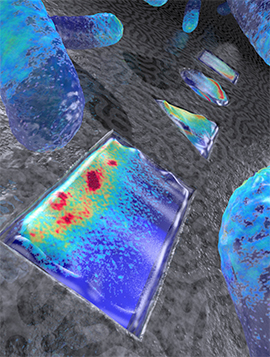
Using electron microscopy and ion beam milling, Yu’s group discovered that the ants are covered on the top and sides of their bodies with a coating of uniquely shaped hairs with triangular cross-sections that keep them cool in two ways. These hairs are highly reflective under the visible and near-infrared light, i.e., in the region of maximal solar radiation (the ants run at a speed of up to 0.7 meters per second and look like droplets of mercury on the desert surface). The hairs are also highly emissive in the mid-infrared portion of the electromagnetic spectrum, where they serve as an antireflection layer that enhances the ants’ ability to offload excess heat via thermal radiation, which is emitted from the hot body of the ants to the cold sky. This passive cooling effect works under the full sun whenever the insects are exposed to the clear sky.

“To appreciate the effect of thermal radiation, think of the chilly feeling when you get out of bed in the morning,” says Yu. “Half of the energy loss at that moment is due to thermal radiation since your skin temperature is temporarily much higher than that of the surrounding environment.”

The researchers found that the enhanced reflectivity in the solar spectrum and enhanced thermal radiative efficiency have comparable contributions to reducing the body temperature of silver ants by 5 to 10 degrees compared to if the ants were without the hair cover. “The fact that these silver ants can manipulate electromagnetic waves over such a broad range of spectrum shows us just how complex the function of these seemingly simple biological organs of an insect can be,” observes Norman Nan Shi, lead author of the study and PhD student who works with Yu at Columbia Engineering.

Yu and Shi collaborated on the project with Rüdiger Wehner, professor at the Brain Research Institute, University of Zürich, Switzerland, and Gary Bernard, electrical engineering professor at the University of Washington, Seattle, who are renowned experts in the study of insect physiology and ecology. The Columbia Engineering team designed and conducted all experimental work, including optical and infrared microscopy and spectroscopy experiments, thermodynamic experiments, and computer simulation and modeling. They are currently working on adapting the engineering lessons learned from the study of Saharan silver ants to create flat optical components, or “metasurfaces,” that consist of a planar array of nanophotonic elements and provide designer optical and thermal radiative properties.

Yu and his team plan next to extend their research to other animals and organisms living in extreme environments, trying to learn the strategies these creatures have developed to cope with harsh environmental conditions.

“Animals have evolved diverse strategies to perceive and utilize electromagnetic waves: deep sea fish have eyes that enable them to maneuver and prey in dark waters, butterflies create colors from nanostructures in their wings, honey bees can see and respond to ultraviolet signals, and fireflies use flash communication systems,” Yu adds. “Organs evolved for perceiving or controlling electromagnetic waves often surpass analogous man-made devices in both sophistication and efficiency. Understanding and harnessing natural design concepts deepens our knowledge of complex biological systems and inspires ideas for creating novel technologies.”

Next, there’s the perspective provided by Brookhaven National Laboratory in a June 18, 2015 news item on Nanowerk (Note: It is very similar to the Columbia University news release but it takes a turn towards the technical challenges as you’ll see if you keep reading),

The paper, published by Columbia Engineering researchers and collaborators—including researchers from the U.S. Department of Energy’s (DOE) Brookhaven National Laboratory—describes how the nanoscale structure of the hairs helps increase the reflectivity of the ant’s body in both visible and near-infrared wavelengths, allowing the insects to deflect solar radiation their bodies would otherwise absorb. The hairs also enhance emissivity in the mid-infrared spectrum, allowing heat to dissipate efficiently from the hot body of the ants to the cool, clear sky.

A June 18, 2015 BNL news release by Alasdair Wilkins, which originated the Nanowerk news item, describes the collaboration between the researchers and the special adjustments made to the equipment in service of this project (Note: A link has been removed),

In a typical experiment involving biological material such as nanoscale hairs, it would usually be sufficient to use an electron microscope to create an image of the surface of the specimen. This research, however, required Yu’s group to look inside the ant hairs and produce a cross-section of the structure’s interior. The relatively weak beam of electrons from a standard electron microscope would not be able to penetrate the surface of the sample.

The CFN’s dual beam system solves the problem by combining the imaging of an electron microscope with a much more powerful beam of gallium ions.  With 31 protons and 38 neutrons, each gallium ion is about 125,000 times more massive than an electron, and massive enough to create dents in the nanoscale structure – like throwing a stone against a wall. The researchers used these powerful beams to drill precise cuts into the hairs, revealing the crucial information hidden beneath the surface. Indeed, this particular application, in which the system was used to investigate a biological problem, was new for the team at CFN.

“Conventionally, this tool is used to produce cross-sections of microelectronic circuits,” said Camino. “The focused ion beam is like an etching tool. You can think of it like a milling tool in a machine shop, but at the nanoscale. It can remove material at specific places because you can see these locations with the SEM. So locally you remove material and you look at the under layers, because the cuts give you access to the cross section of whatever you want to look at.”

The ant hair research challenged the CFN team to come up with novel solutions to investigate the internal structures without damaging the more delicate biological samples.

“These hairs are very soft compared to, say, semiconductors or crystalline materials. And there’s a lot of local heat that can damage biological samples. So the parameters have to be carefully tuned not to do much damage to it,” he said. “We had to adapt our technique to find the right conditions.”

Another challenge lay in dealing with the so-called charging effect. When the dual beam system is trained on a non-conducting material, electrons can build up at the point where the beams hit the specimen, distorting the resulting image. The team at CFN was able to solve this problem by placing thin layers of gold over the biological material, making the sample just conductive enough to avoid the charging effect.

Revealing Reflectivity

While Camino’s team focused on helping Yu’s group investigate the structure of the ant hairs, Matthew Sfeir’s work with high-brightness Fourier transform optical spectroscopy helped to reveal how the reflectivity of the hairs helped Saharan silver ants regulate temperature. Sfeir’s spectrometer revealed precisely how much those biological structures reflect light across multiple wavelengths, including both visible and near-infrared light.

“It’s a multiplexed measurement,” Sfeir said, explaining his team’s spectrometer. “Instead of tuning through this wavelength and this wavelength, that wavelength, you do them all in one swoop to get all the spectral information in one shot. It gives you very fast measurements and very good resolution spectrally. Then we optimize it for very small samples. It’s a rather unique capability of CFN.”

Sfeir’s spectroscopy work draws on knowledge gained from his work at another key Brookhaven facility: the original National Synchrotron Light Source, where he did much of his postdoc work. His experience was particularly useful in analyzing the reflectivity of the biological structures across many different wavelengths of the electromagnetic spectrum.

“This technique was developed from my experience working with the infrared synchrotron beamlines,” said Sfeir. “Synchrotron beamlines are optimized for exactly this kind of thing. I thought, ‘Hey, wouldn’t it be great if we could develop a similar measurement for the type of solar devices we make at CFN?’ So we built a bench-top version to use here.”

Fascinating, non? At last, here’s a link to and a citation for the paper,

Keeping cool: Enhanced optical reflection and heat dissipation in silver ants by Norman Nan Shi, Cheng-Chia Tsai, Fernando Camino, Gary D. Bernard, Nanfang Yu, and Rüdiger Wehner. Science DOI: 10.1126/science.aab3564 Published online June 18, 2015

This paper is behind a paywall.

Nanoscale imaging gets rough

Smooth is easier than rough when imaging at the nanoscale according to a June 17, 2015 Northwestern University news release by Megan Fellman (also on EurekAlert),

A multi-institutional team of scientists has taken an important step in understanding where atoms are located on the surfaces of rough materials, information that could be very useful in diverse commercial applications, such as developing green energy and understanding how materials rust.

Researchers from Northwestern University, Brookhaven National Laboratory, Lawrence Berkeley National Laboratory and the University of Melbourne, Australia, have developed a new imaging technique that uses atomic resolution secondary electron images in a quantitative way to determine the arrangement of atoms on the surface.

Many important processes take place at surfaces, ranging from the catalysis used to generate energy-dense fuels from sunlight and carbon dioxide to how bridges and airplanes corrode, or rust. Every material interacts with the world through its surface, which is often different in both structure and chemistry from the bulk of the material.

The real focus of the work is on corrosion, according to the news release,

“We are excited by the possibilities of applying our imaging technique to corrosion and catalysis problems,” said Laurence Marks, a co-author of the paper and a professor of materials science and engineering at Northwestern’s McCormick School of Engineering and Applied Science. “The cost of corrosion to industry and the military is enormous, and we do not understand everything that is taking place. We must learn more, so we can produce materials that will last longer.”

To understand these processes and improve material performance, it is vital to know how the atoms are arranged on surfaces. While there are many good methods for obtaining this information for rather flat surfaces, most currently available tools are limited in what they can reveal when the surfaces are rough.

Scanning electron microscopes are widely used to produce images of many different materials, and roughness of the surface is not that important. Until very recently, instruments could not obtain clear atomic images of surfaces until a group at Brookhaven managed in 2011 to get the first images that seemed to show the surfaces very clearly. However, it was not clear to what extent they really were able to image the surface, as there was no theory for the imaging and many uncertainties.

The new work has answered all these questions, Marks said, providing a definitive way of understanding the surfaces in detail. What was needed was to use a carefully controlled sample of strontium titanate and perform a large range of different types of imaging to unravel the precise details of how secondary electron images are produced.

“We started this work by investigating a well-studied material,” said Jim Ciston, a staff scientist at Lawrence Berkeley National Laboratory and the lead author of the paper, who obtained the experimental images. “This new technique is so powerful that we had to revise much of what was already thought to be well-known. This is an exciting prospect because the surface of every material can act as its own nanomaterial coating, which can greatly change the chemistry and behavior.”

“The beauty of the technique is that we can image surface atoms and bulk atoms simultaneously,” said Yimei Zhu, a scientist at Brookhaven National Laboratory. “Currently, no existing methods can achieve that.”

Les Allen, who led the theoretical and modeling aspects of the new imaging technique in Melbourne, said, “We now have a sophisticated understanding of what the images mean. It now will be full steam ahead to apply them to many different types of problems.”

Here’s a link to and citation for the paper,

Surface determination through atomically resolved secondary-electron imaging by J. Ciston, H. G. Brown, A. J. D’Alfonso, P. Koirala, C. Ophus, Y. Lin, Y. Suzuki, H. Inada, Y. Zhu, L. J. Allen, & L. D. Marks. Nature Communications 6, Article number: 7358 doi:10.1038/ncomms8358 Published 17 June 2015

This paper is open access.

US White House Office of Science and Technology Policy issues a Nanotechnology Grand Challenges request for information

First, there was the Bill and Melinda Gates Foundation Grand Challenges, then there was some sort of Canadian government Grand Challenges, and now there’s the US government Nanotechnology-Inspired Grand Challenges for the Next Decade.

I find it fascinating that ‘Grand Challenges’ have become so popular given the near certainty of at least one defeat and the possibility the entire project will fail. By definition, it’s not a challenge if it’s an easy accomplishment.

Enough musing, a June 18, 2015 news item on Azonano announces the US government (White House Office of Science and Technology Policy [OSTP]) request for information (RFI), which has a deadline of July 16, 2015,

The National Nanotechnology Coordination Office (NNCO) is pleased to highlight an important Request for Information (RFI) issued today by the White House Office of Science and Technology Policy (OSTP) seeking suggestions for Nanotechnology-Inspired Grand Challenges for the Next Decade: ambitious but achievable goals that harness nanoscience, nanotechnology, and innovation to solve important national or global problems and have the potential to capture the public’s imagination.

A June 17, 2015 NNCO news release further describes the RFI,

The RFI can be found online at https://federalregister.gov/a/2015-14914  [blog posting] and is discussed in a White House blog post at https://www.whitehouse.gov/blog/2015/06/17/call-nanotechnology-inspired-grand-challenges. Responses must be received by July 16, 2015, to be considered.

As explained by Dr. Michael Meador, Director of the NNCO, the RFI is a key step in responding to the most recent assessment of the National Nanotechnology Initiative (NNI) by the President’s Council of Advisors on Science and Technology (PCAST). “PCAST specifically recommended that the Federal government launch nanotechnology grand challenges in order to focus and amplify the impact of Federal nanotechnology investments and activities.”

The RFI includes a number of potential grand challenges as examples. Federal agencies participating in the NNI (see www.nano.gov), working with NNCO and OSTP, developed examples in the areas of health care, electronics, materials, sustainability, and product safety in order to illustrate how such grand challenges should be framed and to help stimulate the development of additional grand challenges by the wider community.

The RFI seeks input from nanotechnology stakeholders including researchers in academia and industry, non-governmental organizations, scientific and professional societies, and all other interested members of the public. “We strongly encourage everyone to spread the word about this request,” adds Meador. “We are excited about this request and hope to receive suggestions for bold and exciting challenges that nanotechnology can solve.”

A June 17, 2015 blog posting on the White House website (referred to previously) by Lloyd Whitman and Tom Kalil provides more insight into the ‘Grand Challenges’,

In a recent review of the NNI [US National Nanotechnology Initiative], the President’s Council of Advisors on Science and Technology called for government agencies, industry, and the research community to identify and pursue nanotechnology Grand Challenges. Through today’s RFI, we want to hear your game-changing ideas for Grand Challenges that harness nanoscience and nanotechnology to solve important national or global problems. These Grand Challenges should stimulate additional public and private investment, and foster the commercialization of Federally-funded nanotechnology research.

By 2025, the nanotechnology R&D community is challenged to achieve the following:

  1. Increase the five-year survival rates by 50% for the most difficult to treat cancers.
  2. Create devices no bigger than a grain of rice that can sense, compute, and communicate without wires or maintenance for 10 years, enabling an “internet of things” revolution.
  3. Create computer chips that are 100 times faster yet consume less power.
  4. Manufacture atomically-precise materials with fifty times the strength of aluminum at half the weight and the same cost.
  5. Reduce the cost of turning sea water into drinkable water by a factor of four.
  6. Determine the environmental, health, and safety characteristics of a nanomaterial in a month.

What would you propose? Read more about what makes an effective Grand Challenge and how to propose your own Nanotechnology-Inspired Grand Challenges for the Next Decade and comment on these examples here. Responses must be received by July 16, 2015 to be considered.

Good luck!

Boosting chip speeds with graphene

There’s a certain hysteria associated with chip speeds as engineers and computer scientists try to achieve the ever improved speed times that consumers have enjoyed for some decades. The question looms, is there some point at which we can no longer improve the speed? Well, we haven’t reached that point yet according to a June 18, 2015 news item on Nanotechnology Now,

Stanford engineers find a simple yet clever way to boost chip speeds: Inside each chip are millions of tiny wires to transport data; wrapping them in a protective layer of graphene could boost speeds by up to 30 percent. [emphasis mine]

A June 16, 2015 Stanford University news release by Tom Abate (also on EurekAlert but dated June 17, 2015), which originated the news item, describes how computer chips are currently designed and the redesign which yields more speed,

A typical computer chip includes millions of transistors connected with an extensive network of copper wires. Although chip wires are unimaginably short and thin compared to household wires both have one thing in common: in each case the copper is wrapped within a protective sheath.

For years a material called tantalum nitride has formed protective layer in chip wires.

Now Stanford-led experiments demonstrate that a different sheathing material, graphene, can help electrons scoot through tiny copper wires in chips more quickly.

Graphene is a single layer of carbon atoms arranged in a strong yet thin lattice. Stanford electrical engineer H.-S. Philip Wong says this modest fix, using graphene to wrap wires, could allow transistors to exchange data faster than is currently possible. And the advantages of using graphene would become greater in the future as transistors continue to shrink.

Wong led a team of six researchers, including two from the University of Wisconsin-Madison, who will present their findings at the Symposia of VLSI Technology and Circuits in Kyoto, a leading venue for the electronics industry.

Ling Li, a graduate student in electrical engineering at Stanford and first author of the research paper, explained why changing the exterior wrapper on connecting wires can have such a big impact on chip performance.

It begins with understanding the dual role of this protective layer: it isolates the copper from the silicon on the chip and also serve to conduct electricity.

On silicon chips, the transistors act like tiny gates to switch electrons on or off. That switching function is how transistors process data.

The copper wires between the transistors transport this data once it is processed.

The isolating material–currently tantalum nitride–keeps the copper from migrating into the silicon transistors and rendering them non-functional.

Why switch to graphene?

Two reasons, starting with the ceaseless desire to keep making electronic components smaller.

When the Stanford team used the thinnest possible layer of tantalum nitride needed to perform this isolating function, they found that the industry-standard was eight times thicker than the graphene layer that did the same work.

Graphene had a second advantage as a protective sheathing and here it’s important to differentiate how this outer layer functions in chip wires versus a household wires.

In house wires the outer layer insulates the copper to prevent electrocution or fires.

In a chip the layer around the wires is a barrier to prevent copper atoms from infiltrating the silicon. Were that to happen the transistors would cease to function. So the protective layer isolates the copper from the silicon

The Stanford experiment showed that graphene could perform this isolating role while also serving as an auxiliary conductor of electrons. Its lattice structure allows electrons to leap from carbon atom to carbon atom straight down the wire, while effectively containing the copper atoms within the copper wire.

These benefits–the thinness of the graphene layer and its dual role as isolator and auxiliary conductor–allow this new wire technology to carry more data between transistors, speeding up overall chip performance in the process.

In today’s chips the benefits are modest; a graphene isolator would boost wire speeds from four percent to 17 percent, depending on the length of the wire. [emphasis mine]

But as transistors and wires continue to shrink in size, the benefits of the ultrathin yet conductive graphene isolator become greater. [emphasis mine] The Stanford engineers estimate that their technology could increase wire speeds by 30 percent in the next two generations

The Stanford researchers think the promise of faster computing will induce other researchers to get interested in wires, and help to overcome some of the hurdles needed to take this proof of principle into common practice.

This would include techniques to grow graphene, especially growing it directly onto wires while chips are being mass-produced. In addition to his University of Wisconsin collaborator Professor Michael Arnold, Wong cited Purdue University Professor Zhihong Chen. Wong noted that the idea of using graphene as an isolator was inspired by Cornell University Professor Paul McEuen and his pioneering research on the basic properties of this marvelous material. Alexander Balandin of the University of California-Riverside has also made contributions to using graphene in chips.

“Graphene has been promised to benefit the electronics industry for a long time, and using it as a copper barrier is perhaps the first realization of this promise,” Wong said.

I gather they’ve decided to highlight the most optimistic outcomes.

Convergence at Canada’s Perimeter Institute: art/science and physics

It’s a cornucopia of convergence at Canada’s Perimeter Institute (PI). First, there’s a June 16, 2015 posting by Colin Hunter about converging art and science in the person of Alioscia Hamma,

In his professional life, Hamma is a lecturer in the Perimeter Scholars International (PSI) program and an Associate Professor at China’s Tsinghua University. His research seeks new insights into quantum entanglement, quantum statistical mechanics, and other aspects of the fundamental nature of reality.

Though he dreamed during his boyhood in Naples of one day becoming a comic book artist, he pursued physics because he believed – still believes – it is our most reliable tool for decoding our universe.

“Mathematics is ideal, clean, pure, and meaningless. Natural sciences are living, concrete, dirty, and meaningful. Physics is right in the middle, like the human condition,” says Hamma.

Art too, he says, resides in the middle ground between the world of ideals and the world as it presents itself to our senses.

So he draws. …

Perimeter Institute has provided a video where Hamma shares his ideas,

This is very romantic as in literature-romantic. If I remember rightly, ‘truth is beauty and beauty is truth’ was the motto of the romantic poets, Byron, Keats, and Shelley. It’s intriguing to hear similar ideas being applied to physics, philosophy, and art.

H/t to Speaking Up For Canadian Science regarding this second ‘convergence at PI‘. From the Convergence conference page on the Perimeter Institute website,

Convergence is Perimeter’s first-ever alumni reunion and a new kind of physics conference providing a “big picture” overview of fundamental physics and its future.

Physics is at a turning point. The most sophisticated experiments ever devised are decoding our universe with unprecedented clarity — from the quantum to the cosmos — and revealing a stunning simplicity that theory has yet to explain.

Convergence will bring together many of the world’s best minds in physics to probe the field’s most exciting ideas and chart a course for 21st century physics. The event will also celebrate, through commemorative lectures, the centenaries of two defining discoveries of the 20th century: Noether’s theorem and Einstein’s theory of general relativity.

Converge with us June 20-24. [Registration is now closed]

Despite registration being closed it is still possible to attend online,

CONVERGE ONLINE

Whether you’re at Convergence in person or joining us online, there are many ways to join the conversation:

You can find PI’s Convergence blog here.