Monthly Archives: February 2016

Shape-shifting nanoparticles for better chemotherapy from the University of Toronto (Canada)

A research team from the University of Toronto and its shape-shifting nanoparticles are being touted in a Feb. 19, 2016 news item on Nanowerk,

Chemotherapy isn’t supposed to make your hair fall out — it’s supposed to kill cancer cells. A new molecular delivery system created at U of T [University of Toronto] Engineering could help ensure that chemotherapy drugs get to their target while minimizing collateral damage.

Many cancer drugs target fast-growing cells. Injected into a patient, they swirl around in the bloodstream acting on fast-growing cells wherever they find them. That includes tumours, but unfortunately also hair follicles, the lining of your digestive system, and your skin.

U of T Engineering Professor Warren Chan has spent the last decade figuring out how to deliver chemotherapy drugs into tumours — and nowhere else. Now his lab has designed a set of nanoparticles attached to strands of DNA that can change shape to gain access to diseased tissue.

A Feb. 18, 2016 University of Toronto news release (also on EurekAlert), which originated the news item, expands on the theme,

“Your body is basically a series of compartments,” says Chan. “Think of it as a giant house with rooms inside. We’re trying to figure out how to get something that’s outside, into one specific room. One has to develop a map and a system that can move through the house where each path to the final room may have different restrictions such as height and width.”

One thing we know about cancer: no two tumours are identical. Early-stage breast cancer, for example, may react differently to a given treatment than pancreatic cancer, or even breast cancer at a more advanced stage. Which particles can get inside which tumours depends on multiple factors such as the particle’s size, shape and surface chemistry.

Chan and his research group have studied how these factors dictate the delivery of small molecules and nanotechnologies to tumours, and have now designed a targeted molecular delivery system that uses modular nanoparticles whose shape, size and chemistry can be altered by the presence of specific DNA sequences.

“We’re making shape-changing nanoparticles,” says Chan. “They’re a series of building blocks, kind of like a LEGO set.” The component pieces can be built into many shapes, with binding sites exposed or hidden. They are designed to respond to biological molecules by changing shape, like a key fitting into a lock.

These shape-shifters are made of minuscule chunks of metal with strands of DNA attached to them. Chan envisions that the nanoparticles will float around harmlessly in the blood stream, until a DNA strand binds to a sequence of DNA known to be a marker for cancer. When this happens, the particle changes shape, then carries out its function: it can target the cancer cells, expose a drug molecule to the cancerous cell, tag the cancerous cells with a signal molecule, or whatever task Chan’s team has designed the nanoparticle to carry out.

“We were inspired by the ability of proteins to alter their conformation — they somehow figure out how to alleviate all these delivery issues inside the body,” says Chan. “Using this idea, we thought, ‘Can we engineer a nanoparticle to function like a protein, but one that can be programmed outside the body with medical capabilities?’”

Applying nanotechnology and materials science to medicine, and particularly to targeted drug delivery, is still a relatively new concept, but one Chan sees as full of promise. The real problem is how to deliver enough of the nanoparticles directly to the cancer to produce an effective treatment.

“Here’s how we look at these problems: it’s like you’re going to Vancouver from Toronto, but no one tells you how to get there, no one gives you a map, or a plane ticket, or a car — that’s where we are in this field,” he says. “The idea of targeting drugs to tumours is like figuring out how to go to Vancouver. It’s a simple concept, but to get there isn’t simple if not enough information is provided.”

“We’ve only scratched the surface of how nanotechnology ‘delivery’ works in the body, so now we’re continuing to explore different details of why and how tumours and other organs allow or block certain things from getting in,” adds Chan.

He and his group plan to apply the delivery system they’ve designed toward personalized nanomedicine — further tailoring their particles to deliver drugs to your precise type of tumour, and nowhere else.

Here are links to and citations for the team’s two published papers,

DNA-controlled dynamic colloidal nanoparticle systems for mediating cellular interaction by Seiichi Ohta, Dylan Glancy, Warren C. W. Chan. Science  19 Feb 2016: Vol. 351, Issue 6275, pp. 841-845 DOI: 10.1126/science.aad4925

Tailoring nanoparticle designs to target cancer based on tumor pathophysiology by Edward A. Sykes, Qin Dai, Christopher D. Sarsons, Juan Chen, Jonathan V. Rocheleau, David M. Hwang, Gang Zheng, David T. Cramb, Kristina D. Rinker, and Warren C. W. Chan. PNAS     doi: 10.1073/pnas.1521265113 published online Feb. 16, 2016.

Both papers are behind paywalls.
Australians take step toward ‘smart’ contact lenses

Some research from RMIT University (Australia) and the University of Adelaide (Australia) is make quite an impression. A Feb. 19, 2016 article by Caleb Radford for The Lead explains some of the excitement,

NEW light-manipulating nano-technology may soon be used to make smart contact lenses.

The University of Adelaide in South Australia worked closely with RMIT University to develop small hi-tech lenses to filter harmful optical radiation without distorting vision.

Dr Withawat Withayachumnankul from the University of Adelaide helped conceive the idea and said the potential applications of the technology included creating new high-performance devices that connect to the Internet.

A Feb. 19, 2016 RMIT University press release on EurekAlert, which originated the news item, provides more detail,

The light manipulation relies on creating tiny artificial crystals termed “dielectric resonators”, which are a fraction of the wavelength of light – 100-200 nanometers, or over 500 times thinner than a human hair.

The research combined the University of Adelaide researchers’ expertise in interaction of light with artificial materials with the materials science and nanofabrication expertise at RMIT University.

Dr Withawat Withayachumnankul, from the University of Adelaide’s School of Electrical and Electronic Engineering, said: “Manipulation of light using these artificial crystals uses precise engineering.

“With advanced techniques to control the properties of surfaces, we can dynamically control their filter properties, which allow us to potentially create devices for high data-rate optical communication or smart contact lenses.

“The current challenge is that dielectric resonators only work for specific colours, but with our flexible surface we can adjust the operation range simply by stretching it.”

Associate Professor Madhu Bhaskaran, Co-Leader of the Functional Materials and Microsystems Research Group at RMIT, said the devices were made on a rubber-like material used for contact lenses.

“We embed precisely-controlled crystals of titanium oxide, a material that is usually found in sunscreen, in these soft and pliable materials,” she said.

“Both materials are proven to be bio-compatible, forming an ideal platform for wearable optical devices.

“By engineering the shape of these common materials, we can create a device that changes properties when stretched. This modifies the way the light interacts with and travels through the device, which holds promise of making smart contact lenses and stretchable colour changing surfaces.”

Lead author and RMIT researcher Dr. Philipp Gutruf said the major scientific hurdle overcome by the team was combining high temperature processed titanium dioxide with the rubber-like material, and achieving nanoscale features.

“With this technology, we now have the ability to develop light weight wearable optical components which also allow for the creation of futuristic devices such as smart contact lenses or flexible ultra thin smartphone cameras,” Gutruf said.

Here’s a link to and a citation for the paper,

Mechanically Tunable Dielectric Resonator Metasurfaces at Visible Frequencies by Philipp Gutruf, Chengjun Zou, Withawat Withayachumnankul, Madhu Bhaskaran, Sharath Sriram, and Christophe Fumeaux. ACS Nano, 2016, 10 (1), pp 133–141 DOI: 10.1021/acsnano.5b05954 Publication Date (Web): November 30, 2015

Copyright © 2015 American Chemical Society

This paper is behind a paywall.

ETA Feb. 24, 2016: Dexter Johnson (Nanoclast blog on the IEEE [Institute of Electrical and Electronics Engineers] website) has chimed in with additional insight into this research in his Feb. 23, 2016 posting.

Viewing quantum entanglement with the naked eye

A Feb. 18, 2016 article by Bob Yirka for phys.org suggests there may be a way to see quantum entanglement with the naked eye,

A trio of physicists in Europe has come up with an idea that they believe would allow a person to actually witness entanglement. Valentina Caprara Vivoli, with the University of Geneva, Pavel Sekatski, with the University of Innsbruck and Nicolas Sangouard, with the University of Basel, have together written a paper describing a scenario where a human subject would be able to witness an instance of entanglement—they have uploaded it to the arXiv server for review by others.
Entanglement, is of course, where two quantum particles are intrinsically linked to the extent that they actually share the same existence, even though they can be separated and moved apart. The idea was first proposed nearly a century ago, and it has not only been proven, but researchers routinely cause it to occur, but, to date, not one single person has every actually seen it happen—they only know it happens by conducting a series of experiments. It is not clear if anyone has ever actually tried to see it happen, but in this new effort, the research trio claim to have found a way to make it happen—if only someone else will carry out the experiment on a willing volunteer.

A Feb. 17, 2016 article for the MIT (Massachusetts Institute of Technology) Technology Review describes this proposed project in detail,

Finding a way for a human eye to detect entangled photons sounds straightforward. After all, the eye is a photon detector, so it ought to be possible for an eye to replace a photo detector in any standard entanglement detecting experiment.

Such an experiment might consist of a source of entangled pairs of photons, each of which is sent to a photo detector via an appropriate experimental setup.

By comparing the arrival of photons at each detector and by repeating the detecting process many times, it is possible to determine statistically whether entanglement is occurring.

It’s easy to imagine that this experiment can be easily repeated by replacing one of the photodetectors with an eye. But that turns out not to be the case.

The main problem is that the eye cannot detect single photons. Instead, each light-detecting rod at the back of the eye must be stimulated by a good handful of photons to trigger a detection. The lowest number of photons that can do the trick is thought to be about seven, but in practice, people usually see photons only when they arrive in the hundreds or thousands.

Even then, the eye is not a particularly efficient photodetector. A good optics lab will have photodetectors that are well over 90 percent efficient. By contrast, at the very lowest light levels, the eye is about 8 percent efficient. That means it misses lots of photons.

That creates a significant problem. If a human eye is ever to “see” entanglement in this way, then physicists will have to entangle not just two photons but at least seven, and ideally many hundreds or thousands of them.

And that simply isn’t possible with today’s technology. At best, physicists are capable of entangling half a dozen photons but even this is a difficult task.

But the researchers have come up with a solution to the problem,

Vivoli and co say they have devised a trick that effectively amplifies a single entangled photon into many photons that the eye can see. Their trick depends on a technique called a displacement operation, in which two quantum objects interfere so that one changes the phase of another.

One way to do this with photons is with a beam splitter. Imagine a beam of coherent photons from a laser that is aimed at a beam splitter. The beam is transmitted through the splitter but a change of phase can cause it to be reflected instead.

Now imagine another beam of coherent photons that interferes with the first. This changes the phase of the first beam so that it is reflected rather than transmitted. In other words, the second beam can switch the reflection on and off.

Crucially, the switching beam needn’t be as intense as the main beam—it only needs to be coherent. Indeed, a single photon can do this trick of switching more intense beam, at least in theory.

That’s the basis of the new approach. The idea is to use a single entangled photon to switch the passage of more powerful beam through a beam splitter. And it is this more powerful beam that the eye detects and which still preserves the quantum nature of the original entanglement.

… this experiment will be hard to do. Ensuring that the optical amplifier works as they claim will be hard, for example.

And even if it does, reliably recording each detection in the eye will be even harder. The test for entanglement is a statistical one that requires many counts from both detectors. That means an individual would have to sit in the experiment registering a yes or no answer for each run, repeated thousands or tens of thousands of times. Volunteers will need to have plenty of time on their hands.

Of course, experiments like this will quickly take the glamor and romance out of the popular perception of entanglement. Indeed, it’s hard to see why anybody would want to be entangled with a photodetector over the time it takes to do this experiment.

There is a suggestion as to how to make this a more attractive proposition for volunteers,

One way to increase this motivation would be to modify the experiment so that it entangles two humans. It’s not hard to imagine a people wanting to take part in such an experiment, perhaps even eagerly.

That will require a modified set up in which both detectors are human eyes, with their high triggering level and their low efficiency. Whether this will be possible with Vivoli and co’s setup isn’t yet clear.

Only then will volunteers be able to answer the question that sits uncomfortably with most physicists. What does it feel like to be entangled with another human?

Given the nature of this experiment, the answer will be “mind-numbingly boring.” But as Vivoli and co point out in their conclusion: “It is safe to say that probing human vision with quantum light is terra incognita. This makes it an attractive challenge on its own.”

You can read the arXiv paper,

What Does It Take to See Entanglement? by Valentina Caprara Vivoli, Pavel Sekatski, Nicolas Sangouard arxiv.org/abs/1602.01907 Submitted Feb. 5, 2016

This is an open access paper and this site encourages comments and peer review.

One final comment, the articles reminded me of a March 1, 2012 posting which posed this question Can we see entangled images? a question for physicists in the headline for a piece about a physicist’s (Geraldo Barbosa) challenge and his arXiv paper. Coincidentally, the source article was by Bob Yirka and was published on phys.org.

Plasmonic interferometry without coherent light

There are already a number of biosensors based on plasmonic interferometry in use but this latest breakthrough from Brown University (US) could make them cheaper and more accessible. A Feb. 16, 2016 Brown University news release (also on EurekAlert), announces the new technique,

Imagine a hand-held environmental sensor that can instantly test water for lead, E. coli, and pesticides all at the same time, or a biosensor that can perform a complete blood workup from just a single drop. That’s the promise of nanoscale plasmonic interferometry, a technique that combines nanotechnology with plasmonics–the interaction between electrons in a metal and light.

Now researchers from Brown University’s School of Engineering have made an important fundamental advance that could make such devices more practical. The research team has developed a technique that eliminates the need for highly specialized external light sources that deliver coherent light, which the technique normally requires. The advance could enable more versatile and more compact devices.

“It has always been assumed that coherent light was necessary for plasmonic interferometry,” said Domenico Pacifici, a professor of engineering who oversaw the work with his postdoctoral researcher Dongfang Li, and graduate student Jing Feng. “But we were able to disprove that assumption.”

The research is described in Nature Scientific Reports.

Plasmonic interferometers make use of the interaction between light and surface plasmon polaritons, density waves created when light energy rattles free electrons in a metal. One type of interferometer looks like a bull’s-eye structure etched into a thin layer of metal. In the center is a hole poked through the metal layer with a diameter of about 300 nanometers–about 1,000 times smaller than the diameter of a human hair. The hole is encircled by a series of etched grooves, with diameters of a few micrometers. Thousands of these bulls-eyes can be placed on a chip the size of a fingernail.

When light from an external source is shown onto the surface of an interferometer, some of the photons go through the central hole, while others are scattered by the grooves. Those scattered photons generate surface plasmons that propagate through the metal inward toward the hole, where they interact with photons passing through the hole. That creates an interference pattern in the light emitted from the hole, which can be recorded by a detector beneath the metal surface.

When a liquid is deposited on top of an interferometer, the light and the surface plasmons propagate through that liquid before they interfere with each other. That alters the interference patterns picked up by the detector depending on the chemical makeup of the liquid or compounds present in it. By using different sizes of groove rings around the hole, the interferometers can be tuned to detect the signature of specific compounds or molecules. With the ability to put many differently tuned interferometers on one chip, engineers can hypothetically make a versatile detector.

Up to now, all plasmonic interferometers have required the use of highly specialized external light sources that can deliver coherent light–beams in which light waves are parallel, have the same wavelength, and travel in-phase (meaning the peaks and valleys of the waves are aligned). Without coherent light sources, the interferometers cannot produce usable interference patterns. Those kinds of light sources, however, tend to be bulky, expensive, and require careful alignment and periodic recalibration to obtain a reliable optical response.

But Pacifici and his group have come up with a way to eliminate the need for external coherent light. In the new method, fluorescent light-emitting atoms are integrated directly within the tiny hole in the center of the interferometer. An external light source is still necessary to excite the internal emitters, but it need not be a specialized coherent source.

“This is a whole new concept for optical interferometry,” Pacifici said, “an entirely new device.”

In this new device, incoherent light shown on the interferometer causes the fluorescent atoms inside the center hole to generate surface plasmons. Those plasmons propagate outward from the hole, bounce off the groove rings, and propagate back toward the hole after. Once a plasmon propagates back, it interacts with the atom that released it, causing an interference with the directly transmitted photon. Because the emission of a photon and the generation of a plasmon are indistinguishable, alternative paths originating from the same emitter, the process is naturally coherent and interference can therefore occur even though the emitters are excited incoherently.

“The important thing here is that this is a self-interference process,” Pacifici said. “It doesn’t matter that you’re using incoherent light to excite the emitters, you still get a coherent process.”

In addition to eliminating the need for specialized external light sources, the approach has several advantages, Pacifici said. Because the surface plasmons travel out from the hole and back again, they probe the sample on top of the interferometer surface twice. That makes the device more sensitive.

But that’s not the only advantage. In the new device, external light can be projected from underneath the metal surface containing the interferometers instead of from above. That eliminates the need for complex illumination architectures on top of the sensing surface, which could make for easier integration into compact devices.

The embedded light emitters also eliminate the need to control the amount of sample liquid deposited on the interferometer’s surface. Large droplets of liquid can cause lensing effects, a bending of light that can scramble the results from the interferometer. Most plasmonic sensors make use of tiny microfluidic channels to deliver a thin film of liquid to avoid lensing problems. But with internal light emitters excited from the bottom surface, the external light never comes in contact with the sample, so lensing effects are negated, as is the need for microfluidics.

Finally, the internal emitters produce a low intensity light. That’s good for probing delicate samples, such as proteins, than can be damaged by high-intensity light.

More work is required to get the system out of the lab and into devices, and Pacifici and his team plan to continue to refine the idea. The next step will be to try eliminating the external light source altogether. It might be possible, the researchers say, to eventually excite the internal emitters using tiny fiber optic lines, or perhaps electric current.

Still, this initial proof-of-concept is promising, Pacifici said.

“From a fundamental standpoint, we think this new device represents a significant step forward,” he said, “a first demonstration of plasmonic interferometry with incoherent light”.

Here’s a link to and a citation for the paper,

Nanoscale optical interferometry with incoherent light by Dongfang Li, Jing Feng, & Domenico Pacifici. Scientific Reports 6, Article number: 20836 (2016) doi:10.1038/srep20836 Published online: 16 February 2016

This paper is open access.

One final comment, Dexter Johnson has a Feb. 18, 2016 posting about this interferometer where he references Pacifici’s past work in this area, as well as, this latest breakthrough. Dexter’s posting can be found on his Nanoclast blog which is on the IEEE (Institute of Electrical and Electronics Engineers) website.

South Africa, energy, and nanotechnology

South African academics Nosipho Moloto, Associate Professor, Department of Chemistry, University of the Witwatersrand and Siyabonga P. Ngubane, Lecturer in Chemistry, University of the Witwatersrand have written a Feb. 17, 2016 article for The Conversation (also available on the South African Broadcasting Corporation website) about South Africa’s energy needs and its nanotechnology efforts (Note: Links have been removed),

Energy is an economic driver of both developed and developing countries. South Africa over the past few years has faced an energy crisis with rolling blackouts between 2008 and 2015. Part of the problem has been attributed to mismanagement by the state-owned utility company Eskom, particularly the shortcomings of maintenance plans on several plants.

But South Africa has two things going for it that could help it out of its current crisis. By developing a strong nanotechnology capability and applying this to its rich mineral reserves the country is well-placed to develop new energy technologies.

Nanotechnology has already shown that it has the potential to alleviate energy problems. …

It can also yield materials with new properties and the miniaturisation of devices. For example, since the discovery of graphene, a single atomic layer of graphite, several applications in biological engineering, electronics and composite materials have been identified. These include economic and efficient devices like solar cells and lithium ion secondary batteries.

Nanotechnology has seen an incredible increase in commercialisation. Nearly 10,000 patents have been filed by large corporations since its beginning in 1991. There are already a number of nanotechnology products and solutions on the market. Examples include Miller’s beer bottling composites, Armor’s N-Force line bulletproof vests and printed solar cells produced by Nanosolar – as well as Samsung’s nanotechnology television.

The advent of nanotechnology in South Africa began with the South African Nanotechnology Initiative in 2002. This was followed by the a [sic] national nanotechnology strategy in 2003.

The government has spent more than R450 million [Rand] in nanotechnology and nanosciences research since 2006. For example, two national innovation centres have been set up and funding has been made available for equipment. There has also been flagship funding.

The country could be globally competitive in this field due to the infancy of the technology. As such, there are plenty of opportunities to make novel discoveries in South Africa.

Mineral wealth

There is another major advantage South Africa has that could help diversify its energy supply. It has an abundance of mineral wealth with an estimated value of US$2.5 trillion. The country has the world’s largest reserves of manganese and platinum group metals. It also has massive reserves of gold, diamonds, chromite ore and vanadium.

Through beneficiation and nanotechnology these resources could be used to cater for the development of new energy technologies. Research in beneficiation of minerals for energy applications is gaining momentum. For example, Anglo American and the Department of Science and Technology have embarked on a partnership to convert hydrogen into electricity.

The Council for Scientific and Industrial research also aims to develop low cost lithium ion batteries and supercapacitors using locally mined manganese and titanium ores. There is collaborative researchto use minerals like gold to synthesize nanomaterials for application in photovoltaics.

The current photovoltaic market relies on importing solar cells or panels from Europe, Asia and the US for local assembly to produce arrays. South African UV index is one of the highest in the world which reduces the lifespan of solar panels. The key to a thriving and profitable photovoltaic sector therefore lies in local production and research and development to support the sector.

It’s worth reading the article in its entirety if you’re interested in a perspective on South Africa’s energy and nanotechnology efforts.

Making perfume molecules last longer

If the thought of having expensive perfume last longer is appealing then this research will pique your interest. From a Feb. 17, 2016 American Chemical Society (ACS) news release, also on EurekAlert, (Note: Links have been removed),

Fragrances can be powerful. They can sooth or revitalize, evoke the forest or sea, and remind us of the past. To capture them, manufacturers infuse scents into products from toilet bowl cleaners to luxury perfumes. But once released from a bottle, fragrances evaporate quickly. Now researchers report in the journal ACS Applied Materials & Interfaces a new way to encapsulate fragrance molecules to make a product’s scent last.

The challenge with creating long-lasting fragrances is that aroma molecules tend to be small and volatile. That means they can sneak through barriers easily and disperse quickly. Some methods have been developed to prevent fragrance molecules from hastily escaping from a spritz of perfume or a dollop of lotion. For example, one process slows down the molecules by packaging them in microcapsules. But the technique is inefficient and doesn’t control for shell size, thickness or structure, which makes it harder to work with. David A. Weitz and colleagues wanted to figure out a new strategy using microfluidic and bulk emulsification to encapsulate fragrances.

First, to get a homogeneous mixture of water and α-pinene molecules — found in oils from pine trees and rosemary — the researchers emulsified them (think blending together two ingredients like oil and vinegar that normally separate). Pumping the emulsion into tiny glass microfluidic tubes created uniform microcapsules. Testing showed that the capsules successfully slowed the release of α-pinene. In addition to its use in the fragrance industry, the researchers say the technique could have applications in drug delivery or other areas.

The authors acknowledge funding from Procter & Gamble Co., the National Science Foundation, the Harvard Materials Research Science and Engineering Center, and the National Research Foundation of Korea.

Here’s a link to and a citation for the paper,

Encapsulation and Enhanced Retention of Fragrance in Polymer Microcapsules by Hyomin Lee, Chang-Hyung Choi, Alireza Abbaspourrad, Chris Wesner, Marco Caggioni, Taotao Zhu, and David A. Weitz. ACS Appl. Mater. Interfaces, 2016, 8 (6), pp 4007–4013 DOI: 10.1021/acsami.5b11351 Publication Date (Web): January 22, 2016

Copyright © 2016 American Chemical Society

This paper is behind a paywall.

Turning sunlight into hydrogen (a Korean project)

A Feb. 17, 2016 news item on Nanowerk describes a new technique for solar water-splitting (turning sunlight into hydrogen),

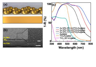
A team of Korean researchers, affiliated with UNIST [Ulsan National Institute of Science and Technology] has recently pioneered in developing a new type of multilayered (Au NPs/TiO2/Au) photoelectrode that boosts the ability of solar water-splitting to produce hydrogen. According to the research team, this special photoelectrode, inspired by the way plants convert sunlight into energy is capable of absorbing visible light from the sun, and then using it to split water molecules (H2O) into hydrogen and oxygen.

A Feb. 1, 2016 UNIST news release, which originated the news item, expands on the theme,

This multilayered photoelectrode takes the form of two-dimensional hybrid metal-dielectric structure, which mainly consists of three layers of gold (Au) film, ultrathin TiO2 layer (20 nm), and gold nanoparticles (Au NPs). In a study, reported in the January 21, 2016 issue of Nano Energy, the team reported that this promising photoelectrode shows high light absorption of about 90% in the visible range 380–700 nm, as well as significant enhancement in photo-catalytic applications.

The researchers have made an image illustrating their work available,

Two-dimensional metastructured film with Titanium Oxide is fabricated as a photo-catalytic photoanode with exceptional visible light absorption. Courtesy: UNIST

Two-dimensional metastructured film with Titanium Oxide is fabricated as a photo-catalytic photoanode with exceptional visible light absorption. Courtesy: UNIST

Back to the news release,

Many structural designs, such as hierarchical and branched assemblies of nanoscale materials have been suggested to increase the UV-visible absorption and to enhance water-splitting efficiency. However, through incorporation of plasmonic metal nanoparticles (i.e. Au) to TiO2 structures, their photoelectrodes have shown to enhance the photoactivity in the entire UV-visible region of solar spectrum when compared with the existing ones, the team reports.

Prof. Jeong Min Baik of UNIST (School of Materials Science and Engineering) states, “Several attemps have been made to use UV-based photoelectrodes for hydrogen production, but this is the first time to use the metal-dielectric hybrid-structured film with TiO2 for oxygen production.” Moreover, according to Prof. Baik, this special type of photoelectrode uses approximately 95% of the visible spectrum of sunlight, which makes up a substantial portion (40%) of full sunlight. He adds, “The developed technology is expected to improve hydrogen production efficiency.”

Prof. Heon Lee (Korean University) states, “This metal-dielectric hybrid-structured film is expected to further reduce the overall cost of producing hydrogen, as it doesn’t require complex operation processes.” He continues by saying, “Using nanoimprint lithography, mass production of hydrogen will be soon possible.”

Prof. Baik adds, “This simple system may serve as an efficient platform for solar energy conversion, utilizing the whole UV-visible range of solar spectrum based on two-dimensional plasmonic photoelectrodes.”

Here’s a link to and a citation for the paper,

Two-dimensional metal-dielectric hybrid-structured film with titanium oxide for enhanced visible light absorption and photo-catalytic application by Joonmo Park, Hee Jun Kim, SangHyeon Nam, Hyowook Kim, Hak-Jong Choi, Youn Jeong Jang, Jae Sung Lee, Jonghwa Shin, Heon Lee, Jeong Min Baik. Nano Energy Volume 21, March 2016, Pages 115–122 doi:10.1016/j.nanoen.2016.01.004

This paper is behind a paywall.

Parvus Therapeutics (Calgary, Canada) and reprogramming immune cells

An international collaboration of Canadian, Spanish, and US scientists has announced a new therapeutic approach which could reverse autoimmune diseases in a Feb. 17, 2016 news item on Nanotechnology Now,

• Nanotechnology Approach Restores Glucose Regulation and Motor Function in In Vivo Preclinical Models of Diabetes and Multiple Sclerosis, Respectively; Joint Swelling and Destruction Resolved in In Vivo Model of Rheumatoid Arthritis
• Parvus’ Approach Can Be Tailored to Treat Diverse Diseases

A Feb. 17, 2016 Parvus Therapeutics news release (also on EurekAlert), which originated the news item, provides more detail and a strong orientation to marketing communication,

Parvus Therapeutics today announced the publication in Nature of a seminal paper describing the discovery and applications of a novel therapeutic approach employing nanomedicines, referred to as “Navacims”TM, to reprogram white blood cells to become regulatory cells capable of blunting autoimmune responses and restoring the equilibrium of the immune system. Navacims are nanoparticles (NPs) coated with disease-relevant peptide-major histocompatibility complexes (pMHCs) that alter the behavior of pathogenic T lymphocytes by binding directly to their antigen receptors. The peer-reviewed article, titled “Expanding antigen-specific regulatory networks to treat autoimmunity” reports on a body of work, including results in multiple in vivo disease models, built on more than eight years of research by Parvus Founder and Chief Scientific Officer, Pere Santamaria, M.D., Ph.D.

Dr. Santamaria commented, “Autoimmune diseases, including type 1 diabetes, multiple sclerosis, and rheumatoid arthritis, are extraordinarily complex responses of our immune system against some of our own tissues (e.g. pancreas, brain and joints, respectively), leading to chronic organ inflammation, organ dysfunction, and, in some cases, premature death. Blunting these incompletely understood immune responses without suppressing the normal components of our immune system that protect us against infection and cancer is not currently possible.”

“However, our work offers a pharmaceutical solution to this fundamental problem,” Dr. Santamaria continued. “Navacims essentially re-program disease-causing white blood cells to become disease-suppressing cells, known as regulatory cells, leading to sustained therapeutic effects in various spontaneous and experimental autoimmune diseases, as reported in our article in Nature. Essentially, we have found that Navacims can be tailored to treat a wide range of autoimmune diseases, while sharing a common structure. Importantly, they have been shown to affect human white blood cells in the same manner as they do murine cells. Furthermore, Navacims have shown promising safety findings in preclinical in vivo models. Based on our results to date, we believe Navacims represent a therapeutic platform with broad-ranging health care implications.”

Findings being reported in Nature include:

pMHC class II Navacims expanded cognate CD4+ T-cells that consistently have a TR1-like, regulatory T cell surface phenotype, transcriptional pattern and cytokine profile (mouse=human TR1 cells) systemically.

pMHC class II-Navacims designed to target T cells in newly diabetic nonobese (NOD) mice restored normoglycemia (normal blood sugar regulation) in the majority of the mice tested.

Tailored pMHC class II Navacims restored motor function to paralyzed C57BL/6 mice at the peak of Experimental Autoimmune Encephalomyelitis (a model of Multiple Sclerosis).

pMHC class II Navacims, targeting disease-causing T cells in joints, resolved joint swelling and destruction in arthritic mice.

“The findings being reported in Nature represent a scientific advance for Parvus and also a major achievement in the field of Immunology,” said Janice M. LeCocq, CEO of Parvus. “We believe that Dr. Santamaria’s work has the potential to transform the treatment of many of the more than 80 major autoimmune diseases affecting humankind, alleviating the suffering of millions of patients and their families. Over the coming year, we will be dedicating much of our in-house efforts to the advancement of our two lead programs for type 1 diabetes and multiple sclerosis.”

“Dr. Santamaria’s work to target the immune system dysfunction that causes type 1 diabetes represents the kind of innovative work that JDRF believes will eventually get us to a cure for this disease,” said Juvenile Diabetes Research Foundation Vice President of Discovery Research Julia Greenstein, Ph.D. “He and his colleagues have made exciting progress towards possibly developing a new class of drugs that could rebalance certain T-cells and ultimately provide a cure for type 1 diabetes and other autoimmune diseases as well.” The JDRF has funded the work of Dr. Santamaria and his colleagues at Parvus to explore Navacim-based treatments for diabetes.

Parvus’ strategy is to establish partnerships with major pharmaceutical companies to undertake the clinical and commercial development of many of its product pipeline candidates while also reserving rights to others suitable for its own development and commercialization. Parvus currently is engaged in late stage discussions with multiple pharmaceutical companies with regard to the type 1 diabetes (T1D) program. Manufacturing scale-up is now underway to supply upcoming preclinical and clinical studies.

The work being reported in Nature was led by Dr. Pere Santamaria and largely executed at the University of Calgary, Cumming School of Medicine (animal models of disease) and the Institut d’Investigacions Biomèdiques August Pi i Sunyer (IDIBAPS) (humanized mouse work), with significant contributions from investigators at Institutions in Europe and the US. Further, Innovate Calgary, the technology-transfer and business-incubation center for the University of Calgary, provided early support for the transfer of the Navacims technology to and incubation of Parvus Therapeutics, which was organized as a separate entity in 2012.

It should be noted that this intervention has been tested on ‘humanized’ mice and, at this point, there don’t seem to have been any human clinical trials. At a guess I’d say we’re still several years away from this therapeutic intervention reaching the market, should it prove to be successful in humans.

Here’s a link to and a citation for the paper,

Expanding antigen-specific regulatory networks to treat autoimmunity by Xavier Clemente Casares, Jesus Blanco, Poornima Ambalavanan, Jun Yamanouchi, Santiswarup Singha, Cesar Fandos, Sue Tsai, Jinguo Wang, Nahir Garabatos, Cristina Izquierdo, Smriti Agrawal, Michael B. Keough, V. Wee Yong, Eddie James, Anna Moore, Yang Yang, Thomas Stratmann, Pau Serra, & Pere Santamaria. Nature (2016) doi:10.1038/nature16962 Published online 17 February 2016

This paper is behind a paywall.

Indian researchers establish a multiplex number to identify efficiency of multilevel resistive switching devices

There’s a Feb. 1, 2016 Nanowerk Spotlight article by Dr. Abhay Sagade of Cambridge University (UK) about defining efficiency in memristive devices,

In a recent study, researchers at the Jawaharlal Nehru Centre for Advanced Scientific Research (JNCASR), Bangalore, India, have defined a new figure-of-merit to identify the efficiency of resistive switching devices with multiple memory states. The research was carried out in collaboration with the Indian Institute of Technology Madras (IITM), Chennai, and financially supported by Department of Science and Technology, New Delhi.

The scientists identified the versatility of palladium oxide (PdO) as a novel resistive switching material for use in resistive memory devices. Due to the availability to switch multiple redox states in the PdO system, researchers have controlled it by applying different amplitudes of voltage pulses.

To date, many materials have shown multiple memory states but there have been no efforts to define the ability of the fabricated device to switch between all possible memory states.

In this present report, the authors have defined the efficacy in a term coined as “multiplex number (M)” to quantify the performance of a multiple memory switching device:

For the PdO MRS device with five memory states, the multiplex number is found to be 5.7, which translates to 70% efficiency in switching. This is the highest value of M observed in any multiple memory device.

As multilevel resistive switching devices are expected to have great significance in futuristic brain-like memory devices [neuromorphic engineering products], the definition of their efficiency will provide a boost to the field. The number M will assist researches as well as technologist in classifying and deciding the true merit of their memory devices.

Here’s a link to and a citation for the paper Sagade is discussing,

Defining Switching Efficiency of Multilevel Resistive Memory with PdO as an Example by K. D. M. Rao, Abhay A. Sagade, Robin John, T. Pradeep and G. U. Kulkarni. Advanced Electronic Materials Volume 2, Issue 2, February 2016 DOI: 10.1002/aelm.201500286

© 2016 WILEY-VCH Verlag GmbH & Co. KGaA, Weinheim

This article is behind a paywall.

Korean researchers fabricate cross-shaped memristors

I’ve been a bit late getting this Korean research concerning memristors into a posting. A Jan. 30, 2016 news item on Nanotechnology Now announces a new means of fabricating memristors,

Along with the fast development of modern information technology, charge-based memories, such as DRAM and flash memory, are being aggressively scaled down to meet the current trend of small size devices. A memory device with high density, faster speed, and low power consumption is desired to satisfy Moore’s law in the next few decades. Among the candidates of next-generation memory devices, cross-bar-shaped non-volatile resistive memory (memristor) is one of the most attractive solutions for its non-volatility, faster access speed, ultra-high density and easier fabrication process.

Conventional memristors are usually fabricated through conventional optical, imprint, and e-beam lithographic approaches. However, to meet Moore’s law, the assembly of memristors comprised of 1-dimensional (1D) nanowires must be demonstrated to achieve cell dimensions beyond limit of state-of-art lithographic techniques, thus allowing one to fully exploit the scaling potential of high density memory array.

Prof. Tae-Woo Lee (Dept. of Materials Science and Engineering) and his research team have developed a rapid printing technology for high density and scalable memristor array composed of cross-bar-shaped metal nanowires. The research team, which consists of Prof. Tae-Woo Lee, research professor Wentao Xu, and doctoral student Yeongjun Lee at POSTECH [Pohang University of Science and Technology], Korea, published their findings in Advanced Materials.

A Jan. 28, 2016 POSTECH news release, which originated the news item, expands on the theme,

They applied an emerging technique, electrohydrohynamic nanowire printing (e-NW printing), which directly prints highly-aligned nanowire array on a large scale into the fabrication of microminiature memristors, with cross-bar-shaped conductive Cu nanowires jointed with a nanometer-scale CuxO layer. The metal-oxide-metal structure resistive memory device exhibited excellent electrical performance with reproducible resistive switching behavior.

This simple and fast fabrication process avoids conventional vacuum techniques to significantly reduce the industrial-production cost and time. This method paved the way to the future down-scaling of electronic circuits, since 1D conductors represent a logical way to extreme scaling of data processing devices in the single-digit nanometer scale.

They also succeeded in printing memristor array with various shapes, such as parallel lines with adjustable pitch, grids, and waves which can offer a future stretchable memory for integration into textile to serve as a basic building block for smart fabrics and wearable electronics.

“This technology reduces lead time and cost remarkably compared with existing manufacturing methods of cross-bar-shaped nanowire memory and simplifies its method of construction,” said Prof. Lee. “In particular, this technology will be used as a source technology to realize smart fabric, wearable computers, and textile electronic devices.”

Here’s a link to and a citation for the paper,

[Nanowires:] Simple, Inexpensive, and Rapid Approach to Fabricate Cross-Shaped Memristors Using an Inorganic-Nanowire-Digital-Alignment Technique and a One-Step Reduction Process by Wentao Xu, Yeongjun Lee, Sung-Yong Min, Cheolmin Park, andTae-Woo Lee. Advanced Materials Volume 28, Issue 3 January 20, 2016 Page 591  DOI: 10.1002/adma.201503153 Article first published online: 20 NOV 2015

© 2015 WILEY-VCH Verlag GmbH & Co. KGaA, Weinheim

This paper is behind a paywall.