Tag Archives: 2D materials

Canadian and Italian researchers go beyond graphene with 2D polymers

According to a May 20,2020 McGill University news release (also on EurkekAltert), a team of Canadian and Italian researchers has broken new ground in materials science (Note: There’s a press release I found a bit more accessible and therefore informative coming up after this one),

A study by a team of researchers from Canada and Italy recently published in Nature Materials could usher in a revolutionary development in materials science, leading to big changes in the way companies create modern electronics.

The goal was to develop two-dimensional materials, which are a single atomic layer thick, with added functionality to extend the revolutionary developments in materials science that started with the discovery of graphene in 2004.

In total, 19 authors worked on this paper from INRS [Institut National de la Recherche Scientifique], McGill {University], Lakehead [University], and Consiglio Nazionale delle Ricerche, the national research council in Italy.

This work opens exciting new directions, both theoretical and experimental. The integration of this system into a device (e.g. transistors) may lead to outstanding performances. In addition, these results will foster more studies on a wide range of two-dimensional conjugated polymers with different lattice symmetries, thereby gaining further insights into the structure vs. properties of these systems.

The Italian/Canadian team demonstrated the synthesis of large-scale two-dimensional conjugated polymers, also thoroughly characterizing their electronic properties. They achieved success by combining the complementary expertise of organic chemists and surface scientists.

“This work represents an exciting development in the realization of functional two-dimensional materials beyond graphene,” said Mark Gallagher, a Physics professor at Lakehead University.

“I found it particularly rewarding to participate in this collaboration, which allowed us to combine our expertise in organic chemistry, condensed matter physics, and materials science to achieve our goals.”

Dmytro Perepichka, a professor and chair of Chemistry at McGill University, said they have been working on this research for a long time.

“Structurally reconfigurable two-dimensional conjugated polymers can give a new breadth to applications of two-dimensional materials in electronics,” Perepichka said.

“We started dreaming of them more than 15 years ago. It’s only through this four-way collaboration, across the country and between the continents, that this dream has become the reality.”

Federico Rosei, a professor at the Énergie Matériaux Télécommunications Research Centre of the Institut National de la Recherche Scientifique (INRS) in Varennes who holds the Canada Research Chair in Nanostructured Materials since 2016, said they are excited about the results of this collaboration.

“These results provide new insights into mechanisms of surface reactions at a fundamental level and simultaneously yield a novel material with outstanding properties, whose existence had only been predicted theoretically until now,” he said.

About this study

Synthesis of mesoscale ordered two-dimensional π-conjugated polymers with semiconducting properties” by G. Galeotti et al. was published in Nature Materials.

This research was partially supported by a project Grande Rilevanza Italy-Quebec of the Italian Ministero degli Affari Esteri e della Cooperazione Internazionale, Direzione Generale per la Promozione del Sistema Paese, the Natural Sciences and Engineering Research Council of Canada, the Fonds Québécois de la recherche sur la nature et les technologies and a US Army Research Office. Federico Rosei is also grateful to the Canada Research Chairs program for funding and partial salary support.

About McGill University

Founded in Montreal, Quebec, in 1821, McGill is a leading Canadian post-secondary institution. It has two campuses, 11 faculties, 13 professional schools, 300 programs of study and over 40,000 students, including more than 10,200 graduate students. McGill attracts students from over 150 countries around the world, its 12,800 international students making up 31% per cent of the student body. Over half of McGill students claim a first language other than English, including approximately 19% of our students who say French is their mother tongue.

About the INRS
The Institut National de la Recherche Scientifique (INRS) is the only institution in Québec dedicated exclusively to graduate level university research and training. The impacts of its faculty and students are felt around the world. INRS proudly contributes to societal progress in partnership with industry and community stakeholders, both through its discoveries and by training new researchers and technicians to deliver scientific, social, and technological breakthroughs in the future.

Lakehead University
Lakehead University is a fully comprehensive university with approximately 9,700 full-time equivalent students and over 2,000 faculty and staff at two campuses in Orillia and Thunder Bay, Ontario. Lakehead has 10 faculties, including Business Administration, Education, Engineering, Graduate Studies, Health & Behavioural Sciences, Law, Natural Resources Management, the Northern Ontario School of Medicine, Science & Environmental Studies, and Social Sciences & Humanities. In 2019, Maclean’s 2020 University Rankings, once again, included Lakehead University among Canada’s Top 10 primarily undergraduate universities, while Research Infosource named Lakehead ‘Research University of the Year’ in its category for the fifth consecutive year. Visit www.lakeheadu.ca

I’m a little surprised there wasn’t a quote from one of the Italian researchers in the McGill news release but then there isn’t a quote in this slightly more accessible May 18, 2020 Consiglio Nazionale delle Ricerche press release either,

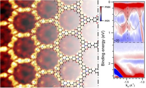
Graphene’s isolation took the world by surprise and was meant to revolutionize modern electronics. However, it was soon realized that its intrinsic properties limit the utilization in our daily electronic devices. When a concept of Mathematics, namely Topology, met the field of on-surface chemistry, new materials with exotic features were theoretically discovered. Topological materials exhibit technological relevant properties such as quantum hall conductivity that are protected by a concept similar to the comparison of a coffee mug and a donut.  These structures can be synthesized by the versatile molecular engineering toolbox that surface reactions provide. Nevertheless, the realization of such a material yields access to properties that suit the figure of merits for modern electronic application and could eventually for example lead to solve the ever-increasing heat conflict in chip design. However, problems such as low crystallinity and defect rich structures prevented the experimental observation and kept it for more than a decade a playground only investigated theoretically.

An international team of scientists from Institut National de la Recherche Scientifique (Centre Energie, Matériaux et Télécommunications), McGill University and Lakehead University, both located in Canada, and the SAMOS laboratory of the Istituto di Struttura della Materia (Cnr), led by Giorgio Contini, demonstrates, in a recent publication on Nature Materials, that the synthesis of two-dimensional π-conjugated polymers with topological Dirac cone and flats bands became a reality allowing a sneak peek into the world of organic topological materials.

Complementary work of organic chemists and surface scientists lead to two-dimensional polymers on a mesoscopic scale and granted access to their electronic properties. The band structure of the topological polymer reveals both flat bands and a Dirac cone confirming the prediction of theory. The observed coexistence of both structures is of particular interest, since whereas Dirac cones yield massless charge carriers (a band velocity of the same order of magnitude of graphene has been obtained), necessary for technological applications, flat bands quench the kinetic energy of charge carriers and could give rise to intriguing phenomena such as the anomalous Hall effect, surface superconductivity or superfluid transport.

This work paths multiple new roads – both theoretical and experimental nature. The integration of this topological polymer into a device such as transistors possibly reveals immense performance. On the other hand, it will foster many researchers to explore a wide range of two-dimensional polymers with different lattice symmetries, obtaining insight into the relationship between geometrical and electrical topology, which would in return be beneficial to fine tune a-priori theoretical studies. These materials – beyond graphene – could be then used for both their intrinsic properties as well as their interplay in new heterostructure designs.

The authors are currently exploring the practical use of the realized material trying to integrate it into transistors, pushing toward a complete designing of artificial topological lattices.

This work was partially supported by a project Grande Rilevanza Italy-Quebec of the Italian Ministero degli Affari Esteri e della Cooperazione Internazionale (MAECI), Direzione Generale per la Promozione del Sistema Paese.

The Italians also included an image to accompany their press release,

Image of the synthesized material and its band structure Courtesy: Consiglio Nazionale delle Ricerche

My heart sank when I saw the number of authors for this paper (WordPress no longer [since their Christmas 2018 update] makes it easy to add the author’s names quickly to the ‘tags field’). Regardless and in keeping with my practice, here’s a link to and a citation for the paper,

Synthesis of mesoscale ordered two-dimensional π-conjugated polymers with semiconducting properties by G. Galeotti, F. De Marchi, E. Hamzehpoor, O. MacLean, M. Rajeswara Rao, Y. Chen, L. V. Besteiro, D. Dettmann, L. Ferrari, F. Frezza, P. M. Sheverdyaeva, R. Liu, A. K. Kundu, P. Moras, M. Ebrahimi, M. C. Gallagher, F. Rosei, D. F. Perepichka & G. Contini. Nature Materials (2020) DOI: https://doi.org/10.1038/s41563-020-0682-z Published 18 May 2020

This paper is behind a paywall.

Borophene and next generation electronics?

2D materials as signified by the ‘ene’ suffix are, as far as I can tell, always associated with electronics—initially. Borophene is not an exception.

This borophene news was announced in a December 3, 2018 news item on ScienceDaily,

Borophene — two-dimensional (2-D) atom-thin-sheets of boron, a chemical element traditionally found in fiberglass insulation — is anything but boring. Though boron is a nonmetallic semiconductor in its bulk (3-D) form, it becomes a metallic conductor in 2-D. Borophene is extremely flexible, strong, and lightweight — even more so than its carbon-based analogue, graphene. [Providing a little competition to the Europeans who are seriously pursuing nanotechnology-enabled electronics and other applications with graphene?] These unique electronic and mechanical properties make borophene a promising material platform for next-generation electronic devices such as wearables, biomolecule sensors, light detectors, and quantum computers.

Now, physicists from the U.S. Department of Energy’s (DOE) Brookhaven National Laboratory and Yale University have synthesized borophene on copper substrates with large-area (ranging in size from 10 to 100 micrometers) single-crystal domains (for reference, a strand of human hair is about 100 micrometers wide). Previously, only nanometer-size single-crystal flakes of borophene had been produced. The advance, reported on Dec. 3 [2018] in Nature Nanotechnology, represents an important step in making practical borophene-based devices possible.

A December 3, 2018 Brookhaven National Laboratory (BNL) news release (also on EurekAlert), which originated the news item, provides more detail about 2D materials and the specifics of this borophene research,

For electronic applications, high-quality single crystals–periodic arrangements of atoms that continue throughout the entire crystal lattice without boundaries or defects–must be distributed over large areas of the surface material (substrate) on which they are grown. For example, today’s microchips use single crystals of silicon and other semiconductors. Device fabrication also requires an understanding of how different substrates and growth conditions impact a material’s crystal structure, which determines its properties.

“We increased the size of the single-crystal domains by a factor of a million,” said co-author and project lead Ivan Bozovic, senior scientist and Molecular Beam Epitaxy Group Leader in Brookhaven Lab’s Condensed Matter Physics and Materials Science (CMPMS) Department and adjunct professor of applied physics at Yale University. “Large domains are required to fabricate next-generation electronic devices with high electron mobility. Electrons that can easily and quickly move through a crystal structure are key to improving device performance.”

A new 2-D material

Since the 2004 discovery of graphene–a single sheet of carbon atoms, which can be peeled from graphite, the core component of pencils, with Scotch tape–scientists have been on the hunt for other 2-D materials with remarkable properties. The chemical bonds between carbon atoms that impart graphene with its strength make manipulating its structure difficult.

Theorists predicted that boron (next to carbon on the Periodic Table, with one less electron) deposited on an appropriately chosen substrate could form a 2-D material similar to graphene. But this prediction was not experimentally confirmed until three years ago, when scientists synthesized borophene for the very first time. They deposited boron onto silver substrates under ultrahigh-vacuum conditions through molecular beam epitaxy (MBE), a precisely controlled atomic layer-by-layer crystal growth technique. Soon thereafter, another group of scientists grew borophene on silver, but they proposed an entirely different crystal structure.

“Borophene is structurally similar to graphene, with a hexagonal network made of boron (instead of carbon) atoms on each of the six vertices defining the hexagon,” said Bozovic. “However, borophene is different in that it periodically has an extra boron atom in the center of the hexagon. The crystal structure tends to be theoretically stable when about four out of every five center positions are occupied and one is vacant.”

According to theory, while the number of vacancies is fixed, their arrangement is not. As long as the vacancies are distributed in a way that maintains the most stable (lowest energy) structure, they can be rearranged. Because of this flexibility, borophene can have multiple configurations.

A small step toward device fabrication

In this study, the scientists first investigated the real-time growth of borophene on silver surfaces at various temperatures. They grew the samples at Yale in an ultra-high vacuum low-energy electron microscope (LEEM) equipped with an MBE system. During and after the growth process, they bombarded the sample with a beam of electrons at low energy and analyzed the low-energy electron diffraction (LEED) patterns produced as electrons were reflected from the crystal surface and projected onto a detector. Because the electrons have low energy, they can only reach the first few atomic layers of the material. The distance between the reflected electrons (“spots” in the diffraction patterns) is related to the distance between atoms on the surface, and from this information, scientists can reconstruct the crystal structure.

In this case, the patterns revealed that the single-crystal borophene domains were only tens of nanometers in size–too small for fabricating devices and studying fundamental physical properties–for all growth conditions. They also resolved the controversy about borophene’s structure: both structures exist, but they form at different temperatures. The scientists confirmed their LEEM and LEED results through atomic force microscopy (AFM). In AFM, a sharp tip is scanned over a surface, and the measured force between the tip and atoms on the surface is used to map the atomic arrangement.

To promote the formation of larger crystals, the scientists then switched the substrate from silver to copper, applying the same LEEM, LEED, and AFM techniques. Brookhaven scientists Percy Zahl and Ilya Drozdov also imaged the surface structure at high resolution using a custom-built scanning tunneling microscope (STM) with a carbon monoxide probe tip at Brookhaven’s Center for Functional Nanomaterials (CFN)–a U.S. Department of Energy (DOE) Office of Science User Facility. Yale theorists Stephen Eltinge and Sohrab Ismail-Beigi performed calculations to determine the stability of the experimentally obtained structures. After identifying which structures were most stable, they simulated the electron diffraction spectra and STM images and compared them to the experimental data. This iterative process continued until theory and experiment were in agreement.

“From theoretical insights, we expected copper to produce larger single crystals because it interacts more strongly with borophene than silver,” said Bozovic. “Copper donates some electrons to stabilize borophene, but the materials do not interact too much as to form a compound. Not only are the single crystals larger, but the structures of borophene on copper are different from any of those grown on silver.”

Because there are several possible distributions of vacancies on the surface, various crystal structures of borophene can emerge. This study also showed how the structure of borophene can be modified by changing the substrate and, in some cases, the temperature or deposition rate.

The next step is to transfer the borophene sheets from the metallic copper surfaces to insulating device-compatible substrates. Then, scientists will be able to accurately measure resistivity and other electrical properties important to device functionality. Bozovic is particularly excited to test whether borophene can be made superconducting. Some theorists have speculated that its unusual electronic structure may even open a path to lossless transmission of electricity at room temperature, as opposed to the ultracold temperatures usually required for superconductivity. Ultimately, the goal in 2-D materials research is to be able to fine-tune the properties of these materials to suit particular applications.

Here’s a link to and a citation for the paper,

Large-area single-crystal sheets of borophene on Cu(111) surfaces by Rongting Wu, Ilya K. Drozdov, Stephen Eltinge, Percy Zahl, Sohrab Ismail-Beigi, Ivan Božović & Adrian Gozar. Nature Nanotechnology (2018) DOI: https://doi.org/10.1038/s41565-018-0317-6Published 03 December 2018

This paper is behind a paywall.

Two-dimensional arsenic (arsenene) for electronics

Another day, another ‘ene’ (e.g., graphene, borene, germanene, etc.). This ‘ene’ is arsenene, from an October 15, 2018 Wiley (Publications) news release (also on EurekAlert),

The discovery of graphene, a material made of one or very few atomic layers of carbon, started a boom. Today, such two-dimensional materials are no longer limited to carbon and are hot prospects for many applications, especially in microelectronics. In the journal Angewandte Chemie, scientists have now introduced a new 2D material: they successfully modified arsenene (arsenic in a graphene-like structure) with chloromethylene groups.

Two-dimensional materials are crystalline materials made of just a single or very few layers of atoms that often display unusual properties. However, the use of graphene for applications such as transistors is limited because it behaves more like a conductor than a semiconductor. Modified graphene and 2D materials based on other chemical elements with semiconducting properties have now been developed. One such material is β-arsenene, a two-dimensional arsenic in a buckled honeycomb structure derived from gray arsenic. Researchers hope that modification of this previously seldom-studied material could improve its semiconducting properties and lead the way to new applications in fields such as sensing, catalysis, optoelectronics, and other semiconductor technologies.

A team at the University of Chemistry and Technology Prague (Czech Republic) and Nanyang Technical University (Singapore), led by Zdenek Sofer and Martin Pumera has now successfully produced a highly promising covalent modification of β-arsenene.

The arsenene was produced by milling gray arsenic in tetrahydrofuran. The shear forces cause two-dimensional layers to split off and disperse into the solvent. The researchers then introduce dichloromethane and add an organic lithium compound (butyllithium). These two reagents form an intermediate called chlorocarbene, a molecule made of one carbon atom, one hydrogen atom, and one chlorine atom. The carbon atom is short two bonding partners, a state that makes the whole class of carbene molecules highly reactive. Arsenene contains free electron pairs that “stick out” from the surface and can easily enter into bonds to chlorocarbene.

This approach leads to high coverage of the arsenene surface with chloromethylene groups, as confirmed by a variety of analysis methods (X-ray photoelectron spectroscopy, FT-IR spectroscopy, elemental analysis by transmission electron microscopy). The modified arsenene is more stable than pure arsenene and exhibits strong luminescence and electronic properties that make it attractive for optoelectronic applications. In addition, the chloromethylene units could serve as a starting point for further interesting modifications.

As always with an ‘ene’, the major focus is on electronics. Here’s a link to and a citation for the paper,

Covalent Functionalization of Exfoliated Arsenic with Chlorocarbene by Jiri Sturala, Adriano Ambrosi, Zdeněk Sofer, Martin Pumera. Angewandte Chimie International Edition Volume 57, Issue 45 November 5, 2018 Pages 14837-14840 DOI: https://doi.org/10.1002/anie.201809341 First published: 31 August 2018

This paper is behind a paywall.

The brittleness of molybdenum diselenide

With the finding that molybdenum diselenide is not as strong as previously believed, industry may want to reconsider 2D materials before incorporating them in new products according to a Rice University (Texas, US) scientist. From a Nov. 14, 2016 news item on Nanowerk,

Scientists at Rice University have discovered that an atom-thick material being eyed for flexible electronics and next-generation optical devices is more brittle than they expected.

The Rice team led by materials scientist Jun Lou tested the tensile strength of two-dimensional, semiconducting molybdenum diselenide and discovered that flaws as small as one missing atom can initiate catastrophic cracking under strain.

The finding may cause industry to look more carefully at the properties of 2-D materials before incorporating them in new technologies, he said.


A Nov. 14, 2016 Rice University news release (also on EurekAlert), which originated the news item, provides more insight into the research,

“It turns out not all 2-D crystals are equal,” said Lou, a Rice professor of materials science and nanoengineering. “Graphene is a lot more robust compared with some of the others we’re dealing with right now, like this molybdenum diselenide. We think it has something to do with defects inherent to these materials.”

The defects could be as small as a single atom that leaves a vacancy in the crystalline structure, he said. “It’s very hard to detect them,” he said. “Even if a cluster of vacancies makes a bigger hole, it’s difficult to find using any technique. It might be possible to see them with a transmission electron microscope, but that would be so labor-intensive that it wouldn’t be useful.”

Molybdenum diselenide is a dichalcogenide, a two-dimensional semiconducting material that appears as a graphene-like hexagonal array from above but is actually a sandwich of metallic atoms between two layers of chalcogen atoms, in this case, selenium. Molybdenum diselenide is being considered for use as transistors and in next-generation solar cells, photodetectors and catalysts as well as electronic and optical devices.

Lou and colleagues measured the material’s elastic modulus, the amount of stretching a material can handle and still return to its initial state, at 177.2 (plus or minus 9.3) gigapascals. Graphene is more than five times as elastic. They attributed the large variation to pre-existing flaws of between 3.6 and 77.5 nanometers.

Its fracture strength, the amount of stretching a material can handle before breaking, was measured at 4.8 (plus or minus 2.9) gigapascals. Graphene is nearly 25 times stronger.

Part of the project led by Rice postdoctoral researcher Yingchao Yang required moving molybdenum diselenide from a growth chamber in a chemical vapor deposition furnace to a microscope without introducing more defects. Yang solved the problem using a dry transfer process in place of a standard acid washing that would have ruined the samples.

To test samples, Yang placed rectangles of molybdenum diselenide onto a sensitive electron microscope platform invented by the Lou group. Natural van der Waals forces held the samples in place on springy cantilever arms that measured the applied stress.

Lou said the group attempted to measure the material’s fracture toughness, an indicator of how likely cracks are to propagate, as they had in an earlier study on graphene. But they found that pre-cutting cracks into molybdenum diselenide resulted in it shattering before stress could be applied, he said.

“The important message of this work is the brittle nature of these materials,” Lou said. “A lot of people are thinking about using 2-D crystals because they’re inherently thin. They’re thinking about flexible electronics because they are semiconductors and their theoretical elastic strength should be very high. According to our calculations, they can be stretched up to 10 percent.

“But in reality, because of the inherent defects, you rarely can achieve that much strength. The samples we have tested so far broke at 2 to 3 percent (of the theoretical maximum) at most,” Lou said. “That should still be fine for most flexible applications, but unless they find a way to quench the defects, it will be very hard to achieve the theoretical limits.”


When seen from above, the atoms in two-dimensional molybdenum diselenide resemble a hexagonal grid, like graphene. But in reality, the darker molybdenum atoms are sandwiched between top and bottom layers of selenide atoms. Rice University researchers tested the material for its tensile strength. Courtesy of the Lou Group

When seen from above, the atoms in two-dimensional molybdenum diselenide resemble a hexagonal grid, like graphene. But in reality, the darker molybdenum atoms are sandwiched between top and bottom layers of selenide atoms. Rice University researchers tested the material for its tensile strength. Courtesy of the Lou Group

Here’s a link to and a citation for the paper,


Brittle Fracture of 2D MoSe2 by Yingchao Yang, Xing Li, Minru Wen, Emily Hacopian, Weibing Chen, Yongji Gong, Jing Zhang, Bo Li, Wu Zhou, Pulickel M. Ajayan, Qing Chen, Ting Zhu, and Jun Lou. Advanced Materials DOI: 10.1002/adma.201604201 Version of Record online: 3 NOV 2016

© 2016 WILEY-VCH Verlag GmbH & Co. KGaA, Weinheim

This paper is behind a paywall.

Replace silicon with black phosphorus instead of graphene?

I have two black phosphorus pieces. This first piece of research comes out of ‘La belle province’ or, as it’s more usually called, Québec (Canada).

Foundational research on phosphorene

There’s a lot of interest in replacing silicon for a number of reasons and, increasingly, there’s interest in finding an alternative to graphene.

A July 7, 2015 news item on Nanotechnology Now describes a new material for use as transistors,

As scientists continue to hunt for a material that will make it possible to pack more transistors on a chip, new research from McGill University and Université de Montréal adds to evidence that black phosphorus could emerge as a strong candidate.

In a study published today in Nature Communications, the researchers report that when electrons move in a phosphorus transistor, they do so only in two dimensions. The finding suggests that black phosphorus could help engineers surmount one of the big challenges for future electronics: designing energy-efficient transistors.

A July 7, 2015 McGill University news release on EurekAlert, which originated the news item, describes the field of 2D materials and the research into black phosphorus and its 2D version, phosperene (analogous to graphite and graphene),

“Transistors work more efficiently when they are thin, with electrons moving in only two dimensions,” says Thomas Szkopek, an associate professor in McGill’s Department of Electrical and Computer Engineering and senior author of the new study. “Nothing gets thinner than a single layer of atoms.”

In 2004, physicists at the University of Manchester in the U.K. first isolated and explored the remarkable properties of graphene — a one-atom-thick layer of carbon. Since then scientists have rushed to to investigate a range of other two-dimensional materials. One of those is black phosphorus, a form of phosphorus that is similar to graphite and can be separated easily into single atomic layers, known as phosphorene.

Phosphorene has sparked growing interest because it overcomes many of the challenges of using graphene in electronics. Unlike graphene, which acts like a metal, black phosphorus is a natural semiconductor: it can be readily switched on and off.

“To lower the operating voltage of transistors, and thereby reduce the heat they generate, we have to get closer and closer to designing the transistor at the atomic level,” Szkopek says. “The toolbox of the future for transistor designers will require a variety of atomic-layered materials: an ideal semiconductor, an ideal metal, and an ideal dielectric. All three components must be optimized for a well designed transistor. Black phosphorus fills the semiconducting-material role.”

The work resulted from a multidisciplinary collaboration among Szkopek’s nanoelectronics research group, the nanoscience lab of McGill Physics Prof. Guillaume Gervais, and the nanostructures research group of Prof. Richard Martel in Université de Montréal’s Department of Chemistry.

To examine how the electrons move in a phosphorus transistor, the researchers observed them under the influence of a magnetic field in experiments performed at the National High Magnetic Field Laboratory in Tallahassee, FL, the largest and highest-powered magnet laboratory in the world. This research “provides important insights into the fundamental physics that dictate the behavior of black phosphorus,” says Tim Murphy, DC Field Facility Director at the Florida facility.

“What’s surprising in these results is that the electrons are able to be pulled into a sheet of charge which is two-dimensional, even though they occupy a volume that is several atomic layers in thickness,” Szkopek says. That finding is significant because it could potentially facilitate manufacturing the material — though at this point “no one knows how to manufacture this material on a large scale.”

“There is a great emerging interest around the world in black phosphorus,” Szkopek says. “We are still a long way from seeing atomic layer transistors in a commercial product, but we have now moved one step closer.”

Here’s a link to and a citation for the paper,

Two-dimensional magnetotransport in a black phosphorus naked quantum well by V. Tayari, N. Hemsworth, I. Fakih, A. Favron, E. Gaufrès, G. Gervais, R. Martel & T. Szkopek. Nature Communications 6, Article number: 7702 doi:10.1038/ncomms8702 Published 07 July 2015

This is an open access paper.

The second piece of research into black phosphorus is courtesy of an international collaboration.

A phosporene transistor

A July 9, 2015 Technical University of Munich (TUM) press release (also on EurekAlert) describes the formation of a phosphorene transistor made possible by the introduction of arsenic,

Chemists at the Technische Universität München (TUM) have now developed a semiconducting material in which individual phosphorus atoms are replaced by arsenic. In a collaborative international effort, American colleagues have built the first field-effect transistors from the new material.

For many decades silicon has formed the basis of modern electronics. To date silicon technology could provide ever tinier transistors for smaller and smaller devices. But the size of silicon transistors is reaching its physical limit. Also, consumers would like to have flexible devices, devices that can be incorporated into clothing and the likes. However, silicon is hard and brittle. All this has triggered a race for new materials that might one day replace silicon.

Black arsenic phosphorus might be such a material. Like graphene, which consists of a single layer of carbon atoms, it forms extremely thin layers. The array of possible applications ranges from transistors and sensors to mechanically flexible semiconductor devices. Unlike graphene, whose electronic properties are similar to those of metals, black arsenic phosphorus behaves like a semiconductor.

The press release goes on to provide more detail about the collaboration and the research,

A cooperation between the Technical University of Munich and the University of Regensburg on the German side and the University of Southern California (USC) and Yale University in the United States has now, for the first time, produced a field effect transistor made of black arsenic phosphorus. The compounds were synthesized by Marianne Koepf at the laboratory of the research group for Synthesis and Characterization of Innovative Materials at the TUM. The field effect transistors were built and characterized by a group headed by Professor Zhou and Dr. Liu at the Department of Electrical Engineering at USC.

The new technology developed at TUM allows the synthesis of black arsenic phosphorus without high pressure. This requires less energy and is cheaper. The gap between valence and conduction bands can be precisely controlled by adjusting the arsenic concentration. “This allows us to produce materials with previously unattainable electronic and optical properties in an energy window that was hitherto inaccessible,” says Professor Tom Nilges, head of the research group for Synthesis and Characterization of Innovative Materials.

Detectors for infrared

With an arsenic concentration of 83 percent the material exhibits an extremely small band gap of only 0.15 electron volts, making it predestined for sensors which can detect long wavelength infrared radiation. LiDAR (Light Detection and Ranging) sensors operate in this wavelength range, for example. They are used, among other things, as distance sensors in automobiles. Another application is the measurement of dust particles and trace gases in environmental monitoring.

A further interesting aspect of these new, two-dimensional semiconductors is their anisotropic electronic and optical behavior. The material exhibits different characteristics along the x- and y-axes in the same plane. To produce graphene like films the material can be peeled off in ultra thin layers. The thinnest films obtained so far are only two atomic layers thick.

Here’s a link to and a citation for the paper,

Black Arsenic–Phosphorus: Layered Anisotropic Infrared Semiconductors with Highly Tunable Compositions and Properties by Bilu Liu, Marianne Köpf, Ahmad N. Abbas, Xiaomu Wang, Qiushi Guo, Yichen Jia, Fengnian Xia, Richard Weihrich, Frederik Bachhuber, Florian Pielnhofer, Han Wang, Rohan Dhall, Stephen B. Cronin, Mingyuan Ge1 Xin Fang, Tom Nilges, and Chongwu Zhou. DOI: 10.1002/adma.201501758 Article first published online: 25 JUN 2015

© 2015 WILEY-VCH Verlag GmbH & Co. KGaA, Weinheim

This paper is behind a paywall.

Dexter Johnson, on his Nanoclast blog (on the Institute for Electrical and Electronics Engineers website), adds more information about black phosphorus and its electrical properties in his July 9, 2015 posting about the Germany/US collaboration (Note: Links have been removed),

Black phosphorus has been around for about 100 years, but recently it has been synthesized as a two-dimensional material—dubbed phosphorene in reference to its two-dimensional cousin, graphene. Black phosphorus is quite attractive for electronic applications like field-effect transistors because of its inherent band gap and it is one of the few 2-D materials to be a natively p-type semiconductor.

One final comment, I notice the Germany-US work was published weeks prior to the Canadian research suggesting that the TUM July 9, 2015 press release is an attempt to capitalize on the interest generated by the Canadian research. That’s a smart move.

Bringing the Nanoworld Together Workshop in Beijing, China, Sept. 24 – 25, 2014

The speakers currently confirmed for the ‘Bringing the Nanoworld Together Workshop organized by Oxford Instruments are from the UK, China, Canada, the US, and the Netherlands as per a July 2, 2014 news item on Nanowerk (Note: A link has been removed),

‘Bringing the Nanoworld Together’ is an event organised by Oxford Instruments to share the expertise of scientists in the field of Nanotechnology. It will be hosted at the IOS-CAS [Institute of Semiconductors-Chinese Academy of Sciences] Beijing.

Starting with half day plenary sessions on 2D materials with guest plenary speaker Dr Aravind Vijayaraghavan from the National Graphene Institute in Manchester, UK, and on Quantum Information Processing with guest plenary speaker Prof David Cory from the Institute for Quantum Computing, University of Waterloo, Canada, Oxford Instruments’ seminar at the IOP in Beijing from 24-25th September [2014] promises to discuss cutting edge nanotechnology solutions for multiple applications.

A July 1, 2014 Oxford Instruments press release, which originated the news item, describes the sessions and provides more details about the speakers,

Two parallel sessions will focus on thin film processing, & materials characterisation, surface science and cryogenic environments and a wide range of topics will be covered within each technical area. These sessions will include guest international and Chinese speakers from renowned research institutions, speakers from the host institute, and technical experts from Oxford Instruments. This will also present an excellent opportunity for networking between all participants.

Confirmed speakers include the following, but more will be announced soon:

Dr. Aravind Vijayaraghavan, National Graphene Institute, Manchester, UK
Prof David Cory, Institute for Quantum Computing, University of Waterloo, Canada
Prof Guoxing Miao, Institute for Quantum Computing, University of Waterloo, Canada
Prof. HE Ke, Tsinghua University, Institute of Physics, CAS, China
Dr. WANG Xiaodong, Institute of Semiconductors, CAS, China
Prof Erwin Kessels, Tue Eindhoven, Netherlands
Prof. ZENG Yi, Institute of Semiconductor, CAS, China
Prof Robert Klie, University of Illinois Chicago, USA
Prof. Xinran WANG, Nanjing University, China
Prof. Zhihai CHENG, National Centre for Nanoscience and Technology, China
Prof. Yeliang WANG, Institute of Physics, CAS, China

The thin film processing sessions will review latest etch and deposition technological advances, including: ALD, Magnetron Sputtering, ICP PECVD, Nanoscale Etch, MEMS, MBE and more.

Materials characterisation, Surface Science and Cryogenic Environment sessions will cover multiple topics and technologies including: Ultra high vacuum SPM, Cryo free low temperature solutions, XPS/ESCA, an introduction to atomic force microscopy (AFM) and applications such as nanomechanics, In-situ heating and tensile characterisation using EBSD, Measuring Layer thicknesses and compositions using EDS, Nanomanipulation and fabrication within the SEM / FIB.

The host of last year’s Nanotechnology Tools seminar in India, Prof. Rudra Pratap, Chairperson at the Centre for Nano Science and Engineering, Indian Institute of Science, IISC Bangalore commented, “This seminar has been extremely well organised with competent speakers covering a variety of processes and tools for nanofabrication. It is great to have practitioners of the art give talks and provide tips and solutions based on their experience, something that cannot be found in text books.”

“This workshop is a great opportunity for a wide range of scientists in research and manufacturing to discover practical aspects of many new and established processes, technologies and applications, directly from renowned scientists and a leading manufacturer with over 50 years in the industry”, comments Mark Sefton, Sector Head of Oxford Instruments NanoSolutions, “Delegates appreciate the informal workshop atmosphere of these events, encouraging delegates to participate through open discussion and sharing their questions and experiences.”

This seminar is free of charge but prior booking is essential.

You can register on the Oxford Instruments website’s Bringing the Nanoworld Together Workshop webpage,