This work on brainlike (neuromorphic) computing was announced in a June 30, 2022 Compuscript Ltd news release on EurekAlert,
Photonic synapses with low power consumption and high sensitivity are expected to integrate sensing-memory-preprocessing capabilities
A new publication from Opto-Electronic Advances; DOI 10.29026/oea.2022.210069 discusses how photonic synapses with low power consumption and high sensitivity are expected to integrate sensing-memory-preprocessing capabilities.
Neuromorphic photonics/electronics is the future of ultralow energy intelligent computing and artificial intelligence (AI). In recent years, inspired by the human brain, artificial neuromorphic devices have attracted extensive attention, especially in simulating visual perception and memory storage. Because of its advantages of high bandwidth, high interference immunity, ultrafast signal transmission and lower energy consumption, neuromorphic photonic devices are expected to realize real-time response to input data. In addition, photonic synapses can realize non-contact writing strategy, which contributes to the development of wireless communication. The use of low-dimensional materials provides an opportunity to develop complex brain-like systems and low-power memory logic computers. For example, large-scale, uniform and reproducible transition metal dichalcogenides (TMDs) show great potential for miniaturization and low-power biomimetic device applications due to their excellent charge-trapping properties and compatibility with traditional CMOS processes. The von Neumann architecture with discrete memory and processor leads to high power consumption and low efficiency of traditional computing. Therefore, the sensor-memory fusion or sensor-memory- processor integration neuromorphic architecture system can meet the increasingly developing demands of big data and AI for low power consumption and high performance devices. Artificial synaptic devices are the most important components of neuromorphic systems. The performance evaluation of synaptic devices will help to further apply them to more complex artificial neural networks (ANN).
Chemical vapor deposition (CVD)-grown TMDs inevitably introduce defects or impurities, showed a persistent photoconductivity (PPC) effect. TMDs photonic synapses integrating synaptic properties and optical detection capabilities show great advantages in neuromorphic systems for low-power visual information perception and processing as well as brain memory.
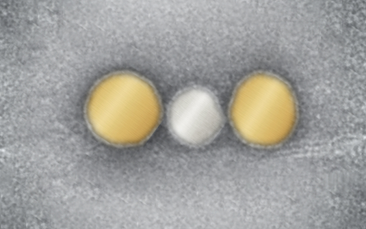
The research Group of Optical Detection and Sensing (GODS) have reported a three-terminal photonic synapse based on the large-area, uniform multilayer MoS2 films. The reported device realized ultrashort optical pulse detection within 5 μs and ultralow power consumption about 40 aJ, which means its performance is much better than the current reported properties of photonic synapses. Moreover, it is several orders of magnitude lower than the corresponding parameters of biological synapses, indicating that the reported photonic synapse can be further used for more complex ANN. The photoconductivity of MoS2 channel grown by CVD is regulated by photostimulation signal, which enables the device to simulate short-term synaptic plasticity (STP), long-term synaptic plasticity (LTP), paired-pulse facilitation (PPF) and other synaptic properties. Therefore, the reported photonic synapse can simulate human visual perception, and the detection wavelength can be extended to near infrared light. As the most important system of human learning, visual perception system can receive 80% of learning information from the outside. With the continuous development of AI, there is an urgent need for low-power and high sensitivity visual perception system that can effectively receive external information. In addition, with the assistant of gate voltage, this photonic synapse can simulate the classical Pavlovian conditioning and the regulation of different emotions on memory ability. For example, positive emotions enhance memory ability and negative emotions weaken memory ability. Furthermore, a significant contrast in the strength of STP and LTP based on the reported photonic synapse suggests that it can preprocess the input light signal. These results indicate that the photo-stimulation and backgate control can effectively regulate the conductivity of MoS2 channel layer by adjusting carrier trapping/detrapping processes. Moreover, the photonic synapse presented in this paper is expected to integrate sensing-memory-preprocessing capabilities, which can be used for real-time image detection and in-situ storage, and also provides the possibility to break the von Neumann bottleneck.
…
Here’s a link to and a citation for the paper,
Photonic synapses with ultralow energy consumption for artificial visual perception and brain storage by Caihong Li, Wen Du, Yixuan Huang, Jihua Zou, Lingzhi Luo, Song Sun, Alexander O. Govorov, Jiang Wu, Hongxing Xu, Zhiming Wang. Opto-Electron Adv Vol 5, No 9 210069 (2022). doi: 10.29026/oea.2022.210069
This paper is open access.
Observations
I don’t have much to say about the research itself other than, I believe this is the first time I’ve seen a news release about neuromorphic computing research from China.
it’s China that most interests me, especially these bits from the June 30, 2022 Compuscript Ltd news release on EurekAlert,
Group of Optical Detection and Sensing (GODS) [emphasis mine] was established in 2019. It is a research group focusing on compound semiconductors, lasers, photodetectors, and optical sensors. GODS has established a well-equipped laboratory with research facilities such as Molecular Beam Epitaxy system, IR detector test system, etc. GODS is leading several research projects funded by NSFC and National Key R&D Programmes. GODS have published more than 100 research articles in Nature Electronics, Light: Science and Applications, Advanced Materials and other international well-known high-level journals with the total citations beyond 8000.
Jiang Wu obtained his Ph.D. from the University of Arkansas Fayetteville in 2011. After his Ph.D., he joined UESTC as associate professor and later professor. He joined University College London [UCL] as a research associate in 2012 and then lecturer in the Department of Electronic and Electrical Engineering at UCL from 2015 to 2018. He is now a professor at UESTC [University of Electronic Science and Technology of China] [emphases mine]. His research interests include optoelectronic applications of semiconductor heterostructures. He is a Fellow of the Higher Education Academy and Senior Member of IEEE.
Opto-Electronic Advances (OEA) is a high-impact, open access, peer reviewed monthly SCI journal with an impact factor of 9.682 (Journals Citation Reports for IF 2020). Since its launch in March 2018, OEA has been indexed in SCI, EI, DOAJ, Scopus, CA and ICI databases over the time and expanded its Editorial Board to 36 members from 17 countries and regions (average h-index 49). [emphases mine]
The journal is published by The Institute of Optics and Electronics, Chinese Academy of Sciences, aiming at providing a platform for researchers, academicians, professionals, practitioners, and students to impart and share knowledge in the form of high quality empirical and theoretical research papers covering the topics of optics, photonics and optoelectronics.
The research group’s awkward name was almost certainly developed with the rather grandiose acronym, GODS, in mind. I don’t think you could get away with doing this in an English-speaking country as your colleagues would mock you mercilessly.
It’s Jiang Wu’s academic and work history that’s of most interest as it might provide insight into China’s Young Thousand Talents program. A January 5, 2023 American Association for the Advancement of Science (AAAS) news release describes the program,
In a systematic evaluation of China’s Young Thousand Talents (YTT) program, which was established in 2010, researchers find that China has been successful in recruiting and nurturing high-caliber Chinese scientists who received training abroad. Many of these individuals outperform overseas peers in publications and access to funding, the study shows, largely due to access to larger research teams and better research funding in China. Not only do the findings demonstrate the program’s relative success, but they also hold policy implications for the increasing number of governments pursuing means to tap expatriates for domestic knowledge production and talent development. China is a top sender of international students to United States and European Union science and engineering programs. The YTT program was created to recruit and nurture the productivity of high-caliber, early-career, expatriate scientists who return to China after receiving Ph.Ds. abroad. Although there has been a great deal of international attention on the YTT, some associated with the launch of the U.S.’s controversial China Initiative and federal investigations into academic researchers with ties to China, there has been little evidence-based research on the success, impact, and policy implications of the program itself. Dongbo Shi and colleagues evaluated the YTT program’s first 4 cohorts of scholars and compared their research productivity to that of their peers that remained overseas. Shi et al. found that China’s YTT program successfully attracted high-caliber – but not top-caliber – scientists. However, those young scientists that did return outperformed others in publications across journal-quality tiers – particularly in last-authored publications. The authors suggest that this is due to YTT scholars’ greater access to larger research teams and better research funding in China. The authors say the dearth of such resources in the U.S. and E.U. “may not only expedite expatriates’ return decisions but also motivate young U.S.- and E.U.-born scientists to seek international research opportunities.” They say their findings underscore the need for policy adjustments to allocate more support for young scientists.
Here’s a link to and a citation for the paper,
Has China’s Young Thousand Talents program been successful in recruiting and nurturing top-caliber scientists? by Dongbo Shi, Weichen Liu, and Yanbo Wang. Science 5 Jan 2023 Vol 379, Issue 6627 pp. 62-65 DOI: 10.1126/science.abq1218
This paper is behind a paywall.
Kudos to the folks behind China’s Young Thousands Talents program! Jiang Wu’s career appears to be a prime example of the program’s success. Perhaps Canadian policy makers will be inspired.