Tag Archives: Allister F. McGuire

A graphene ‘camera’ and your beating heart: say cheese

Comparing it to a ‘camera’, even with the quotes, is a bit of a stretch for my taste but I can’t come up with a better comparison. Here’s a video so you can judge for yourself,

Caption: This video repeats three times the graphene camera images of a single beat of an embryonic chicken heart. The images, separated by 5 milliseconds, were measured by a laser bouncing off a graphene sheet lying beneath the heart. The images are about 2 millimeters on a side. Credit: UC Berkeley images by Halleh Balch, Alister McGuire and Jason Horng

A June 16, 2021 news item on ScienceDaily announces the research,

Bay Area [San Francisco, California] scientists have captured the real-time electrical activity of a beating heart, using a sheet of graphene to record an optical image — almost like a video camera — of the faint electric fields generated by the rhythmic firing of the heart’s muscle cells.

A University of California at Berkeley (UC Berkeley) June 16, 2021 news release (also on EurekAlert) by Robert Sanders, which originated the news item, provides more detail,

The graphene camera represents a new type of sensor useful for studying cells and tissues that generate electrical voltages, including groups of neurons or cardiac muscle cells. To date, electrodes or chemical dyes have been used to measure electrical firing in these cells. But electrodes and dyes measure the voltage at one point only; a graphene sheet measures the voltage continuously over all the tissue it touches.

The development, published online last week in the journal Nano Letters, comes from a collaboration between two teams of quantum physicists at the University of California, Berkeley, and physical chemists at Stanford University.

“Because we are imaging all cells simultaneously onto a camera, we don’t have to scan, and we don’t have just a point measurement. We can image the entire network of cells at the same time,” said Halleh Balch, one of three first authors of the paper and a recent Ph.D. recipient in UC Berkeley’s Department of Physics.

While the graphene sensor works without having to label cells with dyes or tracers, it can easily be combined with standard microscopy to image fluorescently labeled nerve or muscle tissue while simultaneously recording the electrical signals the cells use to communicate.

“The ease with which you can image an entire region of a sample could be especially useful in the study of neural networks that have all sorts of cell types involved,” said another first author of the study, Allister McGuire, who recently received a Ph.D. from Stanford and. “If you have a fluorescently labeled cell system, you might only be targeting a certain type of neuron. Our system would allow you to capture electrical activity in all neurons and their support cells with very high integrity, which could really impact the way that people do these network level studies.”

Graphene is a one-atom thick sheet of carbon atoms arranged in a two-dimensional hexagonal pattern reminiscent of honeycomb. The 2D structure has captured the interest of physicists for several decades because of its unique electrical properties and robustness and its interesting optical and optoelectronic properties.

“This is maybe the first example where you can use an optical readout of 2D materials to measure biological electrical fields,” said senior author Feng Wang, UC Berkeley professor of physics. “People have used 2D materials to do some sensing with pure electrical readout before, but this is unique in that it works with microscopy so that you can do parallel detection.”

The team calls the tool a critically coupled waveguide-amplified graphene electric field sensor, or CAGE sensor.

“This study is just a preliminary one; we want to showcase to biologists that there is such a tool you can use, and you can do great imaging. It has fast time resolution and great electric field sensitivity,” said the third first author, Jason Horng, a UC Berkeley Ph.D. recipient who is now a postdoctoral fellow at the National Institute of Standards and Technology. “Right now, it is just a prototype, but in the future, I think we can improve the device.”

Graphene is sensitive to electric fields

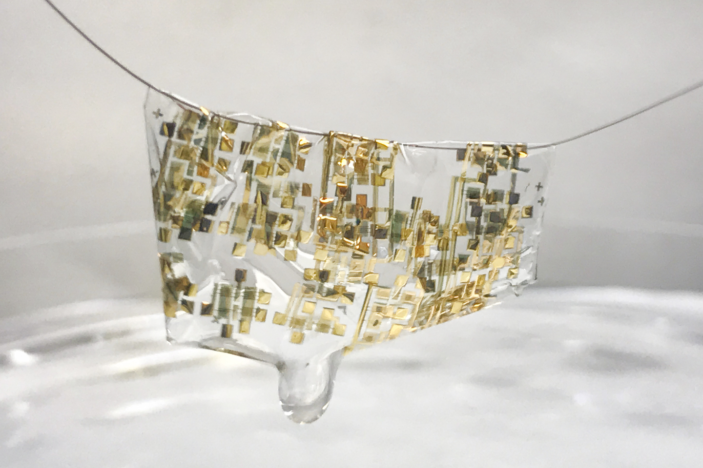
Ten years ago, Wang discovered that an electric field affects how graphene reflects or absorbs light. Balch and Horng exploited this discovery in designing the graphene camera. They obtained a sheet of graphene about 1 centimeter on a side produced by chemical vapor deposition in the lab of UC Berkeley physics professor Michael Crommie and placed on it a live heart from a chicken embryo, freshly extracted from a fertilized egg. These experiments were performed in the Stanford lab of Bianxiao Cui, who develops nanoscale tools to study electrical signaling in neurons and cardiac cells.

The team showed that when the graphene was tuned properly, the electrical signals that flowed along the surface of the heart during a beat were sufficient to change the reflectance of the graphene sheet.

“When cells contract, they fire action potentials that generate a small electric field outside of the cell,” Balch said. “The absorption of graphene right under that cell is modified, so we will see a change in the amount of light that comes back from that position on the large area of graphene.”

In initial studies, however, Horng found that the change in reflectance was too small to detect easily. An electric field reduces the reflectance of graphene by at most 2%; the effect was much less from changes in the electric field when the heart muscle cells fired an action potential.

Together, Balch, Horng and Wang found a way to amplify this signal by adding a thin waveguide below graphene, forcing the reflected laser light to bounce internally about 100 times before escaping. This made the change in reflectance detectable by a normal optical video camera.

“One way of thinking about it is that the more times that light bounces off of graphene as it propagates through this little cavity, the more effects that light feels from graphene’s response, and that allows us to obtain very, very high sensitivity to electric fields and voltages down to microvolts,” Balch said.

The increased amplification necessarily lowers the resolution of the image, but at 10 microns, it is more than enough to study cardiac cells that are several tens of microns across, she said.

Another application, McGuire said, is to test the effect of drug candidates on heart muscle before these drugs go into clinical trials to see whether, for example, they induce an unwanted arrhythmia. To demonstrate this, he and his colleagues observed the beating chicken heart with CAGE and an optical microscope while infusing it with a drug, blebbistatin, that inhibits the muscle protein myosin. They observed the heart stop beating, but CAGE showed that the electrical signals were unaffected.

Because graphene sheets are mechanically tough, they could also be placed directly on the surface of the brain to get a continuous measure of electrical activity — for example, to monitor neuron firing in the brains of those with epilepsy or to study fundamental brain activity. Today’s electrode arrays measure activity at a few hundred points, not continuously over the brain surface.

“One of the things that is amazing to me about this project is that electric fields mediate chemical interactions, mediate biophysical interactions — they mediate all sorts of processes in the natural world — but we never measure them. We measure current, and we measure voltage,” Balch said. “The ability to actually image electric fields gives you a look at a modality that you previously had little insight into.”

Here’s a link to and a citation for the paper,

Graphene Electric Field Sensor Enables Single Shot Label-Free Imaging of Bioelectric Potentials by Halleh B. Balch, Allister F. McGuire, Jason Horng, Hsin-Zon Tsai, Kevin K. Qi, Yi-Shiou Duh, Patrick R. Forrester, Michael F. Crommie, Bianxiao Cui, and Feng Wang. Nano Lett. 2021, XXXX, XXX, XXX-XXX OI: https://doi.org/10.1021/acs.nanolett.1c00543 Publication Date: June 8, 2021 © 2021 American Chemical Society

This paper is behind a paywall.

Gamechanging electronics with new ultrafast, flexible, and transparent electronics

There are two news bits about game-changing electronics, one from the UK and the other from the US.

United Kingdom (UK)

An April 3, 2017 news item on Azonano announces the possibility of a future golden age of electronics courtesy of the University of Exeter,

Engineering experts from the University of Exeter have come up with a breakthrough way to create the smallest, quickest, highest-capacity memories for transparent and flexible applications that could lead to a future golden age of electronics.

A March 31, 2017 University of Exeter press release (also on EurekAlert), which originated the news item, expands on the theme (Note: Links have been removed),

Engineering experts from the University of Exeter have developed innovative new memory using a hybrid of graphene oxide and titanium oxide. Their devices are low cost and eco-friendly to produce, are also perfectly suited for use in flexible electronic devices such as ‘bendable’ mobile phone, computer and television screens, and even ‘intelligent’ clothing.

Crucially, these devices may also have the potential to offer a cheaper and more adaptable alternative to ‘flash memory’, which is currently used in many common devices such as memory cards, graphics cards and USB computer drives.

The research team insist that these innovative new devices have the potential to revolutionise not only how data is stored, but also take flexible electronics to a new age in terms of speed, efficiency and power.

Professor David Wright, an Electronic Engineering expert from the University of Exeter and lead author of the paper said: “Using graphene oxide to produce memory devices has been reported before, but they were typically very large, slow, and aimed at the ‘cheap and cheerful’ end of the electronics goods market.

“Our hybrid graphene oxide-titanium oxide memory is, in contrast, just 50 nanometres long and 8 nanometres thick and can be written to and read from in less than five nanoseconds – with one nanometre being one billionth of a metre and one nanosecond a billionth of a second.”

Professor Craciun, a co-author of the work, added: “Being able to improve data storage is the backbone of tomorrow’s knowledge economy, as well as industry on a global scale. Our work offers the opportunity to completely transform graphene-oxide memory technology, and the potential and possibilities it offers.”

Here’s a link to and a citation for the paper,

Multilevel Ultrafast Flexible Nanoscale Nonvolatile Hybrid Graphene Oxide–Titanium Oxide Memories by V. Karthik Nagareddy, Matthew D. Barnes, Federico Zipoli, Khue T. Lai, Arseny M. Alexeev, Monica Felicia Craciun, and C. David Wright. ACS Nano, 2017, 11 (3), pp 3010–3021 DOI: 10.1021/acsnano.6b08668 Publication Date (Web): February 21, 2017

Copyright © 2017 American Chemical Society

This paper appears to be open access.

United States (US)

Researchers from Stanford University have developed flexible, biodegradable electronics.

A newly developed flexible, biodegradable semiconductor developed by Stanford engineers shown on a human hair. (Image credit: Bao lab)

A human hair? That’s amazing and this May 3, 2017 news item on Nanowerk reveals more,

As electronics become increasingly pervasive in our lives – from smart phones to wearable sensors – so too does the ever rising amount of electronic waste they create. A United Nations Environment Program report found that almost 50 million tons of electronic waste were thrown out in 2017–more than 20 percent higher than waste in 2015.

Troubled by this mounting waste, Stanford engineer Zhenan Bao and her team are rethinking electronics. “In my group, we have been trying to mimic the function of human skin to think about how to develop future electronic devices,” Bao said. She described how skin is stretchable, self-healable and also biodegradable – an attractive list of characteristics for electronics. “We have achieved the first two [flexible and self-healing], so the biodegradability was something we wanted to tackle.”

The team created a flexible electronic device that can easily degrade just by adding a weak acid like vinegar. The results were published in the Proceedings of the National Academy of Sciences (“Biocompatible and totally disintegrable semiconducting polymer for ultrathin and ultralightweight transient electronics”).

“This is the first example of a semiconductive polymer that can decompose,” said lead author Ting Lei, a postdoctoral fellow working with Bao.

A May 1, 2017 Stanford University news release by Sarah Derouin, which originated the news item, provides more detail,

In addition to the polymer – essentially a flexible, conductive plastic – the team developed a degradable electronic circuit and a new biodegradable substrate material for mounting the electrical components. This substrate supports the electrical components, flexing and molding to rough and smooth surfaces alike. When the electronic device is no longer needed, the whole thing can biodegrade into nontoxic components.

Biodegradable bits

Bao, a professor of chemical engineering and materials science and engineering, had previously created a stretchable electrode modeled on human skin. That material could bend and twist in a way that could allow it to interface with the skin or brain, but it couldn’t degrade. That limited its application for implantable devices and – important to Bao – contributed to waste.

Flexible, biodegradable semiconductor on an avacado

The flexible semiconductor can adhere to smooth or rough surfaces and biodegrade to nontoxic products. (Image credit: Bao lab)

Bao said that creating a robust material that is both a good electrical conductor and biodegradable was a challenge, considering traditional polymer chemistry. “We have been trying to think how we can achieve both great electronic property but also have the biodegradability,” Bao said.

Eventually, the team found that by tweaking the chemical structure of the flexible material it would break apart under mild stressors. “We came up with an idea of making these molecules using a special type of chemical linkage that can retain the ability for the electron to smoothly transport along the molecule,” Bao said. “But also this chemical bond is sensitive to weak acid – even weaker than pure vinegar.” The result was a material that could carry an electronic signal but break down without requiring extreme measures.

In addition to the biodegradable polymer, the team developed a new type of electrical component and a substrate material that attaches to the entire electronic component. Electronic components are usually made of gold. But for this device, the researchers crafted components from iron. Bao noted that iron is a very environmentally friendly product and is nontoxic to humans.

The researchers created the substrate, which carries the electronic circuit and the polymer, from cellulose. Cellulose is the same substance that makes up paper. But unlike paper, the team altered cellulose fibers so the “paper” is transparent and flexible, while still breaking down easily. The thin film substrate allows the electronics to be worn on the skin or even implanted inside the body.

From implants to plants

The combination of a biodegradable conductive polymer and substrate makes the electronic device useful in a plethora of settings – from wearable electronics to large-scale environmental surveys with sensor dusts.

“We envision these soft patches that are very thin and conformable to the skin that can measure blood pressure, glucose value, sweat content,” Bao said. A person could wear a specifically designed patch for a day or week, then download the data. According to Bao, this short-term use of disposable electronics seems a perfect fit for a degradable, flexible design.

And it’s not just for skin surveys: the biodegradable substrate, polymers and iron electrodes make the entire component compatible with insertion into the human body. The polymer breaks down to product concentrations much lower than the published acceptable levels found in drinking water. Although the polymer was found to be biocompatible, Bao said that more studies would need to be done before implants are a regular occurrence.

Biodegradable electronics have the potential to go far beyond collecting heart disease and glucose data. These components could be used in places where surveys cover large areas in remote locations. Lei described a research scenario where biodegradable electronics are dropped by airplane over a forest to survey the landscape. “It’s a very large area and very hard for people to spread the sensors,” he said. “Also, if you spread the sensors, it’s very hard to gather them back. You don’t want to contaminate the environment so we need something that can be decomposed.” Instead of plastic littering the forest floor, the sensors would biodegrade away.

As the number of electronics increase, biodegradability will become more important. Lei is excited by their advancements and wants to keep improving performance of biodegradable electronics. “We currently have computers and cell phones and we generate millions and billions of cell phones, and it’s hard to decompose,” he said. “We hope we can develop some materials that can be decomposed so there is less waste.”

Other authors on the study include Ming Guan, Jia Liu, Hung-Cheng Lin, Raphael Pfattner, Leo Shaw, Allister McGuire, and Jeffrey Tok of Stanford University; Tsung-Ching Huang of Hewlett Packard Enterprise; and Lei-Lai Shao and Kwang-Ting Cheng of University of California, Santa Barbara.

The research was funded by the Air Force Office for Scientific Research; BASF; Marie Curie Cofund; Beatriu de Pinós fellowship; and the Kodak Graduate Fellowship.

Here’s a link to and a citation for the team’s latest paper,

Biocompatible and totally disintegrable semiconducting polymer for ultrathin and ultralightweight transient electronics by Ting Lei, Ming Guan, Jia Liu, Hung-Cheng Lin, Raphael Pfattner, Leo Shaw, Allister F. McGuire, Tsung-Ching Huang, Leilai Shao, Kwang-Ting Cheng, Jeffrey B.-H. Tok, and Zhenan Bao. PNAS 2017 doi: 10.1073/pnas.1701478114 published ahead of print May 1, 2017

This paper is behind a paywall.

The mention of cellulose in the second item piqued my interest so I checked to see if they’d used nanocellulose. No, they did not. Microcrystalline cellulose powder was used to constitute a cellulose film but they found a way to render this film at the nanoscale. From the Stanford paper (Note: Links have been removed),

… Moreover, cellulose films have been previously used as biodegradable substrates in electronics (28⇓–30). However, these cellulose films are typically made with thicknesses well over 10 μm and thus cannot be used to fabricate ultrathin electronics with substrate thicknesses below 1–2 μm (7, 18, 19). To the best of our knowledge, there have been no reports on ultrathin (1–2 μm) biodegradable substrates for electronics. Thus, to realize them, we subsequently developed a method described herein to obtain ultrathin (800 nm) cellulose films (Fig. 1B and SI Appendix, Fig. S8). First, microcrystalline cellulose powders were dissolved in LiCl/N,N-dimethylacetamide (DMAc) and reacted with hexamethyldisilazane (HMDS) (31, 32), providing trimethylsilyl-functionalized cellulose (TMSC) (Fig. 1B). To fabricate films or devices, TMSC in chlorobenzene (CB) (70 mg/mL) was spin-coated on a thin dextran sacrificial layer. The TMSC film was measured to be 1.2 μm. After hydrolyzing the film in 95% acetic acid vapor for 2 h, the trimethylsilyl groups were removed, giving a 400-nm-thick cellulose film. The film thickness significantly decreased to one-third of the original film thickness, largely due to the removal of the bulky trimethylsilyl groups. The hydrolyzed cellulose film is insoluble in most organic solvents, for example, toluene, THF, chloroform, CB, and water. Thus, we can sequentially repeat the above steps to obtain an 800-nm-thick film, which is robust enough for further device fabrication and peel-off. By soaking the device in water, the dextran layer is dissolved, starting from the edges of the device to the center. This process ultimately releases the ultrathin substrate and leaves it floating on water surface (Fig. 3A, Inset).

Finally, I don’t have any grand thoughts; it’s just interesting to see different approaches to flexible electronics.