Tag Archives: Andrea Alù

A couple of proposed solutions to AI’s insatiable need for power?

I have two stories about research into making artificial intelligence (AI) less wasteful of power. One is from the International Society for Optics and Photonics (SPIE) and the other from the Politecnico di Milano (Polytechnic of Milan).

International Society for Optics and Photonics (SPIE)

A September 9, 2025 news item on ScienceDaily announced a more energy efficient AI chip,

Artificial intelligence (AI) systems are increasingly central to technology, powering everything from facial recognition to language translation. But as AI models grow more complex, they consume vast amounts of electricity — posing challenges for energy efficiency and sustainability. A new chip developed by researchers at the University of Florida could help address this issue by using light, rather than just electricity, to perform one of AI’s most power-hungry tasks. Their research is reported in Advanced Photonics.

A September 8, 2025 SPIE (International Society for Optics and Photonics) press release, which originated the news item, provides more detail about the work, Note: Links have been removed,

The chip is designed to carry out convolution operations, a core function in machine learning that enables AI systems to detect patterns in images, video, and text. These operations typically require significant computing power. By integrating optical components directly onto a silicon chip, the researchers have created a system that performs convolutions using laser light and microscopic lenses—dramatically reducing energy consumption and speeding up processing.

“Performing a key machine learning computation at near zero energy is a leap forward for future AI systems,” said study leader Volker J. Sorger, the Rhines Endowed Professor in Semiconductor Photonics at the University of Florida. “This is critical to keep scaling up AI capabilities in years to come.”

In tests, the prototype chip classified handwritten digits with about 98 percent accuracy, comparable to traditional electronic chips. The system uses two sets of miniature Fresnel lenses—flat, ultrathin versions of the lenses found in lighthouses—fabricated using standard semiconductor manufacturing techniques. These lenses are narrower than a human hair and are etched directly onto the chip.

To perform a convolution, machine learning data is first converted into laser light on the chip. The light passes through the Fresnel lenses, which carry out the mathematical transformation. The result is then converted back into a digital signal to complete the AI task.

“This is the first time anyone has put this type of optical computation on a chip and applied it to an AI neural network,” said Hangbo Yang, a research associate professor in Sorger’s group at UF and co-author of the study.

The team also demonstrated that the chip could process multiple data streams simultaneously by using lasers of different colors—a technique known as wavelength multiplexing. “We can have multiple wavelengths, or colors, of light passing through the lens at the same time,” Yang said. “That’s a key advantage of photonics.”

The research was conducted in collaboration with the Florida Semiconductor Institute, UCLA [University of California at Los Angeles], and George Washington University. Sorger noted that chip manufacturers such as NVIDIA already use optical elements in some parts of their AI systems, which could make it easier to integrate this new technology.

“In the near future, chip-based optics will become a key part of every AI chip we use daily,” Sorger said. “And optical AI computing is next.”

There’s also a September 8, 2025 University of Florida news release (also on EurekAlert), which is similar to the one issued by SPIE.

The paper has been published on two different sites; the citation for the paper remains the same and there are links to two different sites hosting the paper,

Near-energy-free photonic Fourier transformation for convolution operation acceleration by Hangbo Yang, Nicola Peserico, Shurui Li, Xiaoxuan Ma, Russell L. T. Schwartz, Mostafa Hosseini, Aydin Babakhani, Chee Wei Wong, Puneet Gupta, Volker J. Sorger SPIE Digital library or Advanced Photonics Vol. 7, Issue 5, 056007 (2025) DOI: 10.1117/1.AP.7.5.056007

Both sites offer open access to the paper.

Politecnico di Milano (Polytechnic of Milan)

Caption: The photonic microchip (below) developed for the study on physical neural networks, along with the electronic chip (above, the yellow one) of control. Credit: Politecnico di Milano, DEIB – Department of Electronics, Information and Bioengineering

A September 12, 2025 Politecnico di Milano (Polytechnic of Milan) press release (also on EurekAlert but published September 9, 2025) announces work into a more energy efficient way to train artificial intelligence, specifically physical neural networks,

Artificial intelligence is now part of our daily lives, with the subsequent pressing need for larger, more complex models. However, the demand for ever-increasing power and computing capacity is rising faster than the performance traditional computers can provide.

To overcome these limitations, research is moving towards innovative technologies such as physical neural networks, analogue circuits that directly exploit the laws of physics (properties of light beams, quantum phenomena) to process information. Their potential is at the heart of the study published by the prestigious journal Nature. It is the outcome of collaboration between several international institutes, including the Politecnico di Milano, the École Polytechnique Fédérale in Lausanne, Stanford University, the University of Cambridge, and the Max Planck Institute.

The article entitled “Training of Physical Neural Networks” discusses the steps of research on training physical neural networks, carried out with the collaboration of Francesco Morichetti, professor at DEIB – Department of Electronics, Information and Bioengineering, and head of the university’s Photonic Devices Lab.

Politecnico di Milano contributed to this study by developing photonic chips for the creation of neural networks, exploiting integrated photonic technologies. Mathematical operations, such as sums and multiplications, can now be performed through light interference mechanisms on silicon microchips barely a few square millimetres in size.

By eliminating the operations required for the digitisation of information, our photonic chips allow calculations to be carried out with a significant reduction in both energy consumption and processing time,” says Francesco Morichetti. A step forward to make artificial intelligence (which relies on extremely energy-intensive data centres) more sustainable.

The study published in Nature addresses the theme of training, precisely the phase in which the network learns to perform certain tasks. «With our research within the Department of Electronics, Information and Bioengineering, we have helped develop an “in-situ” training technique for photonic neural networks, i.e. without going through digital models. The procedure is carried out entirely using light signals. Hence, network training will not only be faster, but also more robust and efficient», adds Morichetti.

The use of photonic chips will allow the development of more sophisticated models for artificial intelligence, or devices capable of processing real-time data directly on site – such as autonomous cars or intelligent sensors integrated into portable devices – without requiring remote processing.

Here’s a link to and a citation for the paper,

Training of physical neural networks by Ali Momeni, Babak Rahmani, Benjamin Scellier, Logan G. Wright, Peter L. McMahon, Clara C. Wanjura, Yuhang Li, Anas Skalli, Natalia G. Berloff, Tatsuhiro Onodera, Ilker Oguz, Francesco Morichetti, Philipp del Hougne, Manuel Le Gallo, Abu Sebastian, Azalia Mirhoseini, Cheng Zhang, Danijela Marković, Daniel Brunner, Christophe Moser, Sylvain Gigan, Florian Marquardt, Aydogan Ozcan, Julie Grollier, Andrea J. Liu, Demetri Psaltis, Andrea Alù, Romain Fleury. Nature volume 645, pages 53–61 (2025) DOI: https://doi.org/10.1038/s41586-025-09384-2 Published: 03 September 2025 Version of record: 03 September 2025 Issue date: 04 September 2025

This paper is behind a paywall.

Tunable metasurfaces and reshaping the future of light

Thinner, meaning smaller and less bulky, is a prized quality in technologies such as phones, batteries, and, in this case, lenses. From a May 16, 2022 news item on ScienceDaily,

The technological advancement of optical lenses has long been a significant marker of human scientific achievement. Eyeglasses, telescopes, cameras, and microscopes have all literally and figuratively allowed us to see the world in a new light. Lenses are also a fundamental component of manufacturing nanoelectronics by the semiconductor industry.

One of the most impactful breakthroughs of lens technology in recent history has been the development of photonic metasurfaces — artificially engineered nano-scale materials with remarkable optical properties. Georgia Tech [Georgia Institute of Technology] researchers at the forefront of this technology have recently demonstrated the first-ever electrically tunable photonic metasurface platform in a recent study published by Nature Communications.

“Metasurfaces can make the optical systems very thin, and as they become easier to control and tune, you’ll soon find them in cell phone cameras and similar electronic imaging systems,” said Ali Adibi, professor in the School of Electrical and Computer Engineering at the Georgia Institute of Technology [Georgia Tech; US].

A May 10, 2022 Georgia Tech news release (also on EurekAlert but published May 16, 2022), which originated the news item, provides more detail,

The pronounced tuning measures achieved through the new platform represent a critical advancement towards the development of miniaturized reconfigurable metasurfaces. The results of the study have shown a record eleven-fold change in the reflective properties, a large range of spectral tuning for operation, and much faster tuning speed.

Heating Up Metasurfaces

Metasurfaces are a class of nanophotonic materials in which a large range of miniaturized elements are engineered to affect the transmission and reflection of light at different frequencies in a controlled way.

“When viewing under very strong microscopes, metasurfaces look like a periodic array of posts,” said Adibi. “The best analogy would be to think of a LEGO pattern formed by connecting many similar LEGO bricks next to each other.”

Since their inception, metasurfaces have been used to demonstrate that very thin optical devices can affect light propagation with metalenses (the formation of thin lenses) being the most developed application.

Despite impressive progress, most demonstrated metasurfaces are passive, meaning their performance cannot be changed (or tuned) after fabrication. The work presented by Adibi and his team, led by Ph.D. candidate Sajjad Abdollahramezani, applies electrical heat to a special class of nanophotonic materials to create a platform that can enable reconfigurable metasurfaces to be easily manufactured with high levels of optical modulation.

PCMs Provide the Answer

A wide range of materials may be used to form metasurfaces including metals, oxides, and semiconductors, but Abdollahramezani and Adibi’s research focuses on phase-change materials (PCMs) because they can form the most effective structures with the smallest feature sizes. PCMs are substances that absorb and release heat during the process of heating and cooling. They are called “phase-change” materials because they go from one crystallization state to another during the thermal cycling process. Water changing from a liquid to a solid or gas is the most common example.

The Georgia Tech team’s experiments are substantially more complicated than heating and freezing water. Knowing that the optical properties of PCMs can be altered by local heating, they have harnessed the full potential of the PCM alloy Ge2Sb2Te5 (GST), which is a compound of germanium, antimony, and tellurium.

By combining the optical design with a miniaturized electrical microheater underneath, the team can change the crystalline phase of the GST to make active tuning of the metasurface device possible. The fabricated metasurfaces were developed at Georgia Tech’s Institute for Electronics and Nanotechnology (IEN) and tested in characterization labs by illuminating the reconfigurable metasurfaces with laser light at different frequencies and measuring the properties of the reflected light in real time.

What Tunable Metasurfaces Mean for the Future

Driven by device miniaturization and system integration, as well as their ability to selectively reflect different colors of light, metasurfaces are rapidly replacing bulky optical assemblies of the past. Immediate impact on technologies like LiDAR systems for autonomous cars, imaging, spectroscopy, and sensing is expected.

With further development, more aggressive applications like computing, augmented reality, photonic chips for artificial intelligence, and biohazard detection can also be envisioned, according to Abdollahramezani and Adibi.

“As the platform continues to develop, reconfigurable metasurfaces will be found everywhere,” said Adibi. “They will even empower smaller endoscopes to go deep inside the body for better imaging and help medical sensors detect different biomarkers in blood.”

Funding: This material is based upon work supported by the National Science Foundation (NSF) under Grant No. 1837021. Any opinions, findings, and conclusions or recommendations expressed in this material are those of the authors and do not necessarily reflect the views of the NSF. The work was primarily funded by Office of Naval Research (ONR) (N00014-18-1-2055, Dr. B. Bennett) and by Defense Advanced Research Projects Agency [DARPA] (D19AC00001, Dr. R. Chandrasekar). W.C. acknowledges support from ONR (N00014-17-1-2555) and National Science Foundation (NSF) (DMR-2004749). A. Alù acknowledges support from Air Force Office of Scientific Research and the Simons Foundation. M.W. acknowledges support by the Deutsche Forschungsgemeinschaft (SFB 917). M.E.S. acknowledges financial support of NSF-CHE (1608801). This work was performed in part at the Georgia Tech Institute for Electronics and Nanotechnology (IEN), a member of the National Nanotechnology Coordinated Infrastructure (NNCI), which is supported by NSF (ECCS1542174).

Caption: Georgia Tech professor Ali Adibi [on the right] with Ph.D. candidate Sajjad Abdollahramezani [on th eleft holding an unidentified object] in Ali’s Photonics Research Group lab where the characterization of the tunable metasurfaces takes place. Credit: Georgia Tech

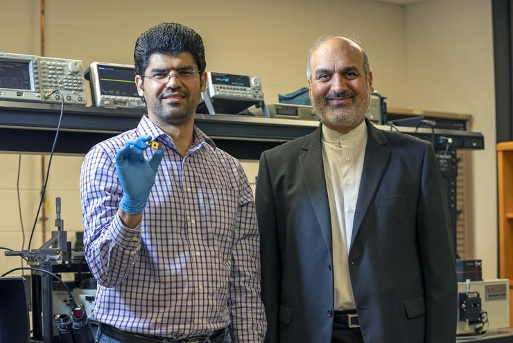
I am charmed by this image. Neither of these two are professionals at posing for photographers. Nonetheless, they look pleased and happy to help the publicity team spread the word about their research, they also seem like they’re looking forward to getting back to work.

Here’s a link to and a citation for the paper,

Electrically driven reprogrammable phase-change metasurface reaching 80% efficiency by Sajjad Abdollahramezani, Omid Hemmatyar, Mohammad Taghinejad, Hossein Taghinejad, Alex Krasnok, Ali A. Eftekhar, Christian Teichrib, Sanchit Deshmukh, Mostafa A. El-Sayed, Eric Pop, Matthias Wuttig, Andrea Alù, Wenshan Cai & Ali Adibi. Nature Communications volume 13, Article number: 1696 (2022) DOI: https://doi.org/10.1038/s41467-022-29374-6 Published: 30 March 2022

This paper is open access.

Exploring the fundamental limits of invisibility cloaks

There’s some interesting work on invisibility cloaks coming from the University of Texas at Austin according to a July 6, 2015 news item on Nanowerk,

Researchers in the Cockrell School of Engineering at The University of Texas at Austin have been able to quantify fundamental physical limitations on the performance of cloaking devices, a technology that allows objects to become invisible or undetectable to electromagnetic waves including radio waves, microwaves, infrared and visible light.

A July 5, 2016 University of Texas at Austin news release (also on EurekAlert), which originated the news item, expands on the theme,

The researchers’ theory confirms that it is possible to use cloaks to perfectly hide an object for a specific wavelength, but hiding an object from an illumination containing different wavelengths becomes more challenging as the size of the object increases.

Andrea Alù, an electrical and computer engineering professor and a leading researcher in the area of cloaking technology, along with graduate student Francesco Monticone, created a quantitative framework that now establishes boundaries on the bandwidth capabilities of electromagnetic cloaks for objects of different sizes and composition. As a result, researchers can calculate the expected optimal performance of invisibility devices before designing and developing a specific cloak for an object of interest. …

Cloaks are made from artificial materials, called metamaterials, that have special properties enabling a better control of the incoming wave, and can make an object invisible or transparent. The newly established boundaries apply to cloaks made of passive metamaterials — those that do not draw energy from an external power source.

Understanding the bandwidth and size limitations of cloaking is important to assess the potential of cloaking devices for real-world applications such as communication antennas, biomedical devices and military radars, Alù said. The researchers’ framework shows that the performance of a passive cloak is largely determined by the size of the object to be hidden compared with the wavelength of the incoming wave, and it quantifies how, for shorter wavelengths, cloaking gets drastically more difficult.

For example, it is possible to cloak a medium-size antenna from radio waves over relatively broad bandwidths for clearer communications, but it is essentially impossible to cloak large objects, such as a human body or a military tank, from visible light waves, which are much shorter than radio waves.

“We have shown that it will not be possible to drastically suppress the light scattering of a tank or an airplane for visible frequencies with currently available techniques based on passive materials,” Monticone said. “But for objects comparable in size to the wavelength that excites them (a typical radio-wave antenna, for example, or the tip of some optical microscopy tools), the derived bounds show that you can do something useful, the restrictions become looser, and we can quantify them.”

In addition to providing a practical guide for research on cloaking devices, the researchers believe that the proposed framework can help dispel some of the myths that have been developed around cloaking and its potential to make large objects invisible.
“The question is, ‘Can we make a passive cloak that makes human-scale objects invisible?’ ” Alù said. “It turns out that there are stringent constraints in coating an object with a passive material and making it look as if the object were not there, for an arbitrary incoming wave and observation point.”

Now that bandwidth limits on cloaking are available, researchers can focus on developing practical applications with this technology that get close to these limits.

“If we want to go beyond the performance of passive cloaks, there are other options,” Monticone said. “Our group and others have been exploring active and nonlinear cloaking techniques, for which these limits do not apply. Alternatively, we can aim for looser forms of invisibility, as in cloaking devices that introduce phase delays as light is transmitted through, camouflaging techniques, or other optical tricks that give the impression of transparency, without actually reducing the overall scattering of light.”

Alù’s lab is working on the design of active cloaks that use metamaterials plugged to an external energy source to achieve broader transparency bandwidths.

“Even with active cloaks, Einstein’s theory of relativity fundamentally limits the ultimate performance for invisibility,” Alù said. “Yet, with new concepts and designs, such as active and nonlinear metamaterials, it is possible to move forward in the quest for transparency and invisibility.”

The researchers have prepared a diagram illustrating their work,

The graph shows the trade-off between how much an object can be made transparent (scattering reduction; vertical axis) and the color span (bandwidth; horizontal axis) over which this phenomenon can be achieved. Courtesy: University of Texas at Austin

The graph shows the trade-off between how much an object can be made transparent (scattering reduction; vertical axis) and the color span (bandwidth; horizontal axis) over which this phenomenon can be achieved. Courtesy: University of Texas at Austin

Here’s a link to and a citation for the paper,

Invisibility exposed: physical bounds on passive cloaking by Francesco Monticone and Andrea Alù. Optica Vol. 3, Issue 7, pp. 718-724 (2016) •doi: 10.1364/OPTICA.3.000718

This paper is open access.

Battery-powered invisibiity cloak

You’d never guess it from the title of their paper but researchers at the University of Texas at Austin have conceptualized and designed a battery-operated invisibility cloak, according to a Dec. 18, 2013 news item on Nanowerk,

Researchers at The University of Texas at Austin have proposed the first design of a cloaking device that uses an external source of energy to significantly broaden its bandwidth of operation.

Andrea Alù, associate professor in the Department of Electrical and Computer Engineering at the Cockrell School of Engineering, and his team have proposed a design for an active cloak that draws energy from a battery, allowing objects to become undetectable to radio sensors over a greater range of frequencies.

The Dec. 18, 2013 University of Texas at Austin news release (also on EurekAlert), which originated the news item, describes the current state of cloaking technology,

Cloaks have so far been realized with so-called passive technology, which means that they are not designed to draw energy from an external source. They are typically based on metamaterials (advanced artificial materials) or metasurfaces (a flexible, ultrathin metamaterial) that can suppress the scattering of light that bounces off an object, making an object less visible. When the scattered fields from the cloak and the object interfere, they cancel each other out, and the overall effect is transparency to radio-wave detectors. They can suppress 100 times or more the detectability at specific design frequencies. Although the proposed design works for radio waves, active cloaks could one day be designed to make detection by the human eye more difficult.

“Many cloaking designs are good at suppressing the visibility under certain conditions, but they are inherently limited to work for specific colors of light or specific frequencies of operation,” said Alù, David & Doris Lybarger Endowed Faculty Fellow in the Department of Electrical and Computer Engineering. In this paper, on the contrary, “we prove that cloaks can become broadband, pushing this technology far beyond current limits of passive cloaks. I believe that our design helps us understand the fundamental challenges of suppressing the scattering of various objects at multiple wavelengths and shows a realistic path to overcome them.”

The news release details the new battery-powered design,

The proposed active cloak uses a battery, circuits and amplifiers to boost signals, which makes possible the reduction of scattering over a greater range of frequencies. This design, which covers a very broad frequency range, will provide the most broadband and robust performance of a cloak to date. Additionally, the proposed active technology can be thinner and less conspicuous than conventional cloaks.

In a related paper, published in Physical Review X in October, Alù and his graduate student Francesco Monticone proved that existing passive cloaking solutions are fundamentally limited in the bandwidth of operation and cannot provide broadband cloaking. When viewed at certain frequencies, passively cloaked objects may indeed become transparent, but if illuminated with white light, which is composed of many colors, they are bound to become more visible with the cloak than without. The October paper proves that all available cloaking techniques based on passive cloaks are constrained by Foster’s theorem, which limits their overall ability to cancel the scattering across a broad frequency spectrum.

In contrast, an active cloak based on active metasurfaces, such as the one designed by Alù’s team, can break Foster’s theorem limitations. The team started with a passive metasurface made from an array of metal square patches and loaded it with properly positioned operational amplifiers that use the energy drawn from a battery to broaden the bandwidth.

“In our case, by introducing these suitable amplifiers along the cloaking surface, we can break the fundamental limits of passive cloaks and realize a ‘non-Foster’ surface reactance that decreases, rather than increases, with frequency, significantly broadening the bandwidth of operation,” Alù said.

The researchers are continuing to work both on the theory and design behind their non-Foster active cloak, and they plan to build a prototype.

Alù and his team are working to use active cloaks to improve wireless communications by suppressing the disturbance that neighboring antennas produce on transmitting and receiving antennas. They have also proposed to use these cloaks to improve biomedical sensing, near-field imaging and energy harvesting devices.

Here’s a link to and a citation for the team’s paper about active cloaking,

Broadening the Cloaking Bandwidth with Non-Foster Metasurfaces by Pai-Yen Chen, Christos Argyropoulos, and Andrea Alù. Phys. Rev. Lett. 111, 233001 (2013) [5 pages] DOI: 10.1103/PhysRevLett.111.233001

This paper is behind a paywall.

Here’s a link to and a citation for the related and previously published paper (authors: Alù and Monticone),

Do Cloaked Objects Really Scatter Less? by Francesco Monticone and Andrea Alù. Phys. Rev. X 3, 041005 (2013) [10 pages] DOI: 10.1103/PhysRevX.3.041005

The authors have included both an abstract and a popular summary. I’ve excerpted the popular summary,

From ancient times, humanity has been fascinated by the concept of invisibility, and recently, scientists have moved a step closer to bringing this idea to reality by exploiting engineered artificial materials, or metamaterials. Several recent studies have indeed shown that a properly tailored metamaterial cover can, in principle, render an object invisible when illuminated by an electromagnetic wave oscillating at the specific frequency of interest. Yet, experimental realizations and theoretical investigations have consistently shown that reducing the visibility of an object with a passive cloak in a specific window of the electromagnetic spectrum is generally accompanied by a drastic increase of its visibility in other frequency ranges. Making an object invisible to red light, for instance, may actually make it bright blue, increasing its overall visibility.

In this paper, we quantitatively assess the potentials and limitations of passive cloaks in terms of overall visibility, integrated over the entire frequency spectrum. Quite surprisingly, our results show that any linear, causal, and passive invisibility cloak, without special superconducting features, is deemed to increase the scattering and visibility of the original uncloaked object, when integrated over all frequencies. This result confirms that the most popular cloaking devices actually scatter more, not less, when considered over a sufficiently broad frequency range, allowing easy detection using, e.g., pulsed excitation.

Our general theorem holds a relevant exception if specific covers with a strong static diamagnetism are considered, and, based on this principle, we propose a technique to reduce the global scattering, as well as the local response around a frequency of interest, using diamagnetic and superconducting thin cloaking layers. More generally, our results provide a quantitative measure to compare the overall performance of different cloaking devices and generally assess their detectability. These findings may open important research directions in the quest for invisibility, not only in the electromagnetic domain but also for acoustic, mechanical, and matter waves.

This is an open access paper.