Tag Archives: Andrea C. Ferrari

Human lung enzyme can degrade graphene

Caption: A human lung enzyme can biodegrade graphene. Credit: Fotolia Courtesy: Graphene Flagship

The big European Commission research programme, Grahene Flagship, has announced some new work with widespread implications if graphene is to be used in biomedical implants. From a August 23, 2018 news item on ScienceDaily,

Myeloperoxidase — an enzyme naturally found in our lungs — can biodegrade pristine graphene, according to the latest discovery of Graphene Flagship partners in CNRS, University of Strasbourg (France), Karolinska Institute (Sweden) and University of Castilla-La Mancha (Spain). Among other projects, the Graphene Flagship designs based like flexible biomedical electronic devices that will interfaced with the human body. Such applications require graphene to be biodegradable, so our body can be expelled from the body.

An August 23, 2018 Grapehene Flagship press release (mildly edited version on EurekAlert), which originated the news item, provides more detail,

To test how graphene behaves within the body, researchers analysed how it was broken down with the addition of a common human enzyme – myeloperoxidase or MPO. If a foreign body or bacteria is detected, neutrophils surround it and secrete MPO, thereby destroying the threat. Previous work by Graphene Flagship partners found that MPO could successfully biodegrade graphene oxide.

However, the structure of non-functionalized graphene was thought to be more resistant to degradation. To test this, the team looked at the effects of MPO ex vivo on two graphene forms; single- and few-layer.

Alberto Bianco, researcher at Graphene Flagship Partner CNRS, explains: “We used two forms of graphene, single- and few-layer, prepared by two different methods in water. They were then taken and put in contact with myeloperoxidase in the presence of hydrogen peroxide. This peroxidase was able to degrade and oxidise them. This was really unexpected, because we thought that non-functionalized graphene was more resistant than graphene oxide.”

Rajendra Kurapati, first author on the study and researcher at Graphene Flagship Partner CNRS, remarks how “the results emphasize that highly dispersible graphene could be degraded in the body by the action of neutrophils. This would open the new avenue for developing graphene-based materials.”

With successful ex-vivo testing, in-vivo testing is the next stage. Bengt Fadeel, professor at Graphene Flagship Partner Karolinska Institute believes that “understanding whether graphene is biodegradable or not is important for biomedical and other applications of this material. The fact that cells of the immune system are capable of handling graphene is very promising.”

Prof. Maurizio Prato, the Graphene Flagship leader for its Health and Environment Work Package said that “the enzymatic degradation of graphene is a very important topic, because in principle, graphene dispersed in the atmosphere could produce some harm. Instead, if there are microorganisms able to degrade graphene and related materials, the persistence of these materials in our environment will be strongly decreased. These types of studies are needed.” “What is also needed is to investigate the nature of degradation products,” adds Prato. “Once graphene is digested by enzymes, it could produce harmful derivatives. We need to know the structure of these derivatives and study their impact on health and environment,” he concludes.

Prof. Andrea C. Ferrari, Science and Technology Officer of the Graphene Flagship, and chair of its management panel added: “The report of a successful avenue for graphene biodegradation is a very important step forward to ensure the safe use of this material in applications. The Graphene Flagship has put the investigation of the health and environment effects of graphene at the centre of its programme since the start. These results strengthen our innovation and technology roadmap.”

Here’s a link to and a citation for the paper,

Degradation of Single‐Layer and Few‐Layer Graphene by Neutrophil Myeloperoxidase by Dr. Rajendra Kurapati, Dr. Sourav P. Mukherjee, Dr. Cristina Martín, Dr. George Bepete, Prof. Ester Vázquez, Dr. Alain Pénicaud, Prof. Dr. Bengt Fadeel, Dr. Alberto Bianco. Angewandte Chemie https://doi.org/10.1002/anie.201806906 First published: 13 July 2018

This paper is behind a paywall.

Making spider silk stronger by feeding graphene and carbon nanotubes to spiders

Spider silk is already considered a strong and tough material but now scientists have found a way to enhance those properties. From an August 15, 2017 Institute of Physics Publishing press release (also on EurekAlert),

…  researchers in Italy and the UK have found a way to make Spidey’s silk a lot stronger, using various different spider species and carbon nanotubes or graphene.

The research team, led by Professor Nicola Pugno at the University of Trento, Italy, succeeded in having their spiders produce silk with up to three times the strength and ten times the toughness of the regular material.

Their discovery, published today in the journal 2D Materials, could pave the way for a new class of bionicomposites, with a wide variety of uses.

Professor Pugno said: “Humans have used silkworm silks widely for thousands of years, but recently research has focussed on spider silk, as it has extremely promising mechanical properties. It is among the best spun polymer fibres in terms of tensile strength, ultimate strain, and especially toughness, even when compared to synthetic fibres such as Kevlar.

“We already know that there are biominerals present in in the protein matrices and hard tissues of insects, which gives them high strength and hardness in their jaws, mandibles and teeth, for example. So our study looked at whether spider silk’s properties could be ‘enhanced’ by artificially incorporating various different nanomaterials into the silk’s biological protein structures.”

To do this, the team exposed three different spider species to water dispersions containing carbon nanotubes or graphene.

After collecting the spiders’ silk, the team tested its tensile strength and toughness.

Professor Pugno said: “We found that the strongest silk the spiders spun had a fracture strength up to 5.4 gigapascals (GPa), and a toughness modulus up to 1,570 joules per gram (J/g). Normal spider silk, by comparison, has a fracture strength of around 1.5 GPa and a toughness modulus of around 150 J/g.

“This is the highest fibre toughness discovered to date, and a strength comparable to that of the strongest carbon fibres or limpet teeth. These are still early days, but our results are a proof of concept that paves the way to exploiting the naturally efficient spider spinning process to produce reinforced bionic silk fibres, thus further improving one of the most promising strong materials.

“These silks’ high toughness and resistance to ultimate strain could have applications such as parachutes.”

“Furthermore, this process of the natural integration of reinforcements in biological structural materials could also be applied to other animals and plants, leading to a new class of “bionicomposites” for innovative applications.”

Remember this? “You are what you eat.” If you’ve ever had doubts about that saying, these spiders should be laying them to rest.

Sadly, this news release doesn’t explain much about the decision to feed the spiders graphene or carbon nanotubes, which are identical other than in their respective shapes (sheet vs tube)  and whether those shapes did or did not affect the strength of the silk.

Here’s a link to and a citation for the paper,

Spider silk reinforced by graphene or carbon nanotubes by Emiliano Lepore, Federico Bosia, Francesco Bonaccorso, Matteo Bruna, Simone Taioli, Giovanni Garberoglio, Andrea C Ferrari, and Nicola Maria Pugno. 2D Materials, Volume 4, Number 3 DOI: https://doi.org/10.1088/2053-1583/aa7cd3 Published 14 August 2017

© 2017 IOP Publishing Ltd

This paper is behind a paywall.

Pugno was most recently mentioned here in a May 29, 2015 posting where he was listed as an author for a paper on synthesizing spider silk. Prior to 2015 I was familiar with Pugno’s name due to his work on adhesiveness in geckos.

Graphene Flagship high points

The European Union’s Graphene Flagship project has provided a series of highlights in place of an overview for the project’s ramp-up phase (in 2013 the Graphene Flagship was announced as one of two winners of a science competition, the other winner was the Human Brain Project, with two prizes of 1B Euros for each project). Here are the highlights from the April 19, 2016 Graphene Flagship press release,

Graphene and Neurons – the Best of Friends

Flagship researchers have shown that it is possible to interface untreated graphene with neuron cells whilst maintaining the integrity of these vital cells [1]. This result is a significant first step towards using graphene to produce better deep brain implants which can both harness and control the brain.

Graphene and Neurons
 

This paper emerged from the Graphene Flagship Work Package Health and Environment. Prof. Prato, the WP leader from the University of Trieste in Italy, commented that “We are currently involved in frontline research in graphene technology towards biomedical applications, exploring the interactions between graphene nano- and micro-sheets with the sophisticated signalling machinery of nerve cells. Our work is a first step in that direction.”

[1] Fabbro A., et al., Graphene-Based Interfaces do not Alter Target Nerve Cells. ACS Nano, 10 (1), 615 (2016).

Pressure Sensing with Graphene: Quite a Squeeze

The Graphene Flagship developed a small, robust, highly efficient squeeze film pressure sensor [2]. Pressure sensors are present in most mobile handsets and by replacing current sensor membranes with a graphene membrane they allow the sensor to decrease in size and significantly increase its responsiveness and lifetime.

Discussing this work which emerged from the Graphene Flagship Work Package Sensors is the paper’s lead author, Robin Dolleman from the Technical University of Delft in The Netherlands “After spending a year modelling various systems the idea of the squeeze-film pressure sensor was formed. Funding from the Graphene Flagship provided the opportunity to perform the experiments and we obtained very good results. We built a squeeze-film pressure sensor from 31 layers of graphene, which showed a 45 times higher response than silicon based devices, while reducing the area of the device by a factor of 25. Currently, our work is focused on obtaining similar results on monolayer graphene.”


[2] Dolleman R. J. et al., Graphene Squeeze-Film Pressure Sensors. Nano Lett., 16, 568 (2016)

Frictionless Graphene


Image caption: A graphene nanoribbon was anchored at the tip of a atomic force microscope and dragged over a gold surface. The observed friction force was extremely low.

Image caption: A graphene nanoribbon was anchored at the tip of a atomic force microscope and dragged over a gold surface. The observed friction force was extremely low.

Research done within the Graphene Flagship, has observed the onset of superlubricity in graphene nanoribbons sliding on a surface, unravelling the role played by ribbon size and elasticity [3]. This important finding opens up the development potential of nanographene frictionless coatings. This research lead by the Graphene Flagship Work Package Nanocomposites also involved researchers from Work Package Materials and Work Package Health and the Environment, a shining example of the inter-disciplinary, cross-collaborative approach to research undertaken within the Graphene Flagship. Discussing this further is the Work Package Nanocomposites Leader, Dr Vincenzo Palermo from CNR National Research Council, Italy “Strengthening the collaboration and interactions with other Flagship Work Packages created added value through a strong exchange of materials, samples and information”.

[3] Kawai S., et al., Superlubricity of graphene nanoribbons on gold surfaces. Science. 351, 6276, 957 (2016) 

​Graphene Paddles Forward

Work undertaken within the Graphene Flagship saw Spanish automotive interiors specialist, and Flagship partner, Grupo Antolin SA work in collaboration with Roman Kayaks to develop an innovative kayak that incorporates graphene into its thermoset polymeric matrices. The use of graphene and related materials results in a significant increase in both impact strength and stiffness, improving the resistance to breakage in critical areas of the boat. Pushing the graphene canoe well beyond the prototype demonstration bubble, Roman Kayaks chose to use the K-1 kayak in the Canoe Marathon World Championships held in September in Gyor, Hungary where the Graphene Canoe was really put through its paces.

Talking further about this collaboration from the Graphene Flagship Work Package Production is the WP leader, Dr Ken Teo from Aixtron Ltd., UK “In the Graphene Flagship project, Work Package Production works as a technology enabler for real-world applications. Here we show the worlds first K-1 kayak (5.2 meters long), using graphene related materials developed by Grupo Antolin. We are very happy to see that graphene is creating value beyond traditional industries.” 

​Graphene Production – a Kitchen Sink Approach

Researchers from the Graphene Flagship have devised a way of producing large quantities of graphene by separating graphite flakes in liquids with a rotating tool that works in much the same way as a kitchen blender [4]. This paves the way to mass production of high quality graphene at a low cost.

The method was produced within the Graphene Flagship Work Package Production and is talked about further here by the WP deputy leader, Prof. Jonathan Coleman from Trinity College Dublin, Ireland “This technique produced graphene at higher rates than most other methods, and produced sheets of 2D materials that will be useful in a range of applications, from printed electronics to energy generation.” 

[4] Paton K.R., et al., Scalable production of large quantities of defect-free few-layer graphene by shear exfoliation in liquids. Nat. Mater. 13, 624 (2014).

Flexible Displays – Rolled Up in your Pocket

Working with researchers from the Graphene Flagship the Flagship partner, FlexEnable, demonstrated the world’s first flexible display with graphene incorporated into its pixel backplane. Combined with an electrophoretic imaging film, the result is a low-power, durable display suitable for use in many and varied environments.

Emerging from the Graphene Flagship Work Package Flexible Electronics this illustrates the power of collaboration.  Talking about this is the WP leader Dr Henrik Sandberg from the VTT Technical Research Centre of Finland Ltd., Finland “Here we show the power of collaboration. To deliver these flexible demonstrators and prototypes we have seen materials experts working together with components manufacturers and system integrators. These devices will have a potential impact in several emerging fields such as wearables and the Internet of Things.”

​Fibre-Optics Data Boost from Graphene

A team of researches from the Graphene Flagship have demonstrated high-performance photo detectors for infrared fibre-optic communication systems based on wafer-scale graphene [5]. This can increase the amount of information transferred whilst at the same time make the devises smaller and more cost effective.

Discussing this work which emerged from the Graphene Flagship Work Package Optoelectronics is the paper’s lead author, Daniel Schall from AMO, Germany “Graphene has outstanding properties when it comes to the mobility of its electric charge carriers, and this can increase the speed at which electronic devices operate.”

[5] Schall D., et al., 50 GBit/s Photodetectors Based on Wafer-Scale Graphene for Integrated Silicon Photonic Communication Systems. ACS Photonics. 1 (9), 781 (2014)

​Rechargeable Batteries with Graphene

A number of different research groups within the Graphene Flagship are working on rechargeable batteries. One group has developed a graphene-based rechargeable battery of the lithium-ion type used in portable electronic devices [6]. Graphene is incorporated into the battery anode in the form of a spreadable ink containing a suspension of graphene nanoflakes giving an increased energy efficiency of 20%. A second group of researchers have demonstrated a lithium-oxygen battery with high energy density, efficiency and stability [7]. They produced a device with over 90% efficiency that may be recharged more than 2,000 times. Their lithium-oxygen cell features a porous, ‘fluffy’ electrode made from graphene together with additives that alter the chemical reactions at work in the battery.

Graphene Flagship researchers show how the 2D material graphene can improve the energy capacity, efficiency and stability of lithium-oxygen batteries.

Both devices were developed in different groups within the Graphene Flagship Work Package Energy and speaking of the technology further is Prof. Clare Grey from Cambridge University, UK “What we’ve achieved is a significant advance for this technology, and suggests whole new areas for research – we haven’t solved all the problems inherent to this chemistry, but our results do show routes forward towards a practical device”.

[6] Liu T., et al. Cycling Li-O2 batteries via LiOH formation and decomposition. Science. 350, 6260, 530 (2015)

[7] Hassoun J., et al., An Advanced Lithium-Ion Battery Based on a Graphene Anode and a Lithium Iron Phosphate Cathode. Nano Lett., 14 (8), 4901 (2014)

Graphene – What and Why?

Graphene is a two-dimensional material formed by a single atom-thick layer of carbon, with the carbon atoms arranged in a honeycomb-like lattice. This transparent, flexible material has a number of unique properties. For example, it is 100 times stronger than steel, and conducts electricity and heat with great efficiency.

A number of practical applications for graphene are currently being developed. These include flexible and wearable electronics and antennas, sensors, optoelectronics and data communication systems, medical and bioengineering technologies, filtration, super-strong composites, photovoltaics and energy storage.

Graphene and Beyond

The Graphene Flagship also covers other layered materials, as well as hybrids formed by combining graphene with these complementary materials, or with other materials and structures, ranging from polymers, to metals, cement, and traditional semiconductors such as silicon. Graphene is just the first of thousands of possible single layer materials. The Flagship plans to accelerate their journey from laboratory to factory floor.

Especially exciting is the possibility of stacking monolayers of different elements to create materials not found in nature, with properties tailored for specific applications. Such composite layered materials could be combined with other nanomaterials, such as metal nanoparticles, in order to further enhance their properties and uses.​

Graphene – the Fruit of European Scientific Excellence

Europe, North America and Asia are all active centres of graphene R&D, but Europe has special claim to be at the centre of this activity. The ground-breaking experiments on graphene recognised in the award of the 2010 Nobel Prize in Physics were conducted by European physicists, Andre Geim and Konstantin Novoselov, both at Manchester University. Since then, graphene research in Europe has continued apace, with major public funding for specialist centres, and the stimulation of academic-industrial partnerships devoted to graphene and related materials. It is European scientists and engineers who as part of the Graphene Flagship are closely coordinating research efforts, and accelerating the transfer of layered materials from the laboratory to factory floor.

For anyone who would like links to the published papers, you can check out an April 20, 2016 news item featuring the Graphene Flagship highlights on Nanowerk.

Graphene and neurons in a UK-Italy-Spain collaboration

There’s been a lot of talk about using graphene-based implants in the brain due to the material’s flexibility along with its other properties. A step forward has been taking according to a Jan. 29, 2016 news item on phys.org,

Researchers have successfully demonstrated how it is possible to interface graphene – a two-dimensional form of carbon – with neurons, or nerve cells, while maintaining the integrity of these vital cells. The work may be used to build graphene-based electrodes that can safely be implanted in the brain, offering promise for the restoration of sensory functions for amputee or paralysed patients, or for individuals with motor disorders such as epilepsy or Parkinson’s disease.

A Jan. 29, 2016 Cambridge University press release (also on EurekAlert), which originated the news item, provides more detail,

Previously, other groups had shown that it is possible to use treated graphene to interact with neurons. However the signal to noise ratio from this interface was very low. By developing methods of working with untreated graphene, the researchers retained the material’s electrical conductivity, making it a significantly better electrode.

“For the first time we interfaced graphene to neurons directly,” said Professor Laura Ballerini of the University of Trieste in Italy. “We then tested the ability of neurons to generate electrical signals known to represent brain activities, and found that the neurons retained their neuronal signalling properties unaltered. This is the first functional study of neuronal synaptic activity using uncoated graphene based materials.”

Our understanding of the brain has increased to such a degree that by interfacing directly between the brain and the outside world we can now harness and control some of its functions. For instance, by measuring the brain’s electrical impulses, sensory functions can be recovered. This can be used to control robotic arms for amputee patients or any number of basic processes for paralysed patients – from speech to movement of objects in the world around them. Alternatively, by interfering with these electrical impulses, motor disorders (such as epilepsy or Parkinson’s) can start to be controlled.

Scientists have made this possible by developing electrodes that can be placed deep within the brain. These electrodes connect directly to neurons and transmit their electrical signals away from the body, allowing their meaning to be decoded.

However, the interface between neurons and electrodes has often been problematic: not only do the electrodes need to be highly sensitive to electrical impulses, but they need to be stable in the body without altering the tissue they measure.

Too often the modern electrodes used for this interface (based on tungsten or silicon) suffer from partial or complete loss of signal over time. This is often caused by the formation of scar tissue from the electrode insertion, which prevents the electrode from moving with the natural movements of the brain due to its rigid nature.

Graphene has been shown to be a promising material to solve these problems, because of its excellent conductivity, flexibility, biocompatibility and stability within the body.

Based on experiments conducted in rat brain cell cultures, the researchers found that untreated graphene electrodes interfaced well with neurons. By studying the neurons with electron microscopy and immunofluorescence the researchers found that they remained healthy, transmitting normal electric impulses and, importantly, none of the adverse reactions which lead to the damaging scar tissue were seen.

According to the researchers, this is the first step towards using pristine graphene-based materials as an electrode for a neuro-interface. In future, the researchers will investigate how different forms of graphene, from multiple layers to monolayers, are able to affect neurons, and whether tuning the material properties of graphene might alter the synapses and neuronal excitability in new and unique ways. “Hopefully this will pave the way for better deep brain implants to both harness and control the brain, with higher sensitivity and fewer unwanted side effects,” said Ballerini.

“We are currently involved in frontline research in graphene technology towards biomedical applications,” said Professor Maurizio Prato from the University of Trieste. “In this scenario, the development and translation in neurology of graphene-based high-performance biodevices requires the exploration of the interactions between graphene nano- and micro-sheets with the sophisticated signalling machinery of nerve cells. Our work is only a first step in that direction.”

“These initial results show how we are just at the tip of the iceberg when it comes to the potential of graphene and related materials in bio-applications and medicine,” said Professor Andrea Ferrari, Director of the Cambridge Graphene Centre. “The expertise developed at the Cambridge Graphene Centre allows us to produce large quantities of pristine material in solution, and this study proves the compatibility of our process with neuro-interfaces.”

The research was funded by the Graphene Flagship [emphasis mine],  a European initiative which promotes a collaborative approach to research with an aim of helping to translate graphene out of the academic laboratory, through local industry and into society.

Here’s a link to and a citation for the paper,

Graphene-Based Interfaces Do Not Alter Target Nerve Cells by Alessandra Fabbro, Denis Scaini, Verónica León, Ester Vázquez, Giada Cellot, Giulia Privitera, Lucia Lombardi, Felice Torrisi, Flavia Tomarchio, Francesco Bonaccorso, Susanna Bosi, Andrea C. Ferrari, Laura Ballerini, and Maurizio Prato. ACS Nano, 2016, 10 (1), pp 615–623 DOI: 10.1021/acsnano.5b05647 Publication Date (Web): December 23, 2015

Copyright © 2015 American Chemical Society

This paper is behind a paywall.

There are a couple things I found a bit odd about this project. First, all of the funding is from the Graphene Flagship initiative. I was expecting to see at least some funding from the European Union’s other mega-sized science initiative, the Human Brain Project. Second, there was no mention of Spain nor were there any quotes from the Spanish researchers. For the record, the Spanish institutions represented were: University of Castilla-La Mancha, Carbon Nanobiotechnology Laboratory, and the Basque Foundation for Science.

A 2nd European roadmap for graphene

About 2.5 years ago there was an article titled, “A roadmap for graphene” (behind a paywall) which Nature magazine published online in Oct. 2012. I see at least two of the 2012 authors, Konstantin (Kostya) Novoselov and Vladimir Fal’ko,, are party to this second, more comprehensive roadmap featured in a Feb. 24, 2015 news item on Nanowerk,

In October 2013, academia and industry came together to form the Graphene Flagship. Now with 142 partners in 23 countries, and a growing number of associate members, the Graphene Flagship was established following a call from the European Commission to address big science and technology challenges of the day through long-term, multidisciplinary R&D efforts.

A Feb.  24, 2015 University of Cambridge news release, which originated the news item, describes the roadmap in more detail,

In an open-access paper published in the Royal Society of Chemistry journal Nanoscale, more than 60 academics and industrialists lay out a science and technology roadmap for graphene, related two-dimensional crystals, other 2D materials, and hybrid systems based on a combination of different 2D crystals and other nanomaterials. The roadmap covers the next ten years and beyond, and its objective is to guide the research community and industry toward the development of products based on graphene and related materials.

The roadmap highlights three broad areas of activity. The first task is to identify new layered materials, assess their potential, and develop reliable, reproducible and safe means of producing them on an industrial scale. Identification of new device concepts enabled by 2D materials is also called for, along with the development of component technologies. The ultimate goal is to integrate components and structures based on 2D materials into systems capable of providing new functionalities and application areas.

Eleven science and technology themes are identified in the roadmap. These are: fundamental science, health and environment, production, electronic devices, spintronics, photonics and optoelectronics, sensors, flexible electronics, energy conversion and storage, composite materials, and biomedical devices. The roadmap addresses each of these areas in turn, with timelines.

Research areas outlined in the roadmap correspond broadly with current flagship work packages, with the addition of a work package devoted to the growing area of biomedical applications, to be included in the next phase of the flagship. A recent independent assessment has confirmed that the Graphene Flagship is firmly on course, with hundreds of research papers, numerous patents and marketable products to its name.

Roadmap timelines predict that, before the end of the ten-year period of the flagship, products will be close to market in the areas of flexible electronics, composites, and energy, as well as advanced prototypes of silicon-integrated photonic devices, sensors, high-speed electronics, and biomedical devices.

“This publication concludes a four-year effort to collect and coordinate state-of-the-art science and technology of graphene and related materials,” says Andrea Ferrari, director of the Cambridge Graphene Centre, and chairman of the Executive Board of the Graphene Flagship. “We hope that this open-access roadmap will serve as the starting point for academia and industry in their efforts to take layered materials and composites from laboratory to market.” Ferrari led the roadmap effort with Italian Institute of Technology physicist Francesco Bonaccorso, who is a Royal Society Newton Fellow of the University of Cambridge, and a Fellow of Hughes Hall.

“We are very proud of the joint effort of the many authors who have produced this roadmap,” says Jari Kinaret, director of the Graphene Flagship. “The roadmap forms a solid foundation for the graphene community in Europe to plan its activities for the coming years. It is not a static document, but will evolve to reflect progress in the field, and new applications identified and pursued by industry.”

I have skimmed through the report briefly (wish I had more time) and have a couple of comments. First, there’s an excellent glossary of terms for anyone who might stumble over chemical abbreviations and/or more technical terminology. Second, they present a very interesting analysis of the intellectual property (patents) landscape (Note: Links have been removed. Incidental numbers are footnote references),

In the graphene area, there has been a particularly rapid increase in patent activity from around 2007.45 Much of this is driven by patent applications made by major corporations and universities in South Korea and USA.53 Additionally, a high level of graphene patent activity in China is also observed.54 These features have led some commentators to conclude that graphene innovations arising in Europe are being mainly exploited elsewhere.55 Nonetheless, an analysis of the Intellectual Property (IP) provides evidence that Europe already has a significant foothold in the graphene patent landscape and significant opportunities to secure future value. As the underlying graphene technology space develops, and the GRM [graphene and related materials] patent landscape matures, re-distribution of the patent landscape seems inevitable and Europe is well positioned to benefit from patent-based commercialisation of GRM research.

Overall, the graphene patent landscape is growing rapidly and already resembles that of sub-segments of the semiconductor and biotechnology industries,56 which experience high levels of patent activity. The patent strategies of the businesses active in such sub-sectors frequently include ‘portfolio maximization’56 and ‘portfolio optimization’56 strategies, and the sub-sectors experience the development of what commentators term ‘patent thickets’56, or multiple overlapping granted patent rights.56 A range of policies, regulatory and business strategies have been developed to limit such patent practices.57 In such circumstances, accurate patent landscaping may provide critical information to policy-makers, investors and individual industry participants, underpinning the development of sound policies, business strategies and research commercialisation plans.

It sounds like a patent thicket is developing (Note: Links have been removed. Incidental numbers are footnote references),,

Fig. 13 provides evidence of a relative increase in graphene patent filings in South Korea from 2007 to 2009 compared to 2004–2006. This could indicate increased commercial interest in graphene technology from around 2007. The period 2010 to 2012 shows a marked relative increase in graphene patent filings in China. It should be noted that a general increase in Chinese patent filings across many ST domains in this period is observed.76 Notwithstanding this general increase in Chinese patent activity, there does appear to be increased commercial interest in graphene in China. It is notable that the European Patent Office contribution as a percentage of all graphene patent filings globally falls from a 8% in the period 2007 to 2009 to 4% in the period 2010 to 2012.

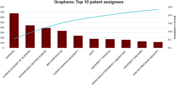
The importance of the US, China and South Korea is emphasised by the top assignees, shown in Fig. 14. The corporation with most graphene patent applications is the Korean multinational Samsung, with over three times as many filings as its nearest rival. It has also patented an unrivalled range of graphene-technology applications, including synthesis procedures,77 transparent display devices,78 composite materials,79 transistors,80 batteries and solar cells.81 Samsung’s patent applications indicate a sustained and heavy investment in graphene R&D, as well as collaboration (co-assignment of patents) with a wide range of academic institutions.82,83


image file: c4nr01600a-f14.tif
Fig. 14 Top 10 graphene patent assignees by number and cumulative over all time as of end-July 2014. Number of patents are indicated in the red histograms referred to the left Y axis, while the cumulative percentage is the blue line, referred to the right Y axis.

It is also interesting to note that patent filings by universities and research institutions make up a significant proportion ([similar]50%) of total patent filings: the other half comprises contributions from small and medium-sized enterprises (SMEs) and multinationals.
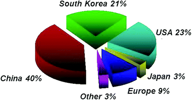
Europe’s position is shown in Fig. 10, 12 and 14. While Europe makes a good showing in the geographical distribution of publications, it lags behind in patent applications, with only 7% of patent filings as compared to 30% in the US, 25% in China, and 13% in South Korea (Fig. 13) and only 9% of filings by academic institutions assigned in Europe (Fig. 15).


image file: c4nr01600a-f15.tif
Fig. 15 Geographical breakdown of academic patent holders as of July 2014.

While Europe is trailing other regions in terms of number of patent filings, it nevertheless has a significant foothold in the patent landscape. Currently, the top European patent holder is Finland’s Nokia, primarily around incorporation of graphene into electrical devices, including resonators and electrodes.72,84,85

This may sound like Europe is trailing behind but that’s not the case according to the roadmap (Note: Links have been removed. Incidental numbers are footnote references),

European Universities also show promise in the graphene patent landscape. We also find evidence of corporate-academic collaborations in Europe, including e.g. co-assignments filed with European research institutions and Germany’s AMO GmbH,86 and chemical giant BASF.87,88 Finally, Europe sees significant patent filings from a number of international corporate and university players including Samsung,77 Vorbeck Materials,89 Princeton University,90–92 and Rice University,93–95 perhaps reflecting the quality of the European ST base around graphene, and its importance as a market for graphene technologies.

There are a number of features in the graphene patent landscape which may lead to a risk of patent thickets96 or ‘multiple overlapping granted patents’ existing around aspects of graphene technology systems. [emphasis mine] There is a relatively high volume of patent activity around graphene, which is an early stage technology space, with applications in patent intensive industry sectors. Often patents claim carbon nano structures other than graphene in graphene patent landscapes, illustrating difficulties around defining ‘graphene’ and mapping the graphene patent landscape. Additionally, the graphene patent nomenclature is not entirely settled. Different patent examiners might grant patents over the same components which the different experts and industry players call by different names.

For anyone new to this blog, I am not a big fan of current patent regimes as they seem to be stifling rather encouraging innovation. Sadly, patents and copyright were originally developed to encourage creativity and innovation by allowing the creators to profit from their ideas. Over time a system designed to encourage innovation has devolved into one that does the opposite. (My Oct. 31, 2011 post titled Patents as weapons and obstacles, details my take on this matter.) I’m not arguing against patents and copyright but suggesting that the system be fixed or replaced with something that delivers on the original intention.

Getting back to the matter at hand, here’s a link to and a citation for the 200 pp. 2015 European Graphene roadmap,

Science and technology roadmap for graphene, related two-dimensional crystals, and hybrid systems by Andrea C. Ferrari, Francesco Bonaccorso, Vladimir Fal’ko, Konstantin S. Novoselov, Stephan Roche, Peter Bøggild, Stefano Borini, Frank H. L. Koppens, Vincenzo Palermo, Nicola Pugno, José A. Garrido, Roman Sordan, Alberto Bianco, Laura Ballerini, Maurizio Prato, Elefterios Lidorikis, Jani Kivioja, Claudio Marinelli, Tapani Ryhänen, Alberto Morpurgo, Jonathan N. Coleman, Valeria Nicolosi, Luigi Colombo, Albert Fert, Mar Garcia-Hernandez, Adrian Bachtold, Grégory F. Schneider, Francisco Guinea, Cees Dekker, Matteo Barbone, Zhipei Sun, Costas Galiotis,  Alexander N. Grigorenko, Gerasimos Konstantatos, Andras Kis, Mikhail Katsnelson, Lieven Vandersypen, Annick Loiseau, Vittorio Morandi, Daniel Neumaier, Emanuele Treossi, Vittorio Pellegrini, Marco Polini, Alessandro Tredicucci, Gareth M. Williams, Byung Hee Hong, Jong-Hyun Ahn, Jong Min Kim, Herbert Zirath, Bart J. van Wees, Herre van der Zant, Luigi Occhipinti, Andrea Di Matteo, Ian A. Kinloch, Thomas Seyller, Etienne Quesnel, Xinliang Feng,  Ken Teo, Nalin Rupesinghe, Pertti Hakonen, Simon R. T. Neil, Quentin Tannock, Tomas Löfwander and Jari Kinaret. Nanoscale, 2015, Advance Article DOI: 10.1039/C4NR01600A First published online 22 Sep 2014

Here’s a diagram illustrating the roadmap process,

Fig. 122 The STRs [science and technology roadmaps] follow a hierarchical structure where the strategic level in a) is connected to the more detailed roadmap shown in b). These general roadmaps are the condensed form of the topical roadmaps presented in the previous sections, and give technological targets for key applications to become commercially competitive and the forecasts for when the targets are predicted to be met.  Courtesy: Researchers and  the Royal Society's journal, Nanoscale

Fig. 122 The STRs [science and technology roadmaps] follow a hierarchical structure where the strategic level in a) is connected to the more detailed roadmap shown in b). These general roadmaps are the condensed form of the topical roadmaps presented in the previous sections, and give technological targets for key applications to become commercially competitive and the forecasts for when the targets are predicted to be met.
Courtesy: Researchers and the Royal Society’s journal, Nanoscale

The image here is not the best quality; the one embedded in the relevant Nanowerk news item is better.

As for the earlier roadmap, here’s my Oct. 11, 2012 post on the topic.