Tag Archives: artificial neural networks

Graphene-based memristors for neuromorphic computing

An Oct. 29, 2020 news item on ScienceDaily features an explanation of the reasons for investigating brainlike (neuromorphic) computing ,

As progress in traditional computing slows, new forms of computing are coming to the forefront. At Penn State, a team of engineers is attempting to pioneer a type of computing that mimics the efficiency of the brain’s neural networks while exploiting the brain’s analog nature.

Modern computing is digital, made up of two states, on-off or one and zero. An analog computer, like the brain, has many possible states. It is the difference between flipping a light switch on or off and turning a dimmer switch to varying amounts of lighting.

Neuromorphic or brain-inspired computing has been studied for more than 40 years, according to Saptarshi Das, the team leader and Penn State [Pennsylvania State University] assistant professor of engineering science and mechanics. What’s new is that as the limits of digital computing have been reached, the need for high-speed image processing, for instance for self-driving cars, has grown. The rise of big data, which requires types of pattern recognition for which the brain architecture is particularly well suited, is another driver in the pursuit of neuromorphic computing.

“We have powerful computers, no doubt about that, the problem is you have to store the memory in one place and do the computing somewhere else,” Das said.

The shuttling of this data from memory to logic and back again takes a lot of energy and slows the speed of computing. In addition, this computer architecture requires a lot of space. If the computation and memory storage could be located in the same space, this bottleneck could be eliminated.

An Oct. 29, 2020 Penn State news release (also on EurekAlert), which originated the news item, describes what makes the research different,

“We are creating artificial neural networks, which seek to emulate the energy and area efficiencies of the brain,” explained Thomas Shranghamer, a doctoral student in the Das group and first author on a paper recently published in Nature Communications. “The brain is so compact it can fit on top of your shoulders, whereas a modern supercomputer takes up a space the size of two or three tennis courts.”

Like synapses connecting the neurons in the brain that can be reconfigured, the artificial neural networks the team is building can be reconfigured by applying a brief electric field to a sheet of graphene, the one-atomic-thick layer of carbon atoms. In this work they show at least 16 possible memory states, as opposed to the two in most oxide-based memristors, or memory resistors [emphasis mine].

“What we have shown is that we can control a large number of memory states with precision using simple graphene field effect transistors [emphasis mine],” Das said.

The team thinks that ramping up this technology to a commercial scale is feasible. With many of the largest semiconductor companies actively pursuing neuromorphic computing, Das believes they will find this work of interest.

Here’s a link to and a citation for the paper,

Graphene memristive synapses for high precision neuromorphic computing by Thomas F. Schranghamer, Aaryan Oberoi & Saptarshi Das. Nature Communications volume 11, Article number: 5474 (2020) DOI: https://doi.org/10.1038/s41467-020-19203-z Published: 29 October 2020

This paper is open access.

If only AI had a brain (a Wizard of Oz reference?)

The title, which I’ve borrowed from the news release, is the only Wizard of Oz reference that I can find but it works so well, you don’t really need anything more.

Moving onto the news, a July 23, 2018 news item on phys.org announces new work on developing an artificial synapse (Note: A link has been removed),

Digital computation has rendered nearly all forms of analog computation obsolete since as far back as the 1950s. However, there is one major exception that rivals the computational power of the most advanced digital devices: the human brain.

The human brain is a dense network of neurons. Each neuron is connected to tens of thousands of others, and they use synapses to fire information back and forth constantly. With each exchange, the brain modulates these connections to create efficient pathways in direct response to the surrounding environment. Digital computers live in a world of ones and zeros. They perform tasks sequentially, following each step of their algorithms in a fixed order.

A team of researchers from Pitt’s [University of Pittsburgh] Swanson School of Engineering have developed an “artificial synapse” that does not process information like a digital computer but rather mimics the analog way the human brain completes tasks. Led by Feng Xiong, assistant professor of electrical and computer engineering, the researchers published their results in the recent issue of the journal Advanced Materials (DOI: 10.1002/adma.201802353). His Pitt co-authors include Mohammad Sharbati (first author), Yanhao Du, Jorge Torres, Nolan Ardolino, and Minhee Yun.

A July 23, 2018 University of Pittsburgh Swanson School of Engineering news release (also on EurekAlert), which originated the news item, provides further information,

“The analog nature and massive parallelism of the brain are partly why humans can outperform even the most powerful computers when it comes to higher order cognitive functions such as voice recognition or pattern recognition in complex and varied data sets,” explains Dr. Xiong.

An emerging field called “neuromorphic computing” focuses on the design of computational hardware inspired by the human brain. Dr. Xiong and his team built graphene-based artificial synapses in a two-dimensional honeycomb configuration of carbon atoms. Graphene’s conductive properties allowed the researchers to finely tune its electrical conductance, which is the strength of the synaptic connection or the synaptic weight. The graphene synapse demonstrated excellent energy efficiency, just like biological synapses.

In the recent resurgence of artificial intelligence, computers can already replicate the brain in certain ways, but it takes about a dozen digital devices to mimic one analog synapse. The human brain has hundreds of trillions of synapses for transmitting information, so building a brain with digital devices is seemingly impossible, or at the very least, not scalable. Xiong Lab’s approach provides a possible route for the hardware implementation of large-scale artificial neural networks.

According to Dr. Xiong, artificial neural networks based on the current CMOS (complementary metal-oxide semiconductor) technology will always have limited functionality in terms of energy efficiency, scalability, and packing density. “It is really important we develop new device concepts for synaptic electronics that are analog in nature, energy-efficient, scalable, and suitable for large-scale integrations,” he says. “Our graphene synapse seems to check all the boxes on these requirements so far.”

With graphene’s inherent flexibility and excellent mechanical properties, these graphene-based neural networks can be employed in flexible and wearable electronics to enable computation at the “edge of the internet”–places where computing devices such as sensors make contact with the physical world.

“By empowering even a rudimentary level of intelligence in wearable electronics and sensors, we can track our health with smart sensors, provide preventive care and timely diagnostics, monitor plants growth and identify possible pest issues, and regulate and optimize the manufacturing process–significantly improving the overall productivity and quality of life in our society,” Dr. Xiong says.

The development of an artificial brain that functions like the analog human brain still requires a number of breakthroughs. Researchers need to find the right configurations to optimize these new artificial synapses. They will need to make them compatible with an array of other devices to form neural networks, and they will need to ensure that all of the artificial synapses in a large-scale neural network behave in the same exact manner. Despite the challenges, Dr. Xiong says he’s optimistic about the direction they’re headed.

“We are pretty excited about this progress since it can potentially lead to the energy-efficient, hardware implementation of neuromorphic computing, which is currently carried out in power-intensive GPU clusters. The low-power trait of our artificial synapse and its flexible nature make it a suitable candidate for any kind of A.I. device, which would revolutionize our lives, perhaps even more than the digital revolution we’ve seen over the past few decades,” Dr. Xiong says.

There is a visual representation of this artificial synapse,

Caption: Pitt engineers built a graphene-based artificial synapse in a two-dimensional, honeycomb configuration of carbon atoms that demonstrated excellent energy efficiency comparable to biological synapses Credit: Swanson School of Engineering

Here’s a link to and a citation for the paper,

Low‐Power, Electrochemically Tunable Graphene Synapses for Neuromorphic Computing by Mohammad Taghi Sharbati, Yanhao Du, Jorge Torres, Nolan D. Ardolino, Minhee Yun, Feng Xiong. Advanced Materials DOP: https://doi.org/10.1002/adma.201802353 First published [online]: 23 July 2018

This paper is behind a paywall.

I did look at the paper and if I understand it rightly, this approach is different from the memristor-based approaches that I have so often featured here. More than that I cannot say.

Finally, the Wizard of Oz song ‘If I Only Had a Brain’,

Brainy and brainy: a novel synaptic architecture and a neuromorphic computing platform called SpiNNaker

I have two items about brainlike computing. The first item hearkens back to memristors, a topic I have been following since 2008. (If you’re curious about the various twists and turns just enter  the term ‘memristor’ in this blog’s search engine.) The latest on memristors is from a team than includes IBM (US), École Politechnique Fédérale de Lausanne (EPFL; Swizterland), and the New Jersey Institute of Technology (NJIT; US). The second bit comes from a Jülich Research Centre team in Germany and concerns an approach to brain-like computing that does not include memristors.

Multi-memristive synapses

In the inexorable march to make computers function more like human brains (neuromorphic engineering/computing), an international team has announced its latest results in a July 10, 2018 news item on Nanowerk,

Two New Jersey Institute of Technology (NJIT) researchers, working with collaborators from the IBM Research Zurich Laboratory and the École Polytechnique Fédérale de Lausanne, have demonstrated a novel synaptic architecture that could lead to a new class of information processing systems inspired by the brain.

The findings are an important step toward building more energy-efficient computing systems that also are capable of learning and adaptation in the real world. …

A July 10, 2018 NJIT news release (also on EurekAlert) by Tracey Regan, which originated by the news item, adds more details,

The researchers, Bipin Rajendran, an associate professor of electrical and computer engineering, and S. R. Nandakumar, a graduate student in electrical engineering, have been developing brain-inspired computing systems that could be used for a wide range of big data applications.

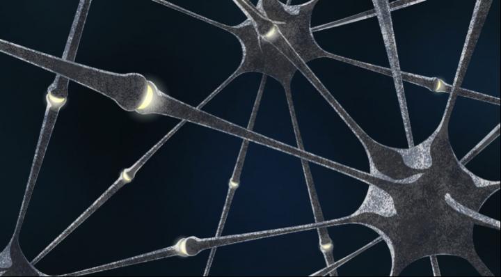
Over the past few years, deep learning algorithms have proven to be highly successful in solving complex cognitive tasks such as controlling self-driving cars and language understanding. At the heart of these algorithms are artificial neural networks – mathematical models of the neurons and synapses of the brain – that are fed huge amounts of data so that the synaptic strengths are autonomously adjusted to learn the intrinsic features and hidden correlations in these data streams.

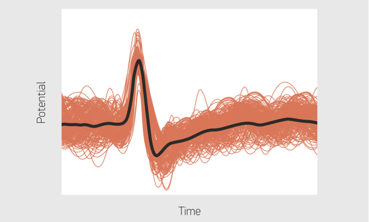
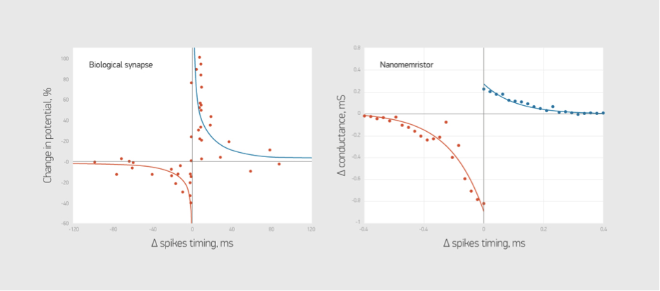
However, the implementation of these brain-inspired algorithms on conventional computers is highly inefficient, consuming huge amounts of power and time. This has prompted engineers to search for new materials and devices to build special-purpose computers that can incorporate the algorithms. Nanoscale memristive devices, electrical components whose conductivity depends approximately on prior signaling activity, can be used to represent the synaptic strength between the neurons in artificial neural networks.

While memristive devices could potentially lead to faster and more power-efficient computing systems, they are also plagued by several reliability issues that are common to nanoscale devices. Their efficiency stems from their ability to be programmed in an analog manner to store multiple bits of information; however, their electrical conductivities vary in a non-deterministic and non-linear fashion.

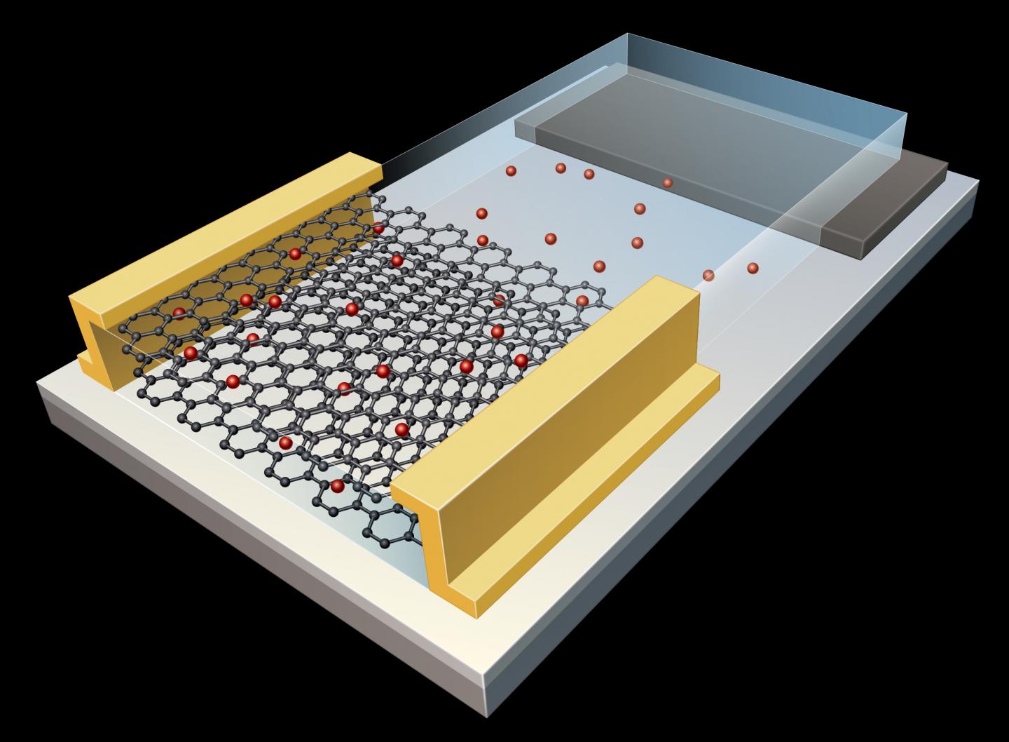
In the experiment, the team showed how multiple nanoscale memristive devices exhibiting these characteristics could nonetheless be configured to efficiently implement artificial intelligence algorithms such as deep learning. Prototype chips from IBM containing more than one million nanoscale phase-change memristive devices were used to implement a neural network for the detection of hidden patterns and correlations in time-varying signals.

“In this work, we proposed and experimentally demonstrated a scheme to obtain high learning efficiencies with nanoscale memristive devices for implementing learning algorithms,” Nandakumar says. “The central idea in our demonstration was to use several memristive devices in parallel to represent the strength of a synapse of a neural network, but only chose one of them to be updated at each step based on the neuronal activity.”

Here’s a link to and a citation for the paper,

Neuromorphic computing with multi-memristive synapses by Irem Boybat, Manuel Le Gallo, S. R. Nandakumar, Timoleon Moraitis, Thomas Parnell, Tomas Tuma, Bipin Rajendran, Yusuf Leblebici, Abu Sebastian, & Evangelos Eleftheriou. Nature Communications volume 9, Article number: 2514 (2018) DOI: https://doi.org/10.1038/s41467-018-04933-y Published 28 June 2018

This is an open access paper.

Also they’ve got a couple of very nice introductory paragraphs which I’m including here, (from the June 28, 2018 paper in Nature Communications; Note: Links have been removed),

The human brain with less than 20 W of power consumption offers a processing capability that exceeds the petaflops mark, and thus outperforms state-of-the-art supercomputers by several orders of magnitude in terms of energy efficiency and volume. Building ultra-low-power cognitive computing systems inspired by the operating principles of the brain is a promising avenue towards achieving such efficiency. Recently, deep learning has revolutionized the field of machine learning by providing human-like performance in areas, such as computer vision, speech recognition, and complex strategic games1. However, current hardware implementations of deep neural networks are still far from competing with biological neural systems in terms of real-time information-processing capabilities with comparable energy consumption.

One of the reasons for this inefficiency is that most neural networks are implemented on computing systems based on the conventional von Neumann architecture with separate memory and processing units. There are a few attempts to build custom neuromorphic hardware that is optimized to implement neural algorithms2,3,4,5. However, as these custom systems are typically based on conventional silicon complementary metal oxide semiconductor (CMOS) circuitry, the area efficiency of such hardware implementations will remain relatively low, especially if in situ learning and non-volatile synaptic behavior have to be incorporated. Recently, a new class of nanoscale devices has shown promise for realizing the synaptic dynamics in a compact and power-efficient manner. These memristive devices store information in their resistance/conductance states and exhibit conductivity modulation based on the programming history6,7,8,9. The central idea in building cognitive hardware based on memristive devices is to store the synaptic weights as their conductance states and to perform the associated computational tasks in place.

The two essential synaptic attributes that need to be emulated by memristive devices are the synaptic efficacy and plasticity. …

It gets more complicated from there.

Now onto the next bit.

SpiNNaker

At a guess, those capitalized N’s are meant to indicate ‘neural networks’. As best I can determine, SpiNNaker is not based on the memristor. Moving on, a July 11, 2018 news item on phys.org announces work from a team examining how neuromorphic hardware and neuromorphic software work together,

A computer built to mimic the brain’s neural networks produces similar results to that of the best brain-simulation supercomputer software currently used for neural-signaling research, finds a new study published in the open-access journal Frontiers in Neuroscience. Tested for accuracy, speed and energy efficiency, this custom-built computer named SpiNNaker, has the potential to overcome the speed and power consumption problems of conventional supercomputers. The aim is to advance our knowledge of neural processing in the brain, to include learning and disorders such as epilepsy and Alzheimer’s disease.

A July 11, 2018 Frontiers Publishing news release on EurekAlert, which originated the news item, expands on the latest work,

“SpiNNaker can support detailed biological models of the cortex–the outer layer of the brain that receives and processes information from the senses–delivering results very similar to those from an equivalent supercomputer software simulation,” says Dr. Sacha van Albada, lead author of this study and leader of the Theoretical Neuroanatomy group at the Jülich Research Centre, Germany. “The ability to run large-scale detailed neural networks quickly and at low power consumption will advance robotics research and facilitate studies on learning and brain disorders.”

The human brain is extremely complex, comprising 100 billion interconnected brain cells. We understand how individual neurons and their components behave and communicate with each other and on the larger scale, which areas of the brain are used for sensory perception, action and cognition. However, we know less about the translation of neural activity into behavior, such as turning thought into muscle movement.

Supercomputer software has helped by simulating the exchange of signals between neurons, but even the best software run on the fastest supercomputers to date can only simulate 1% of the human brain.

“It is presently unclear which computer architecture is best suited to study whole-brain networks efficiently. The European Human Brain Project and Jülich Research Centre have performed extensive research to identify the best strategy for this highly complex problem. Today’s supercomputers require several minutes to simulate one second of real time, so studies on processes like learning, which take hours and days in real time are currently out of reach.” explains Professor Markus Diesmann, co-author, head of the Computational and Systems Neuroscience department at the Jülich Research Centre.

He continues, “There is a huge gap between the energy consumption of the brain and today’s supercomputers. Neuromorphic (brain-inspired) computing allows us to investigate how close we can get to the energy efficiency of the brain using electronics.”

Developed over the past 15 years and based on the structure and function of the human brain, SpiNNaker — part of the Neuromorphic Computing Platform of the Human Brain Project — is a custom-built computer composed of half a million of simple computing elements controlled by its own software. The researchers compared the accuracy, speed and energy efficiency of SpiNNaker with that of NEST–a specialist supercomputer software currently in use for brain neuron-signaling research.

“The simulations run on NEST and SpiNNaker showed very similar results,” reports Steve Furber, co-author and Professor of Computer Engineering at the University of Manchester, UK. “This is the first time such a detailed simulation of the cortex has been run on SpiNNaker, or on any neuromorphic platform. SpiNNaker comprises 600 circuit boards incorporating over 500,000 small processors in total. The simulation described in this study used just six boards–1% of the total capability of the machine. The findings from our research will improve the software to reduce this to a single board.”

Van Albada shares her future aspirations for SpiNNaker, “We hope for increasingly large real-time simulations with these neuromorphic computing systems. In the Human Brain Project, we already work with neuroroboticists who hope to use them for robotic control.”

Before getting to the link and citation for the paper, here’s a description of SpiNNaker’s hardware from the ‘Spiking neural netowrk’ Wikipedia entry, Note: Links have been removed,

Neurogrid, built at Stanford University, is a board that can simulate spiking neural networks directly in hardware. SpiNNaker (Spiking Neural Network Architecture) [emphasis mine], designed at the University of Manchester, uses ARM processors as the building blocks of a massively parallel computing platform based on a six-layer thalamocortical model.[5]

Now for the link and citation,

Performance Comparison of the Digital Neuromorphic Hardware SpiNNaker and the Neural Network Simulation Software NEST for a Full-Scale Cortical Microcircuit Model by
Sacha J. van Albada, Andrew G. Rowley, Johanna Senk, Michael Hopkins, Maximilian Schmidt, Alan B. Stokes, David R. Lester, Markus Diesmann, and Steve B. Furber. Neurosci. 12:291. doi: 10.3389/fnins.2018.00291 Published: 23 May 2018

As noted earlier, this is an open access paper.

IBM to build brain-inspired AI supercomputing system equal to 64 million neurons for US Air Force

This is the second IBM computer announcement I’ve stumbled onto within the last 4 weeks or so,  which seems like a veritable deluge given the last time I wrote about IBM’s computing efforts was in an Oct. 8, 2015 posting about carbon nanotubes,. I believe that up until now that was my  most recent posting about IBM and computers.

Moving onto the news, here’s more from a June 23, 3017 news item on Nanotechnology Now,

IBM (NYSE: IBM) and the U.S. Air Force Research Laboratory (AFRL) today [June 23, 2017] announced they are collaborating on a first-of-a-kind brain-inspired supercomputing system powered by a 64-chip array of the IBM TrueNorth Neurosynaptic System. The scalable platform IBM is building for AFRL will feature an end-to-end software ecosystem designed to enable deep neural-network learning and information discovery. The system’s advanced pattern recognition and sensory processing power will be the equivalent of 64 million neurons and 16 billion synapses, while the processor component will consume the energy equivalent of a dim light bulb – a mere 10 watts to power.

A June 23, 2017 IBM news release, which originated the news item, describes the proposed collaboration, which is based on IBM’s TrueNorth brain-inspired chip architecture (see my Aug. 8, 2014 posting for more about TrueNorth),

IBM researchers believe the brain-inspired, neural network design of TrueNorth will be far more efficient for pattern recognition and integrated sensory processing than systems powered by conventional chips. AFRL is investigating applications of the system in embedded, mobile, autonomous settings where, today, size, weight and power (SWaP) are key limiting factors.

The IBM TrueNorth Neurosynaptic System can efficiently convert data (such as images, video, audio and text) from multiple, distributed sensors into symbols in real time. AFRL will combine this “right-brain” perception capability of the system with the “left-brain” symbol processing capabilities of conventional computer systems. The large scale of the system will enable both “data parallelism” where multiple data sources can be run in parallel against the same neural network and “model parallelism” where independent neural networks form an ensemble that can be run in parallel on the same data.

“AFRL was the earliest adopter of TrueNorth for converting data into decisions,” said Daniel S. Goddard, director, information directorate, U.S. Air Force Research Lab. “The new neurosynaptic system will be used to enable new computing capabilities important to AFRL’s mission to explore, prototype and demonstrate high-impact, game-changing technologies that enable the Air Force and the nation to maintain its superior technical advantage.”

“The evolution of the IBM TrueNorth Neurosynaptic System is a solid proof point in our quest to lead the industry in AI hardware innovation,” said Dharmendra S. Modha, IBM Fellow, chief scientist, brain-inspired computing, IBM Research – Almaden. “Over the last six years, IBM has expanded the number of neurons per system from 256 to more than 64 million – an 800 percent annual increase over six years.’’

The system fits in a 4U-high (7”) space in a standard server rack and eight such systems will enable the unprecedented scale of 512 million neurons per rack. A single processor in the system consists of 5.4 billion transistors organized into 4,096 neural cores creating an array of 1 million digital neurons that communicate with one another via 256 million electrical synapses.    For CIFAR-100 dataset, TrueNorth achieves near state-of-the-art accuracy, while running at >1,500 frames/s and using 200 mW (effectively >7,000 frames/s per Watt) – orders of magnitude lower speed and energy than a conventional computer running inference on the same neural network.

The IBM TrueNorth Neurosynaptic System was originally developed under the auspices of Defense Advanced Research Projects Agency’s (DARPA) Systems of Neuromorphic Adaptive Plastic Scalable Electronics (SyNAPSE) program in collaboration with Cornell University. In 2016, the TrueNorth Team received the inaugural Misha Mahowald Prize for Neuromorphic Engineering and TrueNorth was accepted into the Computer History Museum.  Research with TrueNorth is currently being performed by more than 40 universities, government labs, and industrial partners on five continents.

There is an IBM video accompanying this news release, which seems more promotional than informational,

The IBM scientist featured in the video has a Dec. 19, 2016 posting on an IBM research blog which provides context for this collaboration with AFRL,

2016 was a big year for brain-inspired computing. My team and I proved in our paper “Convolutional networks for fast, energy-efficient neuromorphic computing” that the value of this breakthrough is that it can perform neural network inference at unprecedented ultra-low energy consumption. Simply stated, our TrueNorth chip’s non-von Neumann architecture mimics the brain’s neural architecture — giving it unprecedented efficiency and scalability over today’s computers.

The brain-inspired TrueNorth processor [is] a 70mW reconfigurable silicon chip with 1 million neurons, 256 million synapses, and 4096 parallel and distributed neural cores. For systems, we present a scale-out system loosely coupling 16 single-chip boards and a scale-up system tightly integrating 16 chips in a 4´4 configuration by exploiting TrueNorth’s native tiling.

For the scale-up systems we summarize our approach to physical placement of neural network, to reduce intra- and inter-chip network traffic. The ecosystem is in use at over 30 universities and government / corporate labs. Our platform is a substrate for a spectrum of applications from mobile and embedded computing to cloud and supercomputers.
TrueNorth Ecosystem for Brain-Inspired Computing: Scalable Systems, Software, and Applications

TrueNorth, once loaded with a neural network model, can be used in real-time as a sensory streaming inference engine, performing rapid and accurate classifications while using minimal energy. TrueNorth’s 1 million neurons consume only 70 mW, which is like having a neurosynaptic supercomputer the size of a postage stamp that can run on a smartphone battery for a week.

Recently, in collaboration with Lawrence Livermore National Laboratory, U.S. Air Force Research Laboratory, and U.S. Army Research Laboratory, we published our fifth paper at IEEE’s prestigious Supercomputing 2016 conference that summarizes the results of the team’s 12.5-year journey (see the associated graphic) to unlock this value proposition. [keep scrolling for the graphic]

Applying the mind of a chip

Three of our partners, U.S. Army Research Lab, U.S. Air Force Research Lab and Lawrence Livermore National Lab, contributed sections to the Supercomputing paper each showcasing a different TrueNorth system, as summarized by my colleagues Jun Sawada, Brian Taba, Pallab Datta, and Ben Shaw:

U.S. Army Research Lab (ARL) prototyped a computational offloading scheme to illustrate how TrueNorth’s low power profile enables computation at the point of data collection. Using the single-chip NS1e board and an Android tablet, ARL researchers created a demonstration system that allows visitors to their lab to hand write arithmetic expressions on the tablet, with handwriting streamed to the NS1e for character recognition, and recognized characters sent back to the tablet for arithmetic calculation.

Of course, the point here is not to make a handwriting calculator, it is to show how TrueNorth’s low power and real time pattern recognition might be deployed at the point of data collection to reduce latency, complexity and transmission bandwidth, as well as back-end data storage requirements in distributed systems.

U.S. Air Force Research Lab (AFRL) contributed another prototype application utilizing a TrueNorth scale-out system to perform a data-parallel text extraction and recognition task. In this application, an image of a document is segmented into individual characters that are streamed to AFRL’s NS1e16 TrueNorth system for parallel character recognition. Classification results are then sent to an inference-based natural language model to reconstruct words and sentences. This system can process 16,000 characters per second! AFRL plans to implement the word and sentence inference algorithms on TrueNorth, as well.

Lawrence Livermore National Lab (LLNL) has a 16-chip NS16e scale-up system to explore the potential of post-von Neumann computation through larger neural models and more complex algorithms, enabled by the native tiling characteristics of the TrueNorth chip. For the Supercomputing paper, they contributed a single-chip application performing in-situ process monitoring in an additive manufacturing process. LLNL trained a TrueNorth network to recognize seven classes related to track weld quality in welds produced by a selective laser melting machine. Real-time weld quality determination allows for closed-loop process improvement and immediate rejection of defective parts. This is one of several applications LLNL is developing to showcase TrueNorth as a scalable platform for low-power, real-time inference.

[downloaded from https://www.ibm.com/blogs/research/2016/12/the-brains-architecture-efficiency-on-a-chip/] Courtesy: IBM

I gather this 2017 announcement is the latest milestone on the TrueNorth journey.

Deep learning and some history from the Swiss National Science Foundation (SNSF)

A June 27, 2016 news item on phys.org provides a measured analysis of deep learning and its current state of development (from a Swiss perspective),

In March 2016, the world Go champion Lee Sedol lost 1-4 against the artificial intelligence AlphaGo. For many, this was yet another defeat for humanity at the hands of the machines. Indeed, the success of the AlphaGo software was forged in an area of artificial intelligence that has seen huge progress over the last decade. Deep learning, as it’s called, uses artificial neural networks to process algorithmic calculations. This software architecture therefore mimics biological neural networks.

Much of the progress in deep learning is thanks to the work of Jürgen Schmidhuber, director of the IDSIA (Istituto Dalle Molle di Studi sull’Intelligenza Artificiale) which is located in the suburbs of Lugano. The IDSIA doctoral student Shane Legg and a group of former colleagues went on to found DeepMind, the startup acquired by Google in early 2014 for USD 500 million. The DeepMind algorithms eventually wound up in AlphaGo.

“Schmidhuber is one of the best at deep learning,” says Boi Faltings of the EPFL Artificial Intelligence Lab. “He never let go of the need to keep working at it.” According to Stéphane Marchand-Maillet of the University of Geneva computing department, “he’s been in the race since the very beginning.”

A June 27, 2016 SNSF news release (first published as a story in Horizons no. 109 June 2016) by Fabien Goubet, which originated the news item, goes on to provide a brief history,

The real strength of deep learning is structural recognition, and winning at Go is just an illustration of this, albeit a rather resounding one. Elsewhere, and for some years now, we have seen it applied to an entire spectrum of areas, such as visual and vocal recognition, online translation tools and smartphone personal assistants. One underlying principle of machine learning is that algorithms must first be trained using copious examples. Naturally, this has been helped by the deluge of user-generated content spawned by smartphones and web 2.0, stretching from Facebook photo comments to official translations published on the Internet. By feeding a machine thousands of accurately tagged images of cats, for example, it learns first to recognise those cats and later any image of a cat, including those it hasn’t been fed.

Deep learning isn’t new; it just needed modern computers to come of age. As far back as the early 1950s, biologists tried to lay out formal principles to explain the working of the brain’s cells. In 1956, the psychologist Frank Rosenblatt of the New York State Aeronautical Laboratory published a numerical model based on these concepts, thereby creating the very first artificial neural network. Once integrated into a calculator, it learned to recognise rudimentary images.

“This network only contained eight neurones organised in a single layer. It could only recognise simple characters”, says Claude Touzet of the Adaptive and Integrative Neuroscience Laboratory of Aix-Marseille University. “It wasn’t until 1985 that we saw the second generation of artificial neural networks featuring multiple layers and much greater performance”. This breakthrough was made simultaneously by three researchers: Yann LeCun in Paris, Geoffrey Hinton in Toronto and Terrence Sejnowski in Baltimore.

Byte-size learning

In multilayer networks, each layer learns to recognise the precise visual characteristics of a shape. The deeper the layer, the more abstract the characteristics. With cat photos, the first layer analyses pixel colour, and the following layer recognises the general form of the cat. This structural design can support calculations being made upon thousands of layers, and it was this aspect of the architecture that gave rise to the name ‘deep learning’.

Marchand-Maillet explains: “Each artificial neurone is assigned an input value, which it computes using a mathematical function, only firing if the output exceeds a pre-defined threshold”. In this way, it reproduces the behaviour of real neurones, which only fire and transmit information when the input signal (the potential difference across the entire neural circuit) reaches a certain level. In the artificial model, the results of a single layer are weighted, added up and then sent as the input signal to the following layer, which processes that input using different functions, and so on and so forth.

For example, if a system is trained with great quantities of photos of apples and watermelons, it will progressively learn to distinguish them on the basis of diameter, says Marchand-Maillet. If it cannot decide (e.g., when processing a picture of a tiny watermelon), the subsequent layers take over by analysing the colours or textures of the fruit in the photo, and so on. In this way, every step in the process further refines the assessment.

Video games to the rescue

For decades, the frontier of computing held back more complex applications, even at the cutting edge. Industry walked away, and deep learning only survived thanks to the video games sector, which eventually began producing graphics chips, or GPUs, with an unprecedented power at accessible prices: up to 6 teraflops (i.e., 6 trillion calculations per second) for a few hundred dollars. “There’s no doubt that it was this calculating power that laid the ground for the quantum leap in deep learning”, says Touzet. GPUs are also very good at parallel calculations, a useful function for executing the innumerable simultaneous operations required by neural networks.
Although image analysis is getting great results, things are more complicated for sequential data objects such as natural spoken language and video footage. This has formed part of Schmidhuber’s work since 1989, and his response has been to develop recurrent neural networks in which neurones communicate with each other in loops, feeding processed data back into the initial layers.

Such sequential data analysis is highly dependent on context and precursory data. In Lugano, networks have been instructed to memorise the order of a chain of events. Long Short Term Memory (LSTM) networks can distinguish ‘boat’ from ‘float’ by recalling the sound that preceded ‘oat’ (i.e., either ‘b’ or ‘fl’). “Recurrent neural networks are more powerful than other approaches such as the Hidden Markov models”, says Schmidhuber, who also notes that Google Voice integrated LSTMs in 2015. “With looped networks, the number of layers is potentially infinite”, says Faltings [?].

For Schmidhuber, deep learning is just one aspect of artificial intelligence; the real thing will lead to “the most important change in the history of our civilisation”. But Marchand-Maillet sees deep learning as “a bit of hype, leading us to believe that artificial intelligence can learn anything provided there’s data. But it’s still an open question as to whether deep learning can really be applied to every last domain”.

It’s nice to get an historical perspective and eye-opening to realize that scientists have been working on these concepts since the 1950s.

Memristor-based electronic synapses for neural networks

Caption: Neuron connections in biological neural networks. Credit: MIPT press office

Caption: Neuron connections in biological neural networks. Credit: MIPT press office

Russian scientists have recently published a paper about neural networks and electronic synapses based on ‘thin film’ memristors according to an April 19, 2016 news item on Nanowerk,

A team of scientists from the Moscow Institute of Physics and Technology (MIPT) have created prototypes of “electronic synapses” based on ultra-thin films of hafnium oxide (HfO2). These prototypes could potentially be used in fundamentally new computing systems.

An April 20, 2016 MIPT press release (also on EurekAlert), which originated the news item (the date inconsistency likely due to timezone differences) explains the connection between thin films and memristors,

The group of researchers from MIPT have made HfO2-based memristors measuring just 40×40 nm2. The nanostructures they built exhibit properties similar to biological synapses. Using newly developed technology, the memristors were integrated in matrices: in the future this technology may be used to design computers that function similar to biological neural networks.

Memristors (resistors with memory) are devices that are able to change their state (conductivity) depending on the charge passing through them, and they therefore have a memory of their “history”. In this study, the scientists used devices based on thin-film hafnium oxide, a material that is already used in the production of modern processors. This means that this new lab technology could, if required, easily be used in industrial processes.

“In a simpler version, memristors are promising binary non-volatile memory cells, in which information is written by switching the electric resistance – from high to low and back again. What we are trying to demonstrate are much more complex functions of memristors – that they behave similar to biological synapses,” said Yury Matveyev, the corresponding author of the paper, and senior researcher of MIPT’s Laboratory of Functional Materials and Devices for Nanoelectronics, commenting on the study.

The press release offers a description of biological synapses and their relationship to learning and memory,

A synapse is point of connection between neurons, the main function of which is to transmit a signal (a spike – a particular type of signal, see fig. 2) from one neuron to another. Each neuron may have thousands of synapses, i.e. connect with a large number of other neurons. This means that information can be processed in parallel, rather than sequentially (as in modern computers). This is the reason why “living” neural networks are so immensely effective both in terms of speed and energy consumption in solving large range of tasks, such as image / voice recognition, etc.

Over time, synapses may change their “weight”, i.e. their ability to transmit a signal. This property is believed to be the key to understanding the learning and memory functions of thebrain.

From the physical point of view, synaptic “memory” and “learning” in the brain can be interpreted as follows: the neural connection possesses a certain “conductivity”, which is determined by the previous “history” of signals that have passed through the connection. If a synapse transmits a signal from one neuron to another, we can say that it has high “conductivity”, and if it does not, we say it has low “conductivity”. However, synapses do not simply function in on/off mode; they can have any intermediate “weight” (intermediate conductivity value). Accordingly, if we want to simulate them using certain devices, these devices will also have to have analogous characteristics.

The researchers have provided an illustration of a biological synapse,

Fig.2 The type of electrical signal transmitted by neurons (a “spike”). The red lines are various other biological signals, the black line is the averaged signal. Source: MIPT press office

Fig.2 The type of electrical signal transmitted by neurons (a “spike”). The red lines are various other biological signals, the black line is the averaged signal. Source: MIPT press office

Now, the press release ties the memristor information together with the biological synapse information to describe the new work at the MIPT,

As in a biological synapse, the value of the electrical conductivity of a memristor is the result of its previous “life” – from the moment it was made.

There is a number of physical effects that can be exploited to design memristors. In this study, the authors used devices based on ultrathin-film hafnium oxide, which exhibit the effect of soft (reversible) electrical breakdown under an applied external electric field. Most often, these devices use only two different states encoding logic zero and one. However, in order to simulate biological synapses, a continuous spectrum of conductivities had to be used in the devices.

“The detailed physical mechanism behind the function of the memristors in question is still debated. However, the qualitative model is as follows: in the metal–ultrathin oxide–metal structure, charged point defects, such as vacancies of oxygen atoms, are formed and move around in the oxide layer when exposed to an electric field. It is these defects that are responsible for the reversible change in the conductivity of the oxide layer,” says the co-author of the paper and researcher of MIPT’s Laboratory of Functional Materials and Devices for Nanoelectronics, Sergey Zakharchenko.

The authors used the newly developed “analogue” memristors to model various learning mechanisms (“plasticity”) of biological synapses. In particular, this involved functions such as long-term potentiation (LTP) or long-term depression (LTD) of a connection between two neurons. It is generally accepted that these functions are the underlying mechanisms of  memory in the brain.

The authors also succeeded in demonstrating a more complex mechanism – spike-timing-dependent plasticity, i.e. the dependence of the value of the connection between neurons on the relative time taken for them to be “triggered”. It had previously been shown that this mechanism is responsible for associative learning – the ability of the brain to find connections between different events.

To demonstrate this function in their memristor devices, the authors purposefully used an electric signal which reproduced, as far as possible, the signals in living neurons, and they obtained a dependency very similar to those observed in living synapses (see fig. 3).

Fig.3. The change in conductivity of memristors depending on the temporal separation between "spikes"(rigth) and thr change in potential of the neuron connections in biological neural networks. Source: MIPT press office

Fig.3. The change in conductivity of memristors depending on the temporal separation between “spikes”(rigth) and thr change in potential of the neuron connections in biological neural networks. Source: MIPT press office

These results allowed the authors to confirm that the elements that they had developed could be considered a prototype of the “electronic synapse”, which could be used as a basis for the hardware implementation of artificial neural networks.

“We have created a baseline matrix of nanoscale memristors demonstrating the properties of biological synapses. Thanks to this research, we are now one step closer to building an artificial neural network. It may only be the very simplest of networks, but it is nevertheless a hardware prototype,” said the head of MIPT’s Laboratory of Functional Materials and Devices for Nanoelectronics, Andrey Zenkevich.

Here’s a link to and a citation for the paper,

Crossbar Nanoscale HfO2-Based Electronic Synapses by Yury Matveyev, Roman Kirtaev, Alena Fetisova, Sergey Zakharchenko, Dmitry Negrov and Andrey Zenkevich. Nanoscale Research Letters201611:147 DOI: 10.1186/s11671-016-1360-6

Published: 15 March 2016

This is an open access paper.