Tag Archives: atomic force microscope

Atomic force microscope (AFM) shrunk down to a dime-sized device?

Before getting to the announcement, here’s a little background from Dexter Johnson’s Feb. 21, 2017 posting on his NanoClast blog (on the IEEE [Institute of Electrical and Electronics Engineers] website; Note: Links have been removed),

Ever since the 1980s, when Gerd Binnig of IBM first heard that “beautiful noise” made by the tip of the first scanning tunneling microscope (STM) dragging across the surface of an atom, and he later developed the atomic force microscope (AFM), these microscopy tools have been the bedrock of nanotechnology research and development.

AFMs have continued to evolve over the years, and at one time, IBM even looked into using them as the basis of a memory technology in the company’s Millipede project. Despite all this development, AFMs have remained bulky and expensive devices, costing as much as $50,000 [or more].

Now, here’s the announcement in a Feb. 15, 2017 news item on Nanowerk,

Researchers at The University of Texas at Dallas have created an atomic force microscope on a chip, dramatically shrinking the size — and, hopefully, the price tag — of a high-tech device commonly used to characterize material properties.

“A standard atomic force microscope is a large, bulky instrument, with multiple control loops, electronics and amplifiers,” said Dr. Reza Moheimani, professor of mechanical engineering at UT Dallas. “We have managed to miniaturize all of the electromechanical components down onto a single small chip.”

A Feb. 15, 2017 University of Texas at Dallas news release, which originated the news item, provides more detail,

An atomic force microscope (AFM) is a scientific tool that is used to create detailed three-dimensional images of the surfaces of materials, down to the nanometer scale — that’s roughly on the scale of individual molecules.

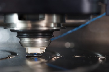
The basic AFM design consists of a tiny cantilever, or arm, that has a sharp tip attached to one end. As the apparatus scans back and forth across the surface of a sample, or the sample moves under it, the interactive forces between the sample and the tip cause the cantilever to move up and down as the tip follows the contours of the surface. Those movements are then translated into an image.

“An AFM is a microscope that ‘sees’ a surface kind of the way a visually impaired person might, by touching. You can get a resolution that is well beyond what an optical microscope can achieve,” said Moheimani, who holds the James Von Ehr Distinguished Chair in Science and Technology in the Erik Jonsson School of Engineering and Computer Science. “It can capture features that are very, very small.”

The UT Dallas team created its prototype on-chip AFM using a microelectromechanical systems (MEMS) approach.

“A classic example of MEMS technology are the accelerometers and gyroscopes found in smartphones,” said Dr. Anthony Fowler, a research scientist in Moheimani’s Laboratory for Dynamics and Control of Nanosystems and one of the article’s co-authors. “These used to be big, expensive, mechanical devices, but using MEMS technology, accelerometers have shrunk down onto a single chip, which can be manufactured for just a few dollars apiece.”

The MEMS-based AFM is about 1 square centimeter in size, or a little smaller than a dime. It is attached to a small printed circuit board, about half the size of a credit card, which contains circuitry, sensors and other miniaturized components that control the movement and other aspects of the device.

Conventional AFMs operate in various modes. Some map out a sample’s features by maintaining a constant force as the probe tip drags across the surface, while others do so by maintaining a constant distance between the two.

“The problem with using a constant height approach is that the tip is applying varying forces on a sample all the time, which can damage a sample that is very soft,” Fowler said. “Or, if you are scanning a very hard surface, you could wear down the tip,”

The MEMS-based AFM operates in “tapping mode,” which means the cantilever and tip oscillate up and down perpendicular to the sample, and the tip alternately contacts then lifts off from the surface. As the probe moves back and forth across a sample material, a feedback loop maintains the height of that oscillation, ultimately creating an image.

“In tapping mode, as the oscillating cantilever moves across the surface topography, the amplitude of the oscillation wants to change as it interacts with sample,” said Dr. Mohammad Maroufi, a research associate in mechanical engineering and co-author of the paper. “This device creates an image by maintaining the amplitude of oscillation.”

Because conventional AFMs require lasers and other large components to operate, their use can be limited. They’re also expensive.

“An educational version can cost about $30,000 or $40,000, and a laboratory-level AFM can run $500,000 or more,” Moheimani said. “Our MEMS approach to AFM design has the potential to significantly reduce the complexity and cost of the instrument.

“One of the attractive aspects about MEMS is that you can mass produce them, building hundreds or thousands of them in one shot, so the price of each chip would only be a few dollars. As a result, you might be able to offer the whole miniature AFM system for a few thousand dollars.”

A reduced size and price tag also could expand the AFMs’ utility beyond current scientific applications.

“For example, the semiconductor industry might benefit from these small devices, in particular companies that manufacture the silicon wafers from which computer chips are made,” Moheimani said. “With our technology, you might have an array of AFMs to characterize the wafer’s surface to find micro-faults before the product is shipped out.”

The lab prototype is a first-generation device, Moheimani said, and the group is already working on ways to improve and streamline the fabrication of the device.

“This is one of those technologies where, as they say, ‘If you build it, they will come.’ We anticipate finding many applications as the technology matures,” Moheimani said.

In addition to the UT Dallas researchers, Michael Ruppert, a visiting graduate student from the University of Newcastle in Australia, was a co-author of the journal article. Moheimani was Ruppert’s doctoral advisor.

So, an AFM that could cost as much as $500,000 for a laboratory has been shrunk to this size and become far less expensive,

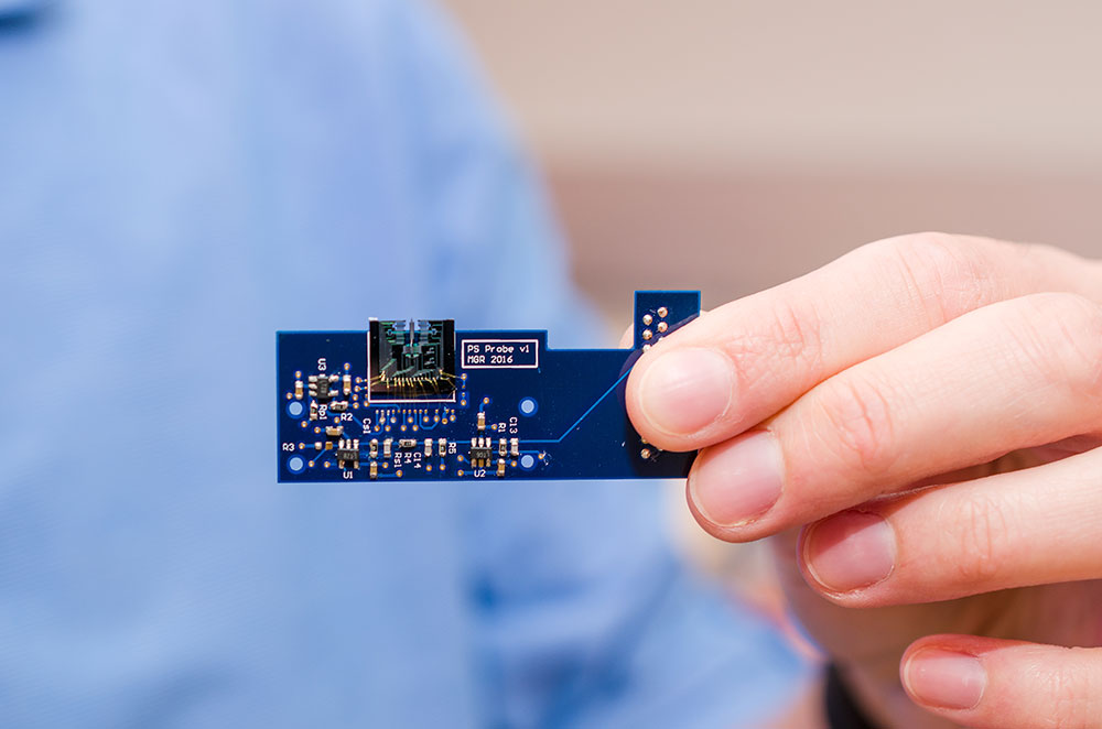
A MEMS-based atomic force microscope developed by engineers at UT Dallas is about 1 square centimeter in size (top center). Here it is attached to a small printed circuit board that contains circuitry, sensors and other miniaturized components that control the movement and other aspects of the device. Courtesy: University of Texas at Dallas

Of course, there’s still more work to be done as you’ll note when reading Dexter’s Feb. 21, 2017 posting where he features answers to questions he directed to the researchers.

Here’s a link to and a citation for the paper,

On-Chip Dynamic Mode Atomic Force Microscopy: A Silicon-on-Insulator MEMS Approach by  Michael G. Ruppert, Anthony G. Fowler, Mohammad Maroufi, S. O. Reza Moheimani. IEEE Journal of Microelectromechanical Systems Volume: 26 Issue: 1  Feb. 2017 DOI: 10.1109/JMEMS.2016.2628890 Date of Publication: 06 December 2016

This paper is behind a paywall.

All about Atomic Force Microscopy (AFM) with Gerd Binnig and Christoph Gerber

Gerd Binnig, Christoph Gerber, and Calvin Quate invented the atomic force microscope in the 1980s and an Aug. 16, 2016 news item on Nanotechnology Now announces a discussion with two of the inventors, Binnig and Gerber (Note: Links have been removed),

The inventors of one of the most versatile tools in modern science – the atomic force microscope, or AFM – tell their story in an interview published online this week. The AFM was invented in the mid 1980s by Gerd Binnig, Christoph Gerber and Calvin Quate, three physicists who are sharing the 2016 Kavli Prize in Nanoscience.

Binnig and Gerber discuss their inspiration for the device, how they solved problems through sport, and why their invention continues to propel science at the nanoscale.

This charming Aug. 20, 2016 discussion for the Kavli Foundation focuses on more than the AFM although it is the main topic,

Our roundtable panelists were:

GERD BINNIG –is a physicist and Nobel Laureate for his invention (with Heinrich Rohrer and Christoph Gerber) of the scanning tunneling microscope while at IBM Zurich. He began development of the atomic force microscope in 1986 to overcome the limitations of his previous invention.
CHRISTOPH GERBER –is a physicist and director for scientific communication at the Swiss Nanoscience Institute at the University of Basel. While at IBM, Gerber worked closely with Binnig on bringing both the scanning tunneling microscope and atomic force microscope to fruition.

Calvin Quate was unable to participate in the roundtable. The transcript has been amended and edited by the laureates

THE KAVLI FOUNDATION [TKF]: You filed your first patent for the atomic force microscope (AFM) nearly 30 years ago. How has it changed the way we look at the world since then?

GERD BINNIG: It was like the first time people looked through an optical microscope and saw bacteria. That completely changed how we look at the world. Suddenly, we understood what was really going on in nature, and we used that knowledge to learn how diseases spread. The AFM is the next step. It lets us look at the molecules that make life possible in those bacteria – and everywhere else – and see things we could not see before. It teaches us how to make changes to surfaces or molecules that we attempted blindly in the past. And it has been used in so many different scientific studies, from looking at polymers and chemical reactions to modifying surfaces at the atomic level.

CHRISTOPH GERBER: As Gerd explained, seeing is believing, and now we can do that onthe atomic scale. AFM has turned into the most powerful and most versatile toolkit that we have for doing nanoscience. And it keeps evolving. In just the past few years, researchers have learned to pick up a molecule on the tip of an AFM, which we can think of as the needle on a record player, and reveal chemical bonds while imaging molecules on surfaces. Nobody thought that ever would be possible.

TKF: Has this changed how researchers think about the ways nanoscale interactions affect the things they study?

BINNIG: Very much so. Before AFM, people who wanted to model very small structures –molecules, cell walls, semiconductors – had to make indirect measurements of them. But those structures can be complex and disordered, and indirect measurements do not always capture that, so the models they came up with were often wrong. But now, we can look at those structures and adapt our models to match what we observe. We as scientists always have to connect our theories to reality. Atomic force microscopy lets us do this.

TKF: When you started thinking about the AFM, biology was one of the fields you had inmind. Yet even you must have been surprised at how it has revolutionized biology.

GERBER: Yes. AFM’s capabilities keep evolving, and researchers are always finding new ways to use it. For example, in recent years, researchers have made tremendous progress in taking AFM measurements in real time. It’s like watching a movie. They can now see biological interactions, such as how molecules degrade or how antimicrobials attack bacterial membranes as they occur – something nobody could have foreseen 20 years ago. It took 15 years to get there, but we can now see biology in action and compare that to our theories.

BINNIG: Exactly. In biology, the biggest and most important question is always whether a molecule will bind to another molecule, change it, and by changing it cause something important to happen. This is all about forces, and researchers can use AFM to bring two molecules or even two cells close together, or pull them apart, and measure those forces directly. We can learn how big those forces are and under what conditions they occur. We’re actually looking into the heart of biology when we do that.

GERBER: And atomic force microscopy can tell us about many different types of forces that determine the outcome of chemical reactions at the nanoscale. These range from chemical, mechanical and electrostatic through, most recently, to the very weak interactions between molecules.

BINNIG: A great example of this is how Hermann Gaub, a professor of biophysics at Ludwig Maximilians University of Munich, used AFM to unfold proteins. He actually attached one end of a protein to a surface and the other end to an AFM tip. When he pulled the tip up, the protein straightened out and he could create a fingerprint of the unfolding forces that he could compare with his model.

TKF: What about applications you could not have foreseen?

BINNIG: I could not have foreseen that we can image molecules with such a high resolution. It’s unbelievable. We can see the bonds between molecules. We can watch them change during a chemical reaction, and sometimes there are surprises. Some researchers have observed an intermediate state in a chemical reaction that should not have lasted long enough to see. So they have had to rethink their theories to take into account why this intermediate state lasted so long. That’s what happens when we can observe such high-resolution details.

GERBER: Another example is high-speed AFM, which biologists use to see the cellular machinery in action. No other technique can do that. It works by tapping a very, very thin cantilever up and down, taking one quick measurement after another.

BINNIG: It is amazing how many people use the AFM in so many different fields. We first thought, well, maybe biology or semiconductor research. But it was picked up everywhere, from studying friction to cosmetics.

GERBER: I recently looked it up, and AFM was mentioned in 353,000 peer-reviewed papers. Our original article was published in Physical Review Letters, the top journal in the field in which all the important theoretical work is published. Ours is the only experimental paper on its list of most-cited papers.

TKF: Amazing. And yet AFM was actually a follow-up to another technology you worked on, the scanning tunneling microscope, or STM. It was probably the first instrument to achieve nanoscale resolution without using electrons or other high-energy beams that can damage what you are observing, right?

BINNIG: Yes.

TKF: And where did that idea come from?

BINNIG: We were trying to solve a problem. IBM was working on a new type of semiconductor chip, and the insulator, which keeps the electric current from escaping the semiconductor, was leaking. But no one knew why. So Heinrich Rohrer, who was working at IBM Zurich, hired me. I looked to all the available instruments, and none of them could study materials on such a fine scale to find out.

So the two of us thought, well, okay, we’ll invent something. We thought we could take advantage of something called quantum tunneling. Quantum tunneling is when an electron tunnels through a conducting material and come out the other side. We developed STM to map the surface of the material by measuring where electrons emerged on the other side. Only later did we realize that we could move our probe from one spot to cover the entire surface.

TKF: Dr. Gerber, you quickly became part of the STM team. What convinced you to join?

GERBER: I felt this was such a crazy idea, and I’m always very fond of this sort of thing. I thought this was fantastic.

BINNIG: I can confirm this. Christoph always likes crazy things. That runs through his life.

GERBER: Actually, the development of STM was kind of an undercover project at the beginning, because Gerd and Heinrich were involved in other projects. I worked for a year or so on my own. When we started overcoming problems and we could see features on the surface of a material that were one-tenth of a nanometer, then it really took off.

I leave you to discover the discussion in its entirety: Aug. 20, 2016 discussion.

Barnacle footprints could be useful

An Aug. 18, 2016 news item on Nanowerk describes efforts by scientists at the University of Twente (The Netherlands) and A*STAR (Singapore) to trace a barnacle’s footprints (Note: A link has been removed),

Barnacle’s larvae leave behind tiny protein traces on a ship hull: but what is the type of protein and what is the protein-surface interaction? Conventional techniques can only identify dissolved proteins, and in large quantities. Using a modified type of an Atomic Force Microscope, scientists of the University of Twente in The Netherlands and A*STAR in Singapore, can now measure protein characteristics of even very small traces on a surface. They present the new technique in Nature Nanotechnology (“Measuring protein isoelectric points by AFM-based force spectroscopy using trace amounts of sample”).

An Aug. 16, 2016 University of Twente press release, which originated the news item, explains how the ‘footprints’ could lead to new applications for ships and boats and briefly describes the technical aspects of the research,

In infection diseases, membrane fouling, interaction with bacteria, as well as in rapid healing of wounds for example, the way proteins interact with a surface plays an important role. On a surface, they function in a different way than in solution. On a ship hull, the larvae of the barnacle will leave tiny traces of protein to test if the surface is attractive for long-term attachment. If we get to know more about this interaction, it will be possible to develop surface conditions that are less attractive for the barnacle. Large amounts of barnacles on a ship will have a destructive effect on flow resistance and will lead to more fuel consumption. The new measuring method makes use of a modified Atomic Force Microscope: a tiny ball glued to the cantilever of the microscope will attract protein molecules.

Modified AFM tip with a tiny ball that can attract protein molecules

FORCE MEASUREMENTS

An amount of just hundreds of protein molecules will be sufficient to determine a crucial value, called the iso-electric point (pI): this is the pH-value at which the protein has net zero electric charge. The pI value says a lot about the surroundings a protein will ‘feel comfortable’ in, and to which it preferably moves. Using the AFM microscope, of which the modified tip has collected protein molecules, it is possible to perform force measurements for different pH values. The tip will be attracted or repelled, or show no movement when the pI point is reached. For these measurement, the researchers made a special reference material consisting of several layers. Using this, the effect of a number of pH-values can be tested until the pI value is found.

The traces the larve leaves behind (left) and force measurements (right)

PAINT CHANGE

The tests have been successfully performed for a number of known proteins like fibrinogen, myoglobine and bovine albumin. And returning to the barnacle: the tiny protein footprint will contain enough molecules to determine the pI value. This quantifies the ideal surface conditions, and using this knowledge, new choices can be made for e.g. the paint that is used on a ship hull.

The research has been done within the group Materials Science and Technology of Polymers of Professor Julius Vancso, in close collaboration with colleagues of A*STAR in Singapore – Prof Vancso is a Visiting Professor there as well. His group is part of UT’s MESA+ Institute for Nanotechnology.

Here’s a link to and a citation for the paper,

Measuring protein isoelectric points by AFM-based force spectroscopy using trace amounts of sample by Shifeng Gu, Xiaoying Zhu, Dominik Jańczewski, Serina Siew Chen Lee, Tao He, Serena Lay Ming Teo, & G. Julius Vancso.  Nature Nanotechnology (2016) doi:10.1038/nnano.2016.118 Published online 25 July 2016

This paper is behind a paywall.

Nature celebrates some nanotechnology anniversaries

An April 5, 2016 editorial in Nature magazine celebrates some nanotechnology milestones (Note: Links have been removed),

In March 1986, the atomic force microscope (AFM) was introduced by Gerd Binnig, Calvin Quate and Christoph Gerber with a paper in the journal Physical Review Letters titled simply ‘Atomic force microscope’1. This was 5 years (to the month) after the precursor to the AFM, the scanning tunnelling microscope (STM), had first been successfully tested at IBM’s Zurich Research Laboratory by Binnig and the late Heinrich Rohrer, and 7 months before Binnig and Rohrer were awarded a share of the Nobel Prize in Physics for the design of the STM (the prize was shared with Ernst Ruska, the inventor of the electron microscope). Achieving atomic resolution with the AFM proved more difficult than with the STM. It was, for example, only two years after its invention that the STM provided atomic-resolution images of an icon of surface science, the 7 × 7 surface reconstruction of Si(111) (ref. 2), whereas it took 8 years to achieve a similar feat with the AFM3, 4.

The editorial also provides an explanation of how the AFM works,

The AFM works by scanning a sharp tip attached to a flexible cantilever across a sample while measuring the interaction between the tip and the sample surface. The technique can operate in a range of environments, including in liquid and in air, and unlike the STM, it can be used with insulating materials; in their original paper, Binnig and colleagues used the instrument to analyse an aluminium oxide sample.

Then, the editorial touches on DNA (deoxyribonucleic acid) nanotechnology (Note: Links have been removed),

The history of structural DNA nanotechnology can, like the AFM, be traced back to the early 1980s, when Nadrian Seeman suggested that the exquisite base-pairing rules of DNA could be exploited to build artificial self-assembled structures11. But the founding experiment of the field came later. In April 1991, Seeman and Junghuei Chen reported building a cube-like molecular complex from DNA using a combination of branched junctions and single-stranded ‘sticky’ ends12. A range of significant advances soon followed, from 2D DNA arrays to DNA-based nanomechanical devices.

Then, in March 2006, the field of structural DNA nanotechnology experienced another decisive moment: Paul Rothemund reported the development of DNA origami13. This technique involves folding a long single strand of DNA into a predetermined shape with the help of short ‘staple’ strands. Used at first to create 2D structures, which were incidentally characterized using the AFM, the approach was quickly expanded to the building of intricate 3D structures and the organization of other species such as nanoparticles and proteins. …

Happy reading!

Developing optical microscopes that measure features down to 10 nanometer level on computer chips

The US National Institute of Standards and Technology (NIST) issued a Dec. 2, 2015 news release (also on EurekAlert) announcing a new kind of optical microscope and its possible impact on the semiconductor industry,

National Institute of Standards and Technology (NIST) researchers are seeing the light, but in an altogether different way. And how they are doing it just might be the semiconductor industry’s ticket for extending its use of optical microscopes to measure computer chip features that are approaching 10 nanometers, tiny fractions of the wavelength of light.

The news release goes on to provide details and an explanation of scatterfield imaging,

Using a novel microscope that combines standard through-the-lens viewing with a technique called scatterfield imaging, the NIST team accurately measured patterned features on a silicon wafer that were 30 times smaller than the wavelength of light (450 nanometers) used to examine them. They report* that measurements of the etched lines–as thin as 16 nanometers wide–on the SEMATECH-fabricated wafer were accurate to one nanometer. With the technique, they spotted variations in feature dimensions amounting to differences of a few atoms.

Measurements were confirmed by those made with an atomic force microscope, which achieves sub-nanometer resolution, but is considered too slow for online quality-control measurements. Combined with earlier results, the NIST researchers write, the new proof-of-concept study* suggests that the innovative optical approach could be a “realistic solution to a very challenging problem” facing chip makers and others aiming to harness advances in nanotechnology. All need the means for “nondestructive measurement of nanometer-scale structures with sub-nanometer sensitivity while still having high throughput.

“Light-based, or optical, microscopes can’t “see” features smaller than the wavelength of light, at least not in the crisp detail necessary for making accurate measurements. However, light does scatter when it strikes so-called subwavelength features and patterned arrangements of such features. “Historically, we would ignore this scattered light because it did not yield sufficient resolution,” explains Richard Silver, the physicist who initiated NIST’s scatterfield imaging effort. “Now we know it contains helpful information that provides signatures telling us something about where the light came from.”

With scatterfield imaging, Silver and colleagues methodically illuminate a sample with polarized light from different angles. From this collection of scattered light–nothing more than a sea of wiggly lines to the untrained eye–the NIST team can extract characteristics of the bounced lightwaves that, together, reveal the geometry of features on the specimen.

Light-scattering data are gathered in slices, which together image the volume of scattered light above and into the sample. These slices are analyzed and reconstructed to create a three-dimensional representation. The process is akin to a CT scan, except that the slices are collections of interfering waves, not cross-sectional pictures.

“It’s the ensemble of data that tells us what we’re after,” says project leader Bryan Barnes.” We may not be able see the lines on the wafer, but we can tell you what you need to know about them–their size, their shape, their spacing.”

Scatterfield imaging has critical prerequisites that must be met before it can yield useful data for high-accuracy measurements of exceedingly small features. Key steps entail detailed evaluation of the path light takes as it beams through lenses, apertures and other system elements before reaching the sample. The path traversed by light scattering from the specimen undergoes the same level of scrutiny. Fortunately, scatterfield imaging lends itself to thorough characterization of both sequences of optical devices, according to the researchers. These preliminary steps are akin to error mapping so that recognized sources of inaccuracy are factored out of the data.

The method also benefits from a little advance intelligence–the as-designed arrangement of circuit lines on a chip, down to the size of individual features. Knowing what is expected to be the result of the complex chip-making process sets up a classic matchup of theory vs. experiment.

The NIST researchers can use standard equations to simulate light scattering from an ideal, defect-free pattern and, in fact, any variation thereof. Using wave analysis software they developed, the team has assembled an indexed library of light-scattering reference models. So once a specimen is scanned, the team relies on computers to compare their real-world data to models and to find close matches.

From there, succeeding rounds of analysis homes in on the remaining differences, reducing them until the only ones that remain are due to variations in geometry such as irregularities in the height, width, or shape of a line.

Measurement results achieved with the NIST approach might be said to cast light itself in an entirely new light. Their new study, the researchers say, shows that once disregarded scattered light “contains a wealth of accessible optical information.”

Next steps include extending the technique to even shorter wavelengths of light, down to ultraviolet, or 193 nanometers. The aim is to accurately measure features as small as 5 nanometers.

This work is part of a larger NIST effort to supply measurement tools that enable the semiconductor industry to continue doubling the number of devices on a chip about every two years and to help other industries make products with nanoscale features. Recently, NIST and Intel researchers reported using an X-ray technique to accurately measure features on a silicon chip to within fractions of a nanometer.

Here’s a link to and a citation for a PDF of the paper,

Deep-subwavelength Nanometric Image Reconstruction using Fourier Domain Optical Normalization by Jing  Qin, Richard  M Silver, Bryan  M  Barnes, Hui Zhou, Ronald G Dixson, and Mark Alexander Hen. Light: Science & Applications accepted article preview 5 November 2015; e16038 doi: 10.1038/lsa.2016.38

[Note:] This is a PDF file of an unedited peer-reviewed manuscript that has been accepted for publication. NPG are providing this early version of the manuscript as a service to our customers. The manuscript will undergo copy editing, typesetting and a proof review before it is published in its final form. Please note that during the production process errors may be discovered which could affect the content, and all legal disclaimers apply.

This seems to be an open access paper but it is an early version.

Mini Lisa made possible by ThermoChemical NanoLithography

One of the world’s most recognizable images has undergone a makeover of sorts. According to an Aug. 6, 2013 news item on Azonano, researchers Georgia institute of Technology (Georgia Tech) in the US, have created a mini Mona Lisa,

The world’s most famous painting has now been created on the world’s smallest canvas. Researchers at the Georgia Institute of Technology have “painted” the Mona Lisa on a substrate surface approximately 30 microns in width – or one-third the width of a human hair.

The team’s creation, the “Mini Lisa,” demonstrates a technique that could potentially be used to achieve nanomanufacturing of devices because the team was able to vary the surface concentration of molecules on such short-length scales.

The Aug. 5, 2013 Georgia Tech news release, which originated the news item, provides more technical details,

The image was created with an atomic force microscope and a process called ThermoChemical NanoLithography (TCNL). Going pixel by pixel, the Georgia Tech team positioned a heated cantilever at the substrate surface to create a series of confined nanoscale chemical reactions. By varying only the heat at each location, Ph.D. Candidate Keith Carroll controlled the number of new molecules that were created. The greater the heat, the greater the local concentration. More heat produced the lighter shades of gray, as seen on the Mini Lisa’s forehead and hands. Less heat produced the darker shades in her dress and hair seen when the molecular canvas is visualized using fluorescent dye. Each pixel is spaced by 125 nanometers.

“By tuning the temperature, our team manipulated chemical reactions to yield variations in the molecular concentrations on the nanoscale,” said Jennifer Curtis, an associate professor in the School of Physics and the study’s lead author. “The spatial confinement of these reactions provides the precision required to generate complex chemical images like the Mini Lisa.”

Production of chemical concentration gradients and variations on the sub-micrometer scale are difficult to achieve with other techniques, despite a wide range of applications the process could allow. The Georgia Tech TCNL research collaboration, which includes associate professor Elisa Riedo and Regents Professor Seth Marder, produced chemical gradients of amine groups, but expects that the process could be extended for use with other materials.

“We envision TCNL will be capable of patterning gradients of other physical or chemical properties, such as conductivity of graphene,” Curtis said. “This technique should enable a wide range of previously inaccessible experiments and applications in fields as diverse as nanoelectronics, optoelectronics and bioengineering.”

Another advantage, according to Curtis, is that atomic force microscopes are fairly common and the thermal control is relatively straightforward, making the approach accessible to both academic and industrial laboratories.  To facilitate their vision of nano-manufacturing devices with TCNL, the Georgia Tech team has recently integrated nanoarrays of five thermal cantilevers to accelerate the pace of production. Because the technique provides high spatial resolutions at a speed faster than other existing methods, even with a single cantilever, Curtis is hopeful that TCNL will provide the option of nanoscale printing integrated with the fabrication of large quantities of surfaces or everyday materials whose dimensions are more than one billion times larger than the TCNL features themselves.

Here’s an image of the AFM and the cantilever used in the TCNL process to create the ‘Mini Lisa’,

Atomic force microscope (AFM) modified with a thermal cantilever. The AFM scanner allows for precise positioning on the nanoscale while the thermal cantilever induces local nanoscale chemical reactions. Courtesy Georgia Tech

Atomic force microscope (AFM) modified with a thermal cantilever. The AFM scanner allows for precise positioning on the nanoscale while the thermal cantilever induces local nanoscale chemical reactions. Courtesy Georgia Tech

Finally, the “Mini Lisa’,

Georgia Tech researchers have created the "Mini Lisa" on a substrate surface approximately 30 microns in width. The image demonstrates a technique that could potentially be used to achieve nano-manufacturing of devices because the team was able to vary the surface concentration of molecules on such short length scales. Courtesy Georgia Tech

Georgia Tech researchers have created the “Mini Lisa” on a substrate surface approximately 30 microns in width. The image demonstrates a technique that could potentially be used to achieve nano-manufacturing of devices because the team was able to vary the surface concentration of molecules on such short length scales. Courtesy Georgia Tech

For those who can’t get enough of the ‘Mini Lisa’ or TCNL, here’s a link to and a citation for the research team’s published paper,

Fabricating Nanoscale Chemical Gradients with ThermoChemical NanoLithography by Keith M. Carroll, Anthony J. Giordano, Debin Wang, Vamsi K. Kodali, Jan Scrimgeour, William P. King, Seth R. Marder, Elisa Riedo, and Jennifer E. Curtis. Langmuir, 2013, 29 (27), pp 8675–8682 DOI: 10.1021/la400996w Publication Date (Web): June 10, 2013
Copyright © 2013 American Chemical Society

This article is behind a paywall.

All about the University of Calgary and its microscopy and imaging facility

A July 24, 2012 news item on Nanowerk features the the equipment and capabilities of …

The Calgary Microscopy and Imaging Facility (MIF) is a world-class university-wide facility housing transmission electron microscopy (TEM), scanning electron microscopy (SEM), advanced light microscopy, atomic force microscopy (AFM), including single cell force spectroscopy (SCFS), and advanced image processing for three-dimensional electron and light microscopy, directed by Professor Matthias Amrein.

Single cell force spectroscopy at the MIF has now attracted high profile research with three NanoWizard® AFM systems from JPK [Instruments], one of which is equipped with the CellHesion® module. Describing the work of the Calgary group, Professor Amrein says “While we do some work for the energy sector (to predict behaviour of nanoparticles injected into oil reservoirs) our main focus is medicine. We delve into very fundamental problems such as “how does a malaria red blood cell attach itself to a blood vessel” or “how does binding of a ligand to a cell surface receptor or contact of a crystalline surface with the plasma membrane drive lipid sorting and how will this lead to signalling” but then immediately apply it to a practical problem such as “how does contact of uric acid crystals with dendritic cells cause gout in affected joints and how can we prevent this occurrence?” We want to understand disease processes at a very fundamental level so we know how to intervene in the best possible way. For example, a chronic inflammatory disease such as gout or arteriosclerosis may be triggered by a very specific interaction of a particle (uric acid crystals, cholesterol crystals, amyloid plaque, …. ) and specific cell (dendritic cell, macrophage, T-cell, …). Understanding this interaction will lead to targeted treatment “block the interaction” rather than the non-specific dampening of inflammation such as by corticosteroids with its many well-documented side effects and limited efficacy.”

It’s always nice to get some information about activities in microscopy, etc. in Canada although I’m not sure what occasioned the news item/release.

Canada’s Spectra Research gets exclusive distribution rights for super duper Asylum research microscopes

It’s all about microscopes, scanning probe and atomic force microscopes, that is. Asylum Research, a US company that recently (May 29, 2012)  announced the world’s first five year instrument warranty for atomic force microscopes, has appointed Canada’s Spectra Research Corporation as an exclusive distributor for Asylum’s microscopy products (and their other scientific instrumentation). From the June 6, 2012 news item on Nanowerk,

As part of its ongoing expansion, Asylum Research, the technology leader in scanning probe and atomic force microscopy (SPM/AFM), announced today that it has appointed Spectra Research Corporation (SRC) as its exclusive distributor in Canada. SRC has served nanotechnology and surface science markets in Canada since 1993. …

“We are very excited about adding Spectra Research to our family of world-wide distributors,” said John Green, Executive Vice President of Sales for Asylum Research. “Their extensive experience in AFM, materials and life science, and scientific instrumentation, will be a great asset to Asylum Research and our ability to help prospective customers make informed decisions.”

Paul Greenwood, President of SRC, added, “… This addition is a good fit with our focus on Canadian markets that include nanotech, surface science and materials characterization”.

SRC, located in Mississauga, Ontario, is one of the Allan Crawford Associates (ACA) group of companies. Neither SRC nor ACA offer much informaton about themselves or products on their websites. As for Asylum Research, you can find this on their About page,

Asylum Research is the technology leader in atomic force and scanning probe microscopy (AFM/SPM) for both materials and bioscience applications.  Founded in 1999, we are an employee owned company dedicated to innovative instrumentation for nanoscience and nanotechnology, with over 250 years combined AFM/SPM experience among our staff. Our instruments are used for a variety of nanoscience applications in material science, physics, polymers, chemistry, biomaterials, and bioscience, including single molecule mechanical experiments on DNA, protein unfolding and polymer elasticity, as well as force measurements for biomaterials, chemical sensing, polymers, colloidal forces, adhesion, and more.
Asylum’s MFP-3D set the standard for AFM technology, with unprecedented precision and flexibility. The MFP-3D is the first AFM with true independent piezo positioning in all three axes, combined with low noise closed-loop feedback sensor technology. The MFP-3D offers both top and bottom sample viewing and easy integration with most commercially-available inverted optical microscopes.

Asylum’s new Cypher AFM sets the new standard as the world’s fastest and highest resolution AFM.  Cypher provides low-drift closed loop atomic resolution for the most accurate images and measurements possible today, point defect atomic resolution, >20X faster AC imaging with small cantilevers, Spot-On™ automated laser and photodetector alignment for easy setup, integrated thermal, acoustic and vibration control, and broad support for all major AFM/SPM scanning modes and capabilities.

Asylum Research offers the lowest cost of ownership of any AFM company. Ask us about our industry-best 5-year warranty, our legendary product and applications support, and our exclusive 6-month money-back satisfaction guarantee. We are dedicated to providing the most technically advanced AFMs for researchers who want to take their experiments to the next level.

There’s a lot more information about their products and services on Asylum Research’s website.