Tag Archives: atomic layer deposition

Toughening up your electronics: kevlar with a tungsten fibre coating

An upcoming presentation at the 61st annual AVS Conference (Nov. 9 – 14, 2014) features a fibre made of tungsten that when added to kevlar offers the possibility of ‘tough’ electronics. From an Oct. 31, 2014 news item on Nanowerk (Note: A link has been removed),

A group of North Carolina State University researchers is exploring novel ways to apply semiconductor industry processes to unique substrates, such as textiles and fabrics, to “weave together” multifunctional materials with distinct capabilities.

During the AVS 61st International Symposium & Exhibition, being held November 9-14, 2014, in Baltimore, Maryland, the researchers will describe how they were able to “weave” high-strength, highly conductive yarns made of tungsten metal on Kevlar — aka body armor material — by using atomic layer deposition (ALD), a process commonly used for producing memory and logic devices.

An Oct. 28, 2014 AVS: Science & Technology of Materials, Interfaces, and Processing news release on Newswire, which originated the news item provides more details about this multifunctional material and a good description of atomic layer deposition (ALD),

“As a substrate, Kevlar was intriguing to us because it’s capable of withstanding the relatively high temperature (220°C) required by the ALD deposition process,” explains Sarah Atanasov, a Ph.D. candidate in the Biomolecular Engineering Department at North Carolina State University. “Kevlar doesn’t begin to degrade until it reaches nearly 400°C.”

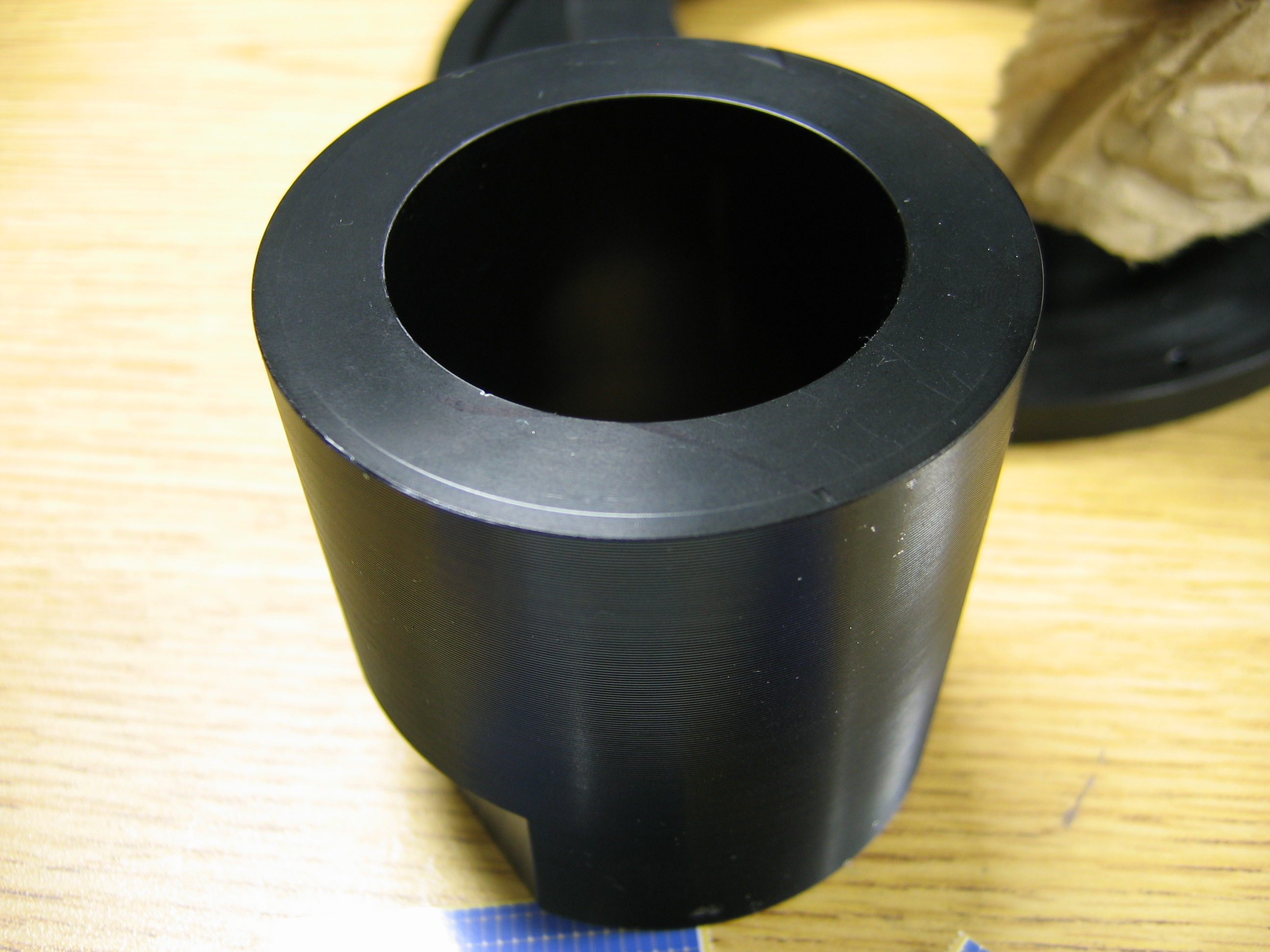
The group selected ALD as a process because it allows them to deposit highly conformal films on nonplanar surfaces with nanometer-thickness precision. “This ensures that the entire surface of the yarn — made of nearly 600 fibers, each 12 microns in diameter — is evenly coated,” said Atanasov.

How does the ALD process work? It’s actually a cyclical process, which begins by exposing the substrate’s surface to one gas-phase chemical, in this case tungsten hexafluoride (WF6), followed by removal of any unreacted material. This is chased with surface exposure to a second gas-phase chemical, silane (SiH4), after which any unreacted material is once again removed.

By the end of the ALD cycle, the two chemicals have reacted to produce tungsten. “This is a self-limited process, meaning that a single atomic layer is deposited during each cycle — in this case ~5.5 Angstroms per cycle,” Atanasov said. “The process can be cycled through a number of times to achieve any specifically desired thickness. As a bonus, ALD occurs in the gas phase, so it doesn’t require any solution processing and is considered to be a more sustainable deposition technique.”

While weaving together multiple fabrics to combine multiple capabilities certainly isn’t new, characteristics such as high strength, high conductivity, and flexibility are frequently regarded as being mutually exclusive — so concessions are often made to get the most important one.

The work by Atanasov and colleagues shows, however, that ALD of tungsten on Kevlar yields yarns that are highly flexible and highly conductive, around 2,000 S/cm (“Siemens per centimeter,” a common unit used for conductivity). The yards are also within 90 percent of their original prior-to-coating tensile strength.

“Introducing well-established processes from one area into a completely new field can lead to some very interesting and useful results,” Atanasov noted.

The group’s tungsten-on-Kevlar yarns are expected to find applications in multifunctional protective electronics materials for electromagnetic shielding and communications, as well as erosion-resistant antistatic fabrics for space and automated technologies.

Presentation #MS+PS+TF-ThA4, “Multifunctional Fabrics via Tungsten ALD on Kevlar,” authored by Sarah Atanasov, B. Kalanyan and G.N. Parsons, will be at 3:20 p.m. ET on Thursday, Nov. 13, 2014.

Atanasov recently published a paper about another kevlar project where she worked to enhance its ‘stab resistance’ with a titanium dioxide/aluminum mixture as Anisha Ratan notes in her Sept. 12, 2014 article (Oxide armour offers Kevlar better stab resistance)  (excerpt from Ratan’s article for the Royal Society; Note: Links have been removed),

Scientists in the US have synthesised an ultrathin inorganic bilayer coating for Kevlar that could improve its stab resistance by 30% and prove invaluable for military and first-responders requiring multi-threat protection clothes.

Developed in 1965 by Stephanie Kwolek at DuPont, poly(p-phenylene terephthalamide) (PPTA), or Kevlar, is a para-aramid synthetic fiber deriving its strength from interchain hydrogen bonding. It finds use in flexible energy and electronic systems, but is most commonly associated with bullet-proof body armour.

However, despite its anti-ballistic properties, it offers limited cut and stab protection. In a bid to overcome this drawback, Sarah Atanasov, from Gregory Parsons’ group at North Carolina State University, and colleagues, have developed a TiO2/Al2O3 bilayer that significantly enhances the cut resistance of Kevlar fibers. The coating is added to Kevlar by atomic layer deposition, a low temperature technique with nanoscale precision.

Unfortunately the team’s research paper is no longer open access but you can find a link to it from Ratan’s article.

NASA, super-black nanotechnology, and an International Space Station livestreamed event

A super-black nanotechnology-enabled coating (first mentioned here in a July 18, 2013 posting featuring work by John Hagopian, an optics engineer at the US National Aeronautics and Space Administration [NASA’s] Goddard Space Flight Center on this project) is about to be tested in outer space. From an Oct. 23, 2014 news item on Nanowerk,

An emerging super-black nanotechnology that is to be tested for the first time this fall on the International Space Station will be applied to a complex, 3-D component critical for suppressing stray light in a new, smaller, less-expensive solar coronagraph designed to ultimately fly on the orbiting outpost or as a hosted payload on a commercial satellite.

The super-black carbon-nanotube coating, whose development is six years in the making, is a thin, highly uniform coating of multi-walled nanotubes made of pure carbon about 10,000 times thinner than a strand of human hair. Recently delivered to the International Space Station for testing, the coating is considered especially promising as a technology to reduce stray light, which can overwhelm faint signals that sensitive detectors are supposed to retrieve.

An Oct. 24, 2014 NASA news release by Lori Keesey, which originated the news item, further describes the work being done on the ground simultaneous to the tests on the International Space Station,

While the coating undergoes testing to determine its robustness in space, a team at NASA’s Goddard Space Flight Center in Greenbelt, Maryland, will apply the carbon-nanotube coating to a complex, cylindrically shaped baffle — a component that helps reduce stray light in telescopes.

Goddard optical engineer Qian Gong designed the baffle for a compact solar coronagraph that Principal Investigator Nat Gopalswamy is now developing. The goal is [to] build a solar coronagraph that could deploy on the International Space Station or as a hosted payload on a commercial satellite — a much-needed capability that could guarantee the continuation of important space weather-related measurements.

The effort will help determine whether the carbon nanotubes are as effective as black paint, the current state-of-the-art technology, for absorbing stray light in complex space instruments and components.

Preventing errant light is an especially tricky challenge for Gopalswamy’s team. “We have to have the right optical system and the best baffles going,” said Doug Rabin, a Goddard heliophysicist who studies diffraction and stray light in coronagraphs.

The new compact coronagraph — designed to reduce the mass, volume, and cost of traditional coronagraphs by about 50 percent — will use a single set of lenses, rather than a conventional three-stage system, to image the solar corona, and more particularly, coronal mass ejections (CMEs). These powerful bursts of solar material erupt and hurdle across the solar system, sometimes colliding with Earth’s protective magnetosphere and posing significant hazards to spacecraft and astronauts.

“Compact coronagraphs make greater demands on controlling stray light and diffraction,” Rabin explained, adding that the corona is a million times fainter than the sun’s photosphere. Coating the baffle or occulter with the carbon-nanotube material should improve the component’s overall performance by preventing stray light from reaching the focal plane and contaminating measurements.

The project is well timed and much needed, Rabin added.

Currently, the heliophysics community receives coronagraphic measurements from the Solar and Heliospheric Observatory (SOHO) and the Solar Terrestrial Relations Observatory (STEREO).

“SOHO, which we launched in 1995, is one of our Great Observatories,” Rabin said. “But it won’t last forever.” Although somewhat newer, STEREO has operated in space since 2006. “If one of these systems fails, it will affect a lot of people inside and outside NASA, who study the sun and forecast space weather. Right now, we have no scheduled mission that will carry a solar coronagraph. We would like to get a compact coronagraph up there as soon as possible,” Rabin added.

Ground-based laboratory testing indicates it could be a good fit. Testing has proven that the coating absorbs 99.5 percent of the light in the ultraviolet and visible and 99.8 percent in the longer infrared bands due to the fact that the carbon atoms occupying the tiny nested tubes absorb the light and prevent it from reflecting off surfaces, said Goddard optics engineer John Hagopian, who is leading the technology’s advancement. Because only a tiny fraction of light reflects off the coating, the human eye and sensitive detectors see the material as black — in this case, extremely black.

“We’ve made great progress on the coating,” Hagopian said. “The fact the coatings have survived the trip to the space station already has raised the maturity of the technology to a level that qualifies them for flight use. In many ways the external exposure of the samples on the space station subjects them to a much harsher environment than components will ever see inside of an instrument.”

Given the need for a compact solar coronagraph, Hagopian said he’s especially excited about working with the instrument team. “This is an important instrument-development effort, and, of course, one that could showcase the effectiveness of our technology on 3-D parts,” he said, adding that the lion’s share of his work so far has concentrated on 2-D applications.

By teaming with Goddard technologist Vivek Dwivedi, Hagopian believes the baffle project now is within reach. Dwivedi is advancing a technique called atomic layer deposition (ALD) that lays down a catalyst layer necessary for carbon-nanotube growth on complex, 3-D parts. “Previous ALD chambers could only hold objects a few millimeters high, while the chamber Vivek has developed for us can accommodate objects 20 times bigger; a necessary step for baffles of this type,” Hagopian said.

Other NASA researchers have flown carbon nanotubes on the space station, but their samples were designed for structural applications, not stray-light suppression — a completely different use requiring that the material demonstrate greater absorption properties, Hagopian said.

“We have extreme stray light requirements. Let’s see how this turns out,” Rabin said.

The researchers from NASA have kindly made available an image of a baffle prior to receiving its super-black coating,

This is a close-up view of a baffle that will be coated with a carbon-nanotube coating. Image Credit:  NASA Goddard/Paul Nikulla

This is a close-up view of a baffle that will be coated with a carbon-nanotube coating.
Image Credit: NASA Goddard/Paul Nikulla

There’s more information about the project in this August 12, 2014 NASA news release first announcing the upcoming test.

Serendipitously or not, NASA is hosting an interactive Space Technology Forum on Oct. 27, 2014 (this coming Monday) focusing on technologies being demonstrated on the International Space Station (ISS) according to an Oct. 20, 2014 NASA media advisory,

Media are invited to interact with NASA experts who will answer questions about technologies being demonstrated on the International Space Station (ISS) during “Destination Station: ISS Technology Forum” from 10 to 11 a.m. EDT (9 to 10 a.m. CDT [7 to 8 am PDT]) Monday, Oct. 27, at the U.S. Space & Rocket Center in Huntsville, Alabama.

The forum will be broadcast live on NASA Television and the agency’s website.

The Destination Station forums are a series of live, interactive panel discussions about the space station. This is the second in the series, and it will feature a discussion on how technologies are tested aboard the orbiting laboratory. Thousands of investigations have been performed on the space station, and although they provide benefits to people on Earth, they also prepare NASA to send humans farther into the solar system than ever before.

Forum panelists and exhibits will focus on space station environmental and life support systems; 3-D printing; Space Communications and Navigation (SCaN) systems; and Synchronized Position Hold, Engage, Reorient, Experimental Satellites (SPHERES).

The forum’s panelists are:
– Jeffrey Sheehy, senior technologist in NASA’s Space Technology Mission Directorate
– Robyn Gatens, manager for space station System and Technology Demonstration, and Environmental Control Life Support System expert
– Jose Benavides, SPHERES chief engineer
– Rich Reinhart, principal investigator for the SCaN Testbed
– Niki Werkeiser, project manager for the space station 3-D printer

During the forum, questions will be taken from the audience, including media, students and social media participants. Online followers may submit questions via social media using the hashtag, #asknasa. [emphasis mine] …

The “Destination Station: ISS Technology Forum” coincides with the 7th Annual Von Braun Memorial Symposium at the University of Alabama in Huntsville Oct. 27-29. Media can attend the three-day symposium, which features NASA officials, including NASA Administrator Charles Bolden, Associate Administrator for Human Exploration and Operation William Gerstenmaier and Assistant Deputy Associate Administrator for Exploration Systems Development Bill Hill. Jean-Jacques Dordain, director general of the European Space Agency, will be a special guest speaker. Representatives from industry and academia also will be participating.

For NASA TV streaming video, scheduling and downlink information, visit:

http://www.nasa.gov/nasatv

For more information on the International Space Station and its crews, visit:

http://www.nasa.gov/station

I have checked out the livestreaming/tv site and it appears that registration is not required for access. Sadly, I don’t see any the ‘super-black’ coating team members mentioned in the news release on the list of forum participants.

ETA Oct. 27, 2014: You can check out Dexter Johnson’s Oct. 24, 2014 posting on the Nanoclast blog (on the IEEE [Institute of Electrical and Electronics Engineers] website for a little more information

GreenCentre Canada births Precision Molecular Design Corporation

An Aug. 9, 2013 news item on Azonano features Ontario Network of Excellence (ONE) member, Centre of Excellence for Commercialization and Research (CECR) member, and business incubator, GreenCentre Canada,

GreenCentre Canada has recently incorporated its third spinoff company, Precision Molecular Design Corporation. Based on a technology invented at Carleton University, Precision Molecular Design’s proprietary ALD precursors enable “greener” production of smaller and faster microchips for the semiconductor industry.

The Aug. 8, 2013 GreenCentre Canada news release, which originated the news item, describes the innovation and the new company,

Precision Molecular Design’s breakthrough metal deposition technology allows manufacturers to generate circuit interconnects in successive layers one atom at a time. This will allow the semiconductor industry to develop the next generation of smaller microchips, ushering in new miracles of miniaturization. The technology will also enable the production of microchips with less waste and lower power consumption. For the consumer, this means longer battery life, more convenient sizing, less heat generation and a reduced carbon footprint.
Invented by Professor Sean Barry of Carleton, GreenCentre originally supported this breakthrough ALD technology with proof-of-principle funding of $16,000 and, in 2011, in-licensed the technology for continued commercial development. In 2012, GreenCentre licensed the technology to Digital Specialty Chemicals, a fine chemical manufacturer, to develop an industrial process to manufacture the precursors.

Precision Molecular is now looking for investors and partners for their precursors and offer development and contract services for the development of materials and processes for the ALD market.

Launched in July 2013, the Precision Molecular Design website is here.

As for its progenitor, GreenCentre Canada, here’s a little more about the organization from its About Us page (Note: Links have been removed),

Formed in 2009 and funded by the governments of Ontario and Canada, and industry, GreenCentre is a member of the Ontario Network of Excellence (ONE) and the Centres of Excellence for Commercialization and Research (CECR).  GreenCentre’s product and application development activities are housed in a 10,000 square foot facility dominated by state-of-the-art web labs with solvent-handling systems, inert atmosphere glove boxes and standard analytical equipment. GreenCentre is located at Innovation Park at Queen’s University in Kingston, Ontario, Canada.

The organization’s main focus is on developing green chemistry solutions and, presumably, new businesses.

Super-black nanotechnology, space exploration, and carbon nanotubes grown by atomic layer deposition (ALD)

Super-black in this context means that very little light is reflected by the carbon nanotubes that a team at the US National Aeronautics and Space Administration (NASA) have produced. From a July 17, 2013 NASA news release (also here on EurekAlert),

A NASA engineer has achieved yet another milestone in his quest to advance an emerging super-black nanotechnology that promises to make spacecraft instruments more sensitive without enlarging their size.

A team led by John Hagopian, an optics engineer at NASA’s Goddard Space Flight Center in Greenbelt, Md., has demonstrated that it can grow a uniform layer of carbon nanotubes through the use of another emerging technology called atomic layer deposition or ALD. The marriage of the two technologies now means that NASA can grow nanotubes on three-dimensional components, such as complex baffles and tubes commonly used in optical instruments.

“The significance of this is that we have new tools that can make NASA instruments more sensitive without making our telescopes bigger and bigger,” Hagopian said. “This demonstrates the power of nanoscale technology, which is particularly applicable to a new class of less-expensive tiny satellites called Cubesats that NASA is developing to reduce the cost of space missions.”

(It’s the first time I’ve seen atomic layer deposition (ALD) described as an emerging technology; I’ve always thought of it as well established.)  Here’s a 2010 NASA video, which  provides a good explanation of this team’s work,

With the basic problem being less data due to light reflection from the instruments used to make the observations in space, the researchers determined that ALD might provide carbon nanotubes suitable for super-black instrumentation for space exploration. From the NASA news release,

To determine the viability of using ALD to create the catalyst layer, while Dwivedi [NASA Goddard co-investigator Vivek Dwivedi, University of Maryland] was building his new ALD reactor, Hagopian engaged through the Science Exchange the services of the Melbourne Centre for Nanofabrication (MCN), Australia’s largest nanofabrication research center. The Science Exchange is an online community marketplace where scientific service providers can offer their services. The NASA team delivered a number of components, including an intricately shaped occulter used in a new NASA-developed instrument for observing planets around other stars.

Through this collaboration, the Australian team fine-tuned the recipe for laying down the catalyst layer — in other words, the precise instructions detailing the type of precursor gas, the reactor temperature and pressure needed to deposit a uniform foundation. “The iron films that we deposited initially were not as uniform as other coatings we have worked with, so we needed a methodical development process to achieve the outcomes that NASA needed for the next step,” said Lachlan Hyde, MCN’s expert in ALD.

The Australian team succeeded, Hagopian said. “We have successfully grown carbon nanotubes on the samples we provided to MCN and they demonstrate properties very similar to those we’ve grown using other techniques for applying the catalyst layer. This has really opened up the possibilities for us. Our goal of ultimately applying a carbon-nanotube coating to complex instrument parts is nearly realized.”

For anyone who’d like a little more information about the Science Exchange, I posted about this scientific markeplace both on Sept. 2, 2011 after it was launched in August of that year and later on Dec. 19, 2011 in a followup about a specific nano project.

Getting back to super-black nanotechnology, here’s what the NASA team produced, from the news release,

During the research, Hagopian tuned the nano-based super-black material, making it ideal for this application, absorbing on average more than 99 percent of the ultraviolet, visible, infrared and far-infrared light that strikes it — a never-before-achieved milestone that now promises to open new frontiers in scientific discovery. The material consists of a thin coating of multi-walled carbon nanotubes about 10,000 times thinner than a strand of human hair.

Once a laboratory novelty grown only on silicon, the NASA team now grows these forests of vertical carbon tubes on commonly used spacecraft materials, such as titanium, copper and stainless steel. Tiny gaps between the tubes collect and trap light, while the carbon absorbs the photons, preventing them from reflecting off surfaces. Because only a small fraction of light reflects off the coating, the human eye and sensitive detectors see the material as black.

Before growing this forest of nanotubes on instrument parts, however, materials scientists must first deposit a highly uniform foundation or catalyst layer of iron oxide that supports the nanotube growth. For ALD, technicians do this by placing a component or some other substrate material inside a reactor chamber and sequentially pulsing different types of gases to create an ultra-thin film whose layers are literally no thicker than a single atom. Once applied, scientists then are ready to actually grow the carbon nanotubes. They place the component in another oven and heat the part to about 1,832  F (750 C). While it heats, the component is bathed in carbon-containing feedstock gas.

Congratulations to the team, I gather they’ve been working on this light absorption project for quite a while.

Picosun Oy and atomic layer deposition (ALD)

Finnish company, Picosun Oy, reports in a Jan. 2, 2012 news item on Nanowerk about a successful research project on solar cells undertaken as part of the European Union 7th Framework Programme. From the news item on Nanowerk,

… The goal of this multinational, inter-European, three years (2009-2011) project combining the efforts of both scientific and industrial partners has been to dramatically increase the efficiency of solar cells and reduce the costs of their manufacturing. This has been achieved with novel, innovative, silicon nanorod based concept. The amount of active photovoltaic material (Si) can be significantly reduced by growing the light-trapping nanorod “forests” (thickness from < 1µm to a few µm at most) on cheaper substrates such as glass or flexible foils. …

An ultrathin ALD-deposited Al2O3 film serves ideally this purpose, and the gas-phase, surface-controlled and self-limiting nature of the ALD process ensures that even the deepest and narrowest between-the-rods nooks and crannies will be reliably covered with 100 % uniform, conformal and pinhole- and defect-free passivation film. Another central cell component where ALD has shown its indispensability is the transparent conductive oxide (TCO) layer that works as the current collector on the top of the cell. Different TCO deposition methods were investigated in the course of the project, and ALD turned out to be the ideal method regarding both the TCO film quality and the scalability of the technique, due to Picosun’s fast, efficient and easy-to-use HVM (High Volume Manufacturing) batch ALD system, which was developed specifically during the project ROD-SOL.

“Solar photovoltaics still remains one of the fastest growing industries in the world. To enable more efficient utilization of this free, clean energy, the efficiencies of the solar cells have to increase and their manufacturing costs decrease. ROD-SOL’s silicon nanorod cell concept shows promising potential to this, and we at Picosun have been especially satisfied of the ALD’s central role in realizing this novel, innovative, high efficiency solar electricity converter”, states Picosun’s Managing Director Juhana Kostamo.

More technical details are available in the news item on Nanowerk. I last wrote about Picosun Oy in a July 11, 2011 posting about a collaboration between the company and Carleton University researchers Sean Barry and Jason Coyle on a technique for plasma-enhanced atomic layer deposition.

Carleton University and Picosun Oy develop new plasma-enhanced process for atomic layer depostion

Finnish company, Picosun Oy along with Professor Sean Barry and Jason Coyle at Carleton University (Ottawa, Canada) have developed a new process for atomic layer deposition (from the July 11, 2011 news item on Nanowerk),

Picosun Oy, Finland-based global manufacturer of state-of-the-art Atomic Layer Deposition (ALD) equipment, reports successful process for preparation of gold thin films with plasma-enhanced ALD (PEALD) method first time in the world. Gold films were grown in Picosun’s SUNALE™ ALD reactor equipped with the same company’s Picoplasma™ plasma source system on top of ruthenium underlayers, from precursor chemicals developed and synthesized by Prof. Sean Barry and Ph.D. student Jason Coyle from Carleton University, Ottawa, Canada.

“Coinage metals (Cu, Ag, Au) are poised to play a significant role also in sensing technologies, where they will be crucial in signal enhancement and as anchor surfaces for organic sensing elements. Using plasma to deposit these metals as an ALD process widens drastically the deposition temperature window, permitting the employment of such sensitive substrates as modified fiber optic filaments and plastics. The design of the Picoplasma™ tool allows for excellent uniformity over a wide deposition area, while minimizing substrate damage from the plasma source”, states Prof. Barry from Carleton University.

Congratulations!