Tag Archives: Berkeley Lab

Training your bacterium to perform photosynthesis

A Jan. 4, 2016 news item on Nanotechnology Now announces a rather distinctive approach to artificial photosynthesis,

Trainers of dogs, horses, and other animal performers take note: a bacterium named Moorella thermoacetica has been induced to perform only a single trick, but it’s a doozy. Berkeley Lab researchers are using M. thermoacetica to perform photosynthesis – despite being non-photosynthetic – and also to synthesize semiconductor nanoparticles in a hybrid artificial photosynthesis system for converting sunlight into valuable chemical products.

“We’ve demonstrated the first self-photosensitization of a non-photosynthetic bacterium, M. thermoacetica, with cadmium sulfide nanoparticles to produce acetic acid from carbon dioxide at efficiencies and yield that are comparable to or may even exceed the capabilities of natural photosynthesis,” says Peidong Yang, a chemist with Berkeley Lab’s Materials Sciences Division, who led this work.

“The bacteria/inorganic-semiconductor hybrid artificial photosynthesis system we’ve created is self-replicating through the bio-precipitation of cadmium sulfide nanoparticles, which serve as the light harvester to sustain cellular metabolism,” Yang says. “Demonstrating this cyborgian ability to self-augment the functionality of biological systems through inorganic chemistry opens up the integration of biotic and abiotic components for the next generation of advanced solar-to-chemical conversion technologies.”

A Jan. 1, 2016 Berkeley Lab news release, which originated the news item, provides a little more detail,

Photosynthesis is the process by which nature harvests sunlight and uses the solar energy to synthesize carbohydrates from carbon dioxide and water. Artificial versions of photosynthesis are being explored for the clean, green and sustainable production of chemical products now made from petroleum, primarily fuels and plastics. Yang and his research group have been at the forefront of developing artificial photosynthetic technologies that can realize the full potential of solar-to-chemical synthesis.

“In our latest study, we combined the highly efficient light harvesting of an inorganic semiconductor with the high specificity, low cost, and self-replication and self-repair of a biocatalyst,” Yang says. “By inducing the self-photosensitization of M. thermoacetica with cadmium sulfide nanoparticles, we enabled the photosynthesis of acetic acid from carbon dioxide over several days of light-dark cycles at relatively high quantum yields, demonstrating a self-replicating route toward solar-to-chemical carbon dioxide reduction.”

Cadmium sulfide is a well-studied semiconductor with a band structure and that is well-suited for photosynthesis. As both an “electrograph” (meaning it can undergo direct electron transfers from an electrode), and an “acetogen” (meaning it can direct nearly 90-percent of its photosynthetic products towards acetic acid), M. thermoacetica serves as the ideal model organism for demonstrating the capabilities of this hybrid artificial photosynthesis system.

“Our hybrid system combines the best of both worlds: the light-harvesting capabilities of semiconductors with the catalytic power of biology,” Yang says. “In this study, we’ve demonstrated not only that biomaterials can be of sufficient quality to carry out useful photochemistry, but that in some ways they may be even more advantageous in biological applications.”

Here’s a link to and a citation for the paper,

Self-photosensitization of nonphotosynthetic bacteria for solar-to-chemical production by Kelsey K. Sakimoto, Andrew Barnabas Wong, Peidong Yang. Science 1 January 2016: Vol. 351 no. 6268 pp. 74-77 DOI: 10.1126/science.aad3317

This paper is behind a paywall.

Nature-inspired but not really, a new design rule for nanostructures

It’s fascinating to observe the news release writer’s attempt to package this research as biomimetic when the new design rule is not found in nature. An Oct. 7, 2015 news item on ScienceDaily provides an introduction to the work from the Lawrence Berkeley National Laboratory,

Scientists aspire to build nanostructures that mimic the complexity and function of nature’s proteins. These microscopic widgets could be customized into incredibly sensitive chemical detectors or long-lasting catalysts. But as with any craft that requires extreme precision, researchers must first learn how to finesse the materials they’ll use to build these structures. A new discovery is a big step in this direction. The scientists discovered a design rule that enables a recently created material to exist.

An Oct. 7, 2015 Lawrence Berekeley National Laboratory (Berkeley Lab) news release (also on EurekAlert), which originated the news item, features more detail about the research and the writer’s gyrations,

The scientists discovered a design rule that enables a recently created material to exist. The material is a peptoid nanosheet. It’s a flat structure only two molecules thick, and it’s composed of peptoids, which are synthetic polymers closely related to protein-forming peptides.

The design rule controls the way in which polymers adjoin to form the backbones that run the length of nanosheets. Surprisingly, these molecules link together in a counter-rotating pattern not seen in nature. [emphasis mine] This pattern allows the backbones to remain linear and untwisted, a trait that makes peptoid nanosheets larger and flatter than any biological structure.

The Berkeley Lab scientists say this never-before-seen design rule could be used to piece together complex nanosheet structures and other peptoid assemblies such as nanotubes and crystalline solids.

What’s more, they discovered it by combining computer simulations with x-ray scattering and imaging methods to determine, for the first time, the atomic-resolution structure of peptoid nanosheets.

“This research suggests new ways to design biomimetic structures, [emphasis mine]” says Steve Whitelam, a co-corresponding author of the Nature paper. “We can begin thinking about using design principles other than those nature offers.”

The news release goes on to note the previous work which this newest research builds on and provides yet more detail about the latest and greatest,

Peptoid nanosheets were discovered by Zuckermann’s group five years ago. They found that under the right conditions, peptoids self assemble into two-dimensional assemblies that can grow hundreds of microns across. This “molecular paper” has become a hot prospect as a protein-mimicking platform for molecular design.

To learn more about this potential building material, the scientists set out to learn its atom-resolution structure. This involved feedback between experiment and theory. Microscopy and scattering data gathered at the Molecular Foundry and the Advanced Light Source, also a DOE Office of Science user facility located at Berkeley Lab, were compared with molecular dynamics simulations conducted at NERSC.

The research revealed several new things about peptoid nanosheets. Their molecular makeup varies throughout their structure, they can be formed only from peptoids of a certain minimum length, they contain water pockets, and they are potentially porous when it comes to water and ions.

These insights are intriguing on their own, but when the scientists examined the structure of the nanosheets’ backbone, they were surprised to see a design rule not found in the field of protein structural biology.

Here’s the difference: In nature, proteins are composed of beta sheets and alpha helices. These fundamental building blocks are themselves composed of backbones, and the polymers that make up these backbones are all joined together using the same rule. Each adjacent polymer rotates incrementally in the same direction, so that a twist runs along the backbone.

This rule doesn’t apply to peptoid nanosheets. Along their backbones, adjacent monomer units rotate in opposite directions. These counter-rotations cancel each other out, resulting in a linear and untwisted backbone. This enables backbones to be tiled in two dimensions and extended into large sheets that are flatter than anything nature can produce.

“It was a big surprise to find the design rule that makes peptoid nanosheets possible has eluded the field of biology until now,” says Mannige [Ranjan Mannige, a postdoctoral researcher at the Molecular Foundry]. “This rule could perhaps be used to build many more unrealized structures.”

Adds Zuckermann [Peptoid nanosheets were discovered by Zuckermann’s group five years ago. They found that under the right conditions, peptoids self assemble into two-dimensional assemblies that can grow hundreds of microns across. This “molecular paper” has become a hot prospect as a protein-mimicking platform for molecular design.

To learn more about this potential building material, the scientists set out to learn its atom-resolution structure. This involved feedback between experiment and theory. Microscopy and scattering data gathered at the Molecular Foundry and the Advanced Light Source, also a DOE Office of Science user facility located at Berkeley Lab, were compared with molecular dynamics simulations conducted at NERSC.

The research revealed several new things about peptoid nanosheets. Their molecular makeup varies throughout their structure, they can be formed only from peptoids of a certain minimum length, they contain water pockets, and they are potentially porous when it comes to water and ions.

These insights are intriguing on their own, but when the scientists examined the structure of the nanosheets’ backbone, they were surprised to see a design rule not found in the field of protein structural biology.

Here’s the difference: In nature, proteins are composed of beta sheets and alpha helices. These fundamental building blocks are themselves composed of backbones, and the polymers that make up these backbones are all joined together using the same rule. Each adjacent polymer rotates incrementally in the same direction, so that a twist runs along the backbone.

This rule doesn’t apply to peptoid nanosheets. Along their backbones, adjacent monomer units rotate in opposite directions. These counter-rotations cancel each other out, resulting in a linear and untwisted backbone. This enables backbones to be tiled in two dimensions and extended into large sheets that are flatter than anything nature can produce.

“It was a big surprise to find the design rule that makes peptoid nanosheets possible has eluded the field of biology until now,” says Mannige. “This rule could perhaps be used to build many more unrealized structures.”

Adds Zuckermann, [Ron Zuckermann directs the Molecular Foundry’s Biological Nanostructures Facility.] “We also expect there are other design principles waiting to be discovered, which could lead to even more biomimetic nanostructures.”

They might have been better off describing the work as “bioinspired” but it is a tricky thing to describe and there doesn’t seem to be an easy way out of describing this discovery which is based on observations from nature but follows no rule found in nature.

Here’s a link to and a citation for the paper,

Peptoid nanosheets exhibit a new secondary-structure motif by Ranjan V. Mannige, Thomas K. Haxton, Caroline Proulx, Ellen J. Robertson, Alessia Battigelli, Glenn L. Butterfoss, Ronald N. Zuckermann, & Stephen Whitelam. Nature (2015) doi:10.1038/nature15363 Published online 07 October 2015

This paper is behind a paywall.

SINGLE (3D Structure Identification of Nanoparticles by Graphene Liquid Cell Electron Microscopy) and the 3D structures of two individual platinum nanoparticles in solution

It seems to me there’s been an explosion of new imaging techniques lately. This one from the Lawrence Berkelely National Laboratory is all about imaging colloidal nanoparticles (nanoparticles in solution), from a July 20, 2015 news item on Azonano,

Just as proteins are one of the basic building blocks of biology, nanoparticles can serve as the basic building blocks for next generation materials. In keeping with this parallel between biology and nanotechnology, a proven technique for determining the three dimensional structures of individual proteins has been adapted to determine the 3D structures of individual nanoparticles in solution.

A multi-institutional team of researchers led by the U.S. Department of Energy (DOE)’s Lawrence Berkeley National Laboratory (Berkeley Lab), has developed a new technique called “SINGLE” that provides the first atomic-scale images of colloidal nanoparticles. SINGLE, which stands for 3D Structure Identification of Nanoparticles by Graphene Liquid Cell Electron Microscopy, has been used to separately reconstruct the 3D structures of two individual platinum nanoparticles in solution.

A July 16, 2015 Berkeley Lab news release, which originated the news item, reveals more details about the reason for the research and the research itself,

“Understanding structural details of colloidal nanoparticles is required to bridge our knowledge about their synthesis, growth mechanisms, and physical properties to facilitate their application to renewable energy, catalysis and a great many other fields,” says Berkeley Lab director and renowned nanoscience authority Paul Alivisatos, who led this research. “Whereas most structural studies of colloidal nanoparticles are performed in a vacuum after crystal growth is complete, our SINGLE method allows us to determine their 3D structure in a solution, an important step to improving the design of nanoparticles for catalysis and energy research applications.”

Alivisatos, who also holds the Samsung Distinguished Chair in Nanoscience and Nanotechnology at the University of California Berkeley, and directs the Kavli Energy NanoScience Institute at Berkeley (Kavli ENSI), is the corresponding author of a paper detailing this research in the journal Science. The paper is titled “3D Structure of Individual Nanocrystals in Solution by Electron Microscopy.” The lead co-authors are Jungwon Park of Harvard University, Hans Elmlund of Australia’s Monash University, and Peter Ercius of Berkeley Lab. Other co-authors are Jong Min Yuk, David Limmer, Qian Chen, Kwanpyo Kim, Sang Hoon Han, David Weitz and Alex Zettl.

Colloidal nanoparticles are clusters of hundreds to thousands of atoms suspended in a solution whose collective chemical and physical properties are determined by the size and shape of the individual nanoparticles. Imaging techniques that are routinely used to analyze the 3D structure of individual crystals in a material can’t be applied to suspended nanomaterials because individual particles in a solution are not static. The functionality of proteins are also determined by their size and shape, and scientists who wanted to image 3D protein structures faced a similar problem. The protein imaging problem was solved by a technique called “single-particle cryo-electron microscopy,” in which tens of thousands of 2D transmission electron microscope (TEM) images of identical copies of an individual protein or protein complex frozen in random orientations are recorded then computationally combined into high-resolution 3D reconstructions. Alivisatos and his colleagues utilized this concept to create their SINGLE technique.

“In materials science, we cannot assume the nanoparticles in a solution are all identical so we needed to develop a hybrid approach for reconstructing the 3D structures of individual nanoparticles,” says co-lead author of the Science paper Peter Ercius, a staff scientist with the National Center for Electron Microscopy (NCEM) at the Molecular Foundry, a DOE Office of Science User Facility.

“SINGLE represents a combination of three technological advancements from TEM imaging in biological and materials science,” Ercius says. “These three advancements are the development of a graphene liquid cell that allows TEM imaging of nanoparticles rotating freely in solution, direct electron detectors that can produce movies with millisecond frame-to-frame time resolution of the rotating nanocrystals, and a theory for ab initio single particle 3D reconstruction.”

The graphene liquid cell (GLC) that helped make this study possible was also developed at Berkeley Lab under the leadership of Alivisatos and co-author Zettl, a physicist who also holds joint appointments with Berkeley Lab, UC Berkeley and Kavli ENSI. TEM imaging uses a beam of electrons rather than light for illumination and magnification but can only be used in a high vacuum because molecules in the air disrupt the electron beam. Since liquids evaporate in high vacuum, samples in solutions must be hermetically sealed in special solid containers – called cells – with a very thin viewing window before being imaged with TEM. In the past, liquid cells featured silicon-based viewing windows whose thickness limited resolution and perturbed the natural state of the sample materials. The GLC developed at Berkeley lab features a viewing window made from a graphene sheet that is only a single atom thick.

“The GLC provides us with an ultra-thin covering of our nanoparticles while maintaining liquid conditions in the TEM vacuum,” Ercius says. “Since the graphene surface of the GLC is inert, it does not adsorb or otherwise perturb the natural state of our nanoparticles.”

Working at NCEM’s TEAM I, the world’s most powerful electron microscope, Ercius, Alivisatos and their colleagues were able to image in situ the translational and rotational motions of individual nanoparticles of platinum that were less than two nanometers in diameter. Platinum nanoparticles were chosen because of their high electron scattering strength and because their detailed atomic structure is important for catalysis.

“Our earlier GLC studies of platinum nanocrystals showed that they grow by aggregation, resulting in complex structures that are not possible to determine by any previously developed method,” Ercius says. “Since SINGLE derives its 3D structures from images of individual nanoparticles rotating freely in solution, it enables the analysis of heterogeneous populations of potentially unordered nanoparticles that are synthesized in solution, thereby providing a means to understand the structure and stability of defects at the nanoscale.”

The next step for SINGLE is to recover a full 3D atomic resolution density map of colloidal nanoparticles using a more advanced camera installed on TEAM I that can provide 400 frames-per-second and better image quality.

“We plan to image defects in nanoparticles made from different materials, core shell particles, and also alloys made of two different atomic species,” Ercius says. [emphasis mine]

“Two different atomic species?”, they really are pushing that biology analogy.

Here’s a link to and a citation for the paper,

3D structure of individual nanocrystals in solution by electron microscopy by Jungwon Park, Hans Elmlund, Peter Ercius, Jong Min Yuk, David T. Limme, Qian Chen, Kwanpyo Kim, Sang Hoon Han, David A. Weitz, A. Zettl, A. Paul Alivisatos. Science 17 July 2015: Vol. 349 no. 6245 pp. 290-295 DOI: 10.1126/science.aab1343

This paper is behind a paywall.

Interplanetary invaders (dust particles) may be delivery system for water and organics to earth

Researchers at the University of Hawaii and their colleagues in other institutions have determined that interplanetary dust particles (IDP) can deliver solar wind-generated water in addition to the organics which it is known they carry according to a Jan. 24, 2014 news item on ScienceDaily,

Researchers from the University of Hawaii — Manoa (UHM) School of Ocean and Earth Science and Technology (SOEST), Lawrence Livermore National Laboratory, Lawrence Berkeley National Laboratory, and University of California — Berkeley discovered that interplanetary dust particles (IDPs) could deliver water and organics to Earth and other terrestrial planets.

Interplanetary dust, dust that has come from comets, asteroids, and leftover debris from the birth of the solar system, continually rains down on Earth and other Solar System bodies. These particles are bombarded by solar wind, predominately hydrogen ions. This ion bombardment knocks the atoms out of order in the silicate mineral crystal and leaves behind oxygen that is more available to react with hydrogen, for example, to create water molecules.

“It is a thrilling possibility that this influx of dust has acted as a continuous rainfall of little reaction vessels containing both the water and organics needed for the eventual origin of life on Earth and possibly Mars,” said Hope Ishii, new Associate Researcher in the Hawaii Institute of Geophysics and Planetology (HIGP) at UHM SOEST and co-author of the study. This mechanism of delivering both water and organics simultaneously would also work for exoplanets, worlds that orbit other stars. These raw ingredients of dust and hydrogen ions from their parent star would allow the process to happen in almost any planetary system.

The Jan. 24, 2013 University of Hawaii news release (also on EurekAlert), which originated the news item, describes the implications of the research,

Implications of this work are potentially huge: Airless bodies in space such as asteroids and the Moon, with ubiquitous silicate minerals, are constantly being exposed to solar wind irradiation that can generate water. In fact, this mechanism of water formation would help explain remotely sensed data of the Moon, which discovered OH and preliminary water, and possibly explains the source of water ice in permanently shadowed regions of the Moon.

“Perhaps more exciting,” said Hope Ishii, Associate Researcher in HIGP and co-author of the study, “interplanetary dust, especially dust from primitive asteroids and comets, has long been known to carry organic carbon species that survive entering the Earth’s atmosphere, and we have now demonstrated that it also carries solar-wind-generated water. So we have shown for the first time that water and organics can be delivered together.”

The news release provides some background information and a few details about how the research was conducted,

It has been known since the Apollo-era, when astronauts brought back rocks and soil from the Moon, that solar wind causes the chemical makeup of the dust’s surface layer to change. Hence, the idea that solar wind irradiation might produce water-species has been around since then, but whether it actually does produce water has been debated.  The reasons for the uncertainty are that the amount of water produced is small and it is localized in very thin rims on the surfaces of silicate minerals so that older analytical techniques were unable to confirm the presence of water.

Using a state-of-the-art transmission electron microscope, the scientists have now actually detected water produced by solar-wind irradiation in the space-weathered rims on silicate minerals in interplanetary dust particles.  Futher, on the bases of laboratory-irradiated minerals that have similar amorphous rims, they were able to conclude that the water forms from the interaction of solar wind hydrogen ions (H+) with oxygen in the silicate mineral grains.

This recent work does not suggest how much water may have been delivered to Earth in this manner from IDPs.

“In no way do we suggest that it was sufficient to form oceans, for example,” said Ishii. “However, the relevance of our work is not the origin of the Earth’s oceans but that we have shown continuous, co-delivery of water and organics intimately intermixed.”

Here’s a citation for the paper and a link to the abstract,

Detection of solar wind-produced water in irradiated rims on silicate minerals by John Bradley, Hope Ishii, Jeffrey Gillis-Davis, James Ciston, Michael Nielsen, Hans Bechtel, and Michael Martin. Proceedings of the National Academy of Sciences, doi: 10.1073/pnas.1320115111

I believe this paper is behind a paywall.

Cooling it—an application using carbon nanotubes and a theory that hotter leads to cooler

The only thing these two news items have in common is their focus on cooling down electronic devices. Well, there’s also the fact that the work is being done at the nanoscale.

First, there’s a Jan. 23, 2014 news item on Azonano about a technique using carbon nanotubes to cool down microprocessors,

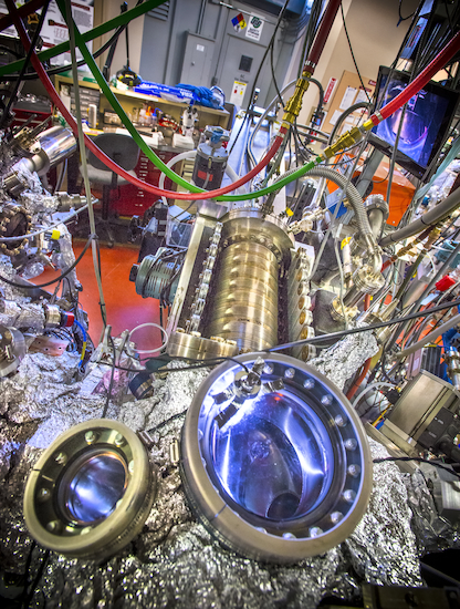
“Cool it!” That’s a prime directive for microprocessor chips and a promising new solution to meeting this imperative is in the offing. Researchers with the U.S. Department of Energy (DOE)’s Lawrence Berkeley National Laboratory (Berkeley Lab) have developed a “process friendly” technique that would enable the cooling of microprocessor chips through carbon nanotubes.

Frank Ogletree, a physicist with Berkeley Lab’s Materials Sciences Division, led a study in which organic molecules were used to form strong covalent bonds between carbon nanotubes and metal surfaces. This improved by six-fold the flow of heat from the metal to the carbon nanotubes, paving the way for faster, more efficient cooling of computer chips. The technique is done through gas vapor or liquid chemistry at low temperatures, making it suitable for the manufacturing of computer chips.

The Jan. 22, 2014 Berkeley Lab news release (also on EurekAlert), which originated the news item, describes the nature  of the problem in more detail,

Overheating is the bane of microprocessors. As transistors heat up, their performance can deteriorate to the point where they no longer function as transistors. With microprocessor chips becoming more densely packed and processing speeds continuing to increase, the overheating problem looms ever larger. The first challenge is to conduct heat out of the chip and onto the circuit board where fans and other techniques can be used for cooling. Carbon nanotubes have demonstrated exceptionally high thermal conductivity but their use for cooling microprocessor chips and other devices has been hampered by high thermal interface resistances in nanostructured systems.

“The thermal conductivity of carbon nanotubes exceeds that of diamond or any other natural material but because carbon nanotubes are so chemically stable, their chemical interactions with most other materials are relatively weak, which makes for  high thermal interface resistance,” Ogletree says. “Intel came to the Molecular Foundry wanting to improve the performance of carbon nanotubes in devices. Working with Nachiket Raravikar and Ravi Prasher, who were both Intel engineers when the project was initiated, we were able to increase and strengthen the contact between carbon nanotubes and the surfaces of other materials. This reduces thermal resistance and substantially improves heat transport efficiency.”

The news release then describes the proposed solution,

Sumanjeet Kaur, lead author of the Nature Communications paper and an expert on carbon nanotubes, with assistance from co-author and Molecular Foundry chemist Brett Helms, used reactive molecules to bridge the carbon nanotube/metal interface – aminopropyl-trialkoxy-silane (APS) for oxide-forming metals, and cysteamine for noble metals. First vertically aligned carbon nanotube arrays were grown on silicon wafers, and thin films of aluminum or gold were evaporated on glass microscope cover slips. The metal films were then “functionalized” and allowed to bond with the carbon nanotube arrays. Enhanced heat flow was confirmed using a characterization technique developed by Ogletree that allows for interface-specific measurements of heat transport.

“You can think of interface resistance in steady-state heat flow as being an extra amount of distance the heat has to flow through the material,” Kaur says. “With carbon nanotubes, thermal interface resistance adds something like 40 microns of distance on each side of the actual carbon nanotube layer. With our technique, we’re able to decrease the interface resistance so that the extra distance is around seven microns at each interface.”

Although the approach used by Ogletree, Kaur and their colleagues substantially strengthened the contact between a metal and individual carbon nanotubes within an array, a majority of the nanotubes within the array may still fail to connect with the metal. The Berkeley team is now developing a way to improve the density of carbon nanotube/metal contacts. Their technique should also be applicable to single and multi-layer graphene devices, which face the same cooling issues.

For anyone who’s never heard of the Molecular Foundry before (from the news release),

The Molecular Foundry is one of five DOE [Department of Energy] Nanoscale Science Research Centers (NSRCs), national user facilities for interdisciplinary research at the nanoscale, supported by the DOE Office of Science. Together the NSRCs comprise a suite of complementary facilities that provide researchers with state-of-the-art capabilities to fabricate, process, characterize, and model nanoscale materials, and constitute the largest infrastructure investment of the National Nanotechnology Initiative. The NSRCs are located at DOE’s Argonne, Brookhaven, Lawrence Berkeley, Oak Ridge and Sandia and Los Alamos national laboratories.

My second item comes from the University of Buffalo (UB), located in the US. From a Jan. 21, 2014 University of Buffalo news release by Cory Nealon (also on EurekAlert),

Heat in electronic devices is generated by the movement of electrons through transistors, resistors and other elements of an electrical network. Depending on the network, there are a variety of ways, such as cooling fans and heat sinks, to prevent the circuits from overheating.

But as more integrated circuits and transistors are added to devices to boost their computing power, it’s becoming more difficult to keep those elements cool. Most nanoelectrics research centers are working to develop advanced materials that are capable of withstanding the extreme environment inside smartphones, laptops and other devices.

While advanced materials show tremendous potential, the UB research suggests there may still be room within the existing paradigm of electronic devices to continue developing more powerful computers.

To support their findings, the researchers fabricated nanoscale semiconductor devices in a state-of-the-art gallium arsenide crystal provided to UB by Sandia’s Reno [John L. Reno, Center for Integrated Nanotechnologies at Sandia National Laboratories]. The researchers then subjected the chip to a large voltage, squeezing an electrical current through the nanoconductors. This, in turn, increased the amount of heat circulating through the chip’s nanotransistor.

But instead of degrading the device, the nanotransistor spontaneously transformed itself into a quantum state that was protected from the effect of heating and provided a robust channel of electric current. To help explain, Bird [Jonathan Bird, UB professor of electrical engineering] offered an analogy to Niagara Falls.

“The water, or energy, comes from a source; in this case, the Great Lakes. It’s channeled into a narrow point (the Niagara River) and ultimately flows over Niagara Falls. At the bottom of waterfall is dissipated energy. But unlike the waterfall, this dissipated energy recirculates throughout the chip and changes how heat affects, or in this case doesn’t affect, the network’s operation.”

While this behavior may seem unusual, especially conceptualizing it in terms of water flowing over a waterfall, it is the direct result of the quantum mechanical nature of electronics when viewed on the nanoscale. The current is made up of electrons which spontaneously organize to form a narrow conducting filament through the nanoconductor. It is this filament that is so robust against the effects of heating.

“We’re not actually eliminating the heat, but we’ve managed to stop it from affecting the electrical network. In a way, this is an optimization of the current paradigm,” said Han [J. E. Han, UB Dept. of Physics], who developed the theoretical models which explain the findings.

What an interesting and counter-intuitive approach to managing the heat in our devices.

For those who want more, here’s a link to and citation for the carbon nanotube paper,

Enhanced thermal transport at covalently functionalized carbon nanotube array interfaces by Sumanjeet Kaur, Nachiket Raravikar, Brett A. Helms, Ravi Prasher, & D. Frank Ogletree. Nature Communications 5, Article number: 3082 doi:10.1038/ncomms4082 Published 22 January 2014

This paper is behind a paywall.

Now here’s a link to and a citation for the ‘making it hotter to make it cooler’ paper,

Formation of a protected sub-band for conduction in quantum point contacts under extreme biasing by J. Lee, J. E. Han, S. Xiao, J. Song, J. L. Reno, & J. P. Bird. Nature Nanotechnology (2014) doi:10.1038/nnano.2013.297 Published online 19 January 2014

This paper is behind a paywall although there is an option to preview it for free via ReadCube Access.

Get yourself some e-whiskers for improved tactile sensing

E-whiskers are highly responsive tactile sensor networks made from carbon nanotubes and silver nanoparticles that resemble the whiskers of cats and other mammals. Courtesy: Berkeley Labs [downloaded from http://newscenter.lbl.gov/science-shorts/2014/01/20/e-whiskers/]

E-whiskers are highly responsive tactile sensor networks made from carbon nanotubes and silver nanoparticles that resemble the whiskers of cats and other mammals. Courtesy: Berkeley Labs [downloaded from http://newscenter.lbl.gov/science-shorts/2014/01/20/e-whiskers/]

A Jan. 21, 2014 news item on Azonano features work from researchers who have simulated the sensitivity of cat’s and rat’s whiskers by creating e-whiskers,

Researchers with Berkeley Lab and the University of California (UC) Berkeley have created tactile sensors from composite films of carbon nanotubes and silver nanoparticles similar to the highly sensitive whiskers of cats and rats. These new e-whiskers respond to pressure as slight as a single Pascal, about the pressure exerted on a table surface by a dollar bill. Among their many potential applications is giving robots new abilities to “see” and “feel” their surrounding environment.

The Jan. 20, 2014 Lawrence Berkeley National Laboratory (Berkeley Lab) ‘science short’ by Lynn Yarris, which originated the news item,  provides more information about the research,

“Whiskers are hair-like tactile sensors used by certain mammals and insects to monitor wind and navigate around obstacles in tight spaces,” says the leader of this research Ali Javey, a faculty scientist in Berkeley Lab’s Materials Sciences Division and a UC Berkeley professor of electrical engineering and computer science.  “Our electronic whiskers consist of high-aspect-ratio elastic fibers coated with conductive composite films of nanotubes and nanoparticles. In tests, these whiskers were 10 times more sensitive to pressure than all previously reported capacitive or resistive pressure sensors.”

Javey and his research group have been leaders in the development of e-skin and other flexible electronic devices that can interface with the environment. In this latest effort, they used a carbon nanotube paste to form an electrically conductive network matrix with excellent bendability. To this carbon nanotube matrix they loaded a thin film of silver nanoparticles that endowed the matrix with high sensitivity to mechanical strain.

“The strain sensitivity and electrical resistivity of our composite film is readily tuned by changing the composition ratio of the carbon nanotubes and the silver nanoparticles,” Javey says. “The composite can then be painted or printed onto high-aspect-ratio elastic fibers to form e-whiskers that can be integrated with different user-interactive systems.”

Javey notes that the use of elastic fibers with a small spring constant as the structural component of the whiskers provides large deflection and therefore high strain in response to the smallest applied pressures. As proof-of-concept, he and his research group successfully used their e-whiskers to demonstrate highly accurate 2D and 3D mapping of wind flow. In the future, e-whiskers could be used to mediate tactile sensing for the spatial mapping of nearby objects, and could also lead to wearable sensors for measuring heartbeat and pulse rate.

“Our e-whiskers represent a new type of highly responsive tactile sensor networks for real time monitoring of environmental effects,” Javey says. “The ease of fabrication, light weight and excellent performance of our e-whiskers should have a wide range of applications for advanced robotics, human-machine user interfaces, and biological applications.”

The researchers’ paper has been published in the Proceedings of the National Academy of Sciences and is titled: “Highly sensitive electronic whiskers based on patterned carbon nanotube and silver nanoparticle composite films.”

Here’s what the e-whiskers look like,

An array of seven vertically placed e-whiskers was used for 3D mapping of the wind by Ali Javey and his group [ Kuniharu Takei, Zhibin Yu, Maxwell Zheng, Hiroki Ota and Toshitake Takahashi].  Courtesy: Berkeley Lab

An array of seven vertically placed e-whiskers was used for 3D mapping of the wind by Ali Javey and his group [ Kuniharu Takei, Zhibin Yu, Maxwell Zheng, Hiroki Ota and Toshitake Takahashi]. Courtesy: Berkeley Lab

Finding a successor to graphene

The folks at the Lawrence Berkeley National Laboratory (Berkeley Lab) have announced a ‘natural’ 3D counterpart of graphene in a Jan. 16, 2014 Berkeley Lab news release (also on EurekAlert and on Azonano dated Jan. 17, 2014),

The discovery of what is essentially a 3D version of graphene – the 2D sheets of carbon through which electrons race at many times the speed at which they move through silicon – promises exciting new things to come for the high-tech industry, including much faster transistors and far more compact hard drives. A collaboration of researchers at the U.S Department of Energy (DOE)’s Lawrence Berkeley National Laboratory (Berkeley Lab) has discovered that sodium bismuthate can exist as a form of quantum matter called a three-dimensional topological Dirac semi-metal (3DTDS). This is the first experimental confirmation of 3D Dirac fermions in the interior or bulk of a material, a novel state that was only recently proposed by theorists.

The news release provides a description of graphene and the search for alternatives (counterparts),

Two of the most exciting new materials in the world of high technology today are graphene and topological insulators, crystalline materials that are electrically insulating in the bulk but conducting on the surface. Both feature 2D Dirac fermions (fermions that aren’t their own antiparticle), which give rise to extraordinary and highly coveted physical properties. Topological insulators also possess a unique electronic structure, in which bulk electrons behave like those in an insulator while surface electrons behave like those in graphene.

“The swift development of graphene and topological insulators has raised questions as to whether there are 3D counterparts and other materials with unusual topology in their electronic structure,” says Chen [Yulin Chen, a physicist from the University of Oxford who led this study working with Berkeley Lab’s Advanced Light Source (ALS)]. “Our discovery answers both questions. In the sodium bismuthate we studied, the bulk conduction and valence bands touch only at discrete points and disperse linearly along all three momentum directions to form bulk 3D Dirac fermions. Furthermore, the topology of a 3DTSD electronic structure is also as unique as those of topological insulators.”

I’m a bit puzzled as to how this new material can be described as “essentially a 3D version of graphene” as my understanding is that graphene must be composed of carbon and have a 2-dimensiional honeycomb structure to merit the name. In any event, this new material, sodium bismuthate, has some disadvantages but the discovery is an encouraging development (from the news release),

Sodium bismuthate is too unstable to be used in devices without proper packaging, but it triggers the exploration for the development of other 3DTDS materials more suitable for everyday devices, a search that is already underway. Sodium bismuthate can also be used to demonstrate potential applications of 3DTDS systems, which offer some distinct advantages over graphene.

“A 3DTDS system could provide a significant improvement in efficiency in many applications over graphene because of its 3D volume,” Chen says. “Also, preparing large-size atomically thin single domain graphene films is still a challenge. It could be easier to fabricate graphene-type devices for a wider range of applications from 3DTDS systems.”

In addition, Chen says, a 3DTDS system also opens the door to other novel physical properties, such as giant diamagnetism that diverges when energy approaches the 3D Dirac point, quantum magnetoresistance in the bulk, unique Landau level structures under strong magnetic fields, and oscillating quantum spin Hall effects. All of these novel properties can be a boon for future electronic technologies. Future 3DTDS systems can also serve as an ideal platform for applications in spintronics.

While I don’t understand (again) the image the researchers have included as an illustration of their work, I do find the ‘blue jewels in a pile of junk’ very appealing,

Beamline 10.0.1 at Berkeley Lab’s Advanced Light Source is optimized for the study of for electron structures and correlated electron systems. (Photo by Roy Kaltschmidt) Courtesy: Berkeley Lab

Beamline 10.0.1 at Berkeley Lab’s Advanced Light Source is optimized for the study of for electron structures and correlated electron systems. (Photo by Roy Kaltschmidt) Courtesy: Berkeley Lab

Here’s a link to and a citation for the paper,

Discovery of a Three-dimensional Topological Dirac Semimetal, Na3Bi by Zhongkai Liu, Bo Zhou, Yi Zhang, Zhijun Wang, Hongming Weng, Dharmalingam Prabhakaran, Sung-Kwan Mo, Zhi-Xun Shen, Zhong Fang, Xi Dai, and Zahid Hussain. Published Online January 16 2014 Science DOI: 10.1126/science.1245085

This paper is behind a paywall.

Graphene liquid cells and movies at the nanoscale

Here’s an Oct. 3, 2013 news item on Azonano about transmission electron microscopy (TEM) and graphene liquid cells enabling researchers at the Lawrence Berkeley National Laboratory (Berkeley Lab) to make movies,

Through a combination of transmission electron microscopy (TEM) and their own unique graphene liquid cell, the researchers have recorded the three-dimensional motion of DNA connected to gold nanocrystals. This is the first time TEM has been used for 3D dynamic imaging of so-called soft materials.

The researchers have produced an animation illustrating their work,

The Oct. 3, 2013 Berkeley Lab news release, which originated the news item, goes on to describe the challenge of imaging soft materials and how the researchers solved the problem,

In the past, liquid cells featured silicon-based viewing windows whose thickness limited resolution and perturbed the natural state of the soft materials. Zettl [physicist Alex Zettl] and Alivisatos [Paul Alivisatos, Berkeley Lab Director] and their respective research groups overcame these limitations with the development of a liquid cell based on a graphene membrane only a single atom thick. This development was done in close cooperation with researchers at the National Center for Electron Microscopy (NCEM), which is located at Berkeley Lab.

“Our graphene liquid cells pushed the spatial resolution of liquid phase TEM imaging to the atomic scale but still focused on growth trajectories of metallic nanocrystals,” says lead author Qian Chen, a postdoctoral fellow in Alivisatos’s research group. “Now we’ve adopted the technique to imaging the 3D dynamics of soft materials, starting with double-strand (dsDNA) connected to gold nanocrystals and achieved nanometer resolution.”

To create the cell, two opposing graphene sheets are bonded to one another by their van der Waals attraction. This forms a sealed nanoscale chamber and creates within the chamber a stable aqueous solution pocket approximately 100 nanometers in height and one micron in diameter. The single atom thick graphene membrane of the cells is essentially transparent to the TEM electron beam, minimizing the unwanted loss of imaging electrons and providing superior contrast and resolution compared to silicon-based windows. The aqueous pockets allow for up to two minutes of continuous imaging of soft material samples exposed to a 200 kilo Volt imaging electron beam. During this time, soft material samples can freely rotate.

After demonstrating that their graphene liquid cell can seal an aqueous sample solution against a TEM high vacuum, the Berkeley researchers used it to study the types of gold-dsDNA nanoconjugates that have been widely used as dynamic plasmonic probes.

“The presence of double-stranded DNA molecules incorporates the major challenges of studying the dynamics of biological samples with liquid phase TEM,” says Alivisatos. “The high-contrast gold nanocrystals facilitate tracking of our specimens.”

The Alivisatos and Zettl groups were able to observe dimers, pairs of gold nanoparticles, tethered by a single piece of dsDNA, and trimers, three gold nanoparticles, connected into a linear configuration by two single pieces of dsDNA. From a series of 2D projected TEM images captured while the samples were rotating, the researchers were to reconstruct 3D configuration and motions of the samples as they evolved over time.

Smarter ‘smart’ windows

It seems to me we may have to find a new way to discuss ‘smart’ windows as there’s only one more category after the comparative  ‘smarter’ and that’s the superlative ‘smartest’. Lawrence Berkeley National Laboratory (Berkeley Lab), please, let’s stop the madness now! That said, the Berkeley Lab issued an Aug. 14, 2013 news release  (also on EurekAlert) about it’s latest work on raising the IQ of smart windows,

Researchers at the U.S. Department of Energy’s Lawrence Berkeley National Laboratory (Berkeley Lab) have designed a new material to make smart windows even smarter. The material is a thin coating of nanocrystals embedded in glass that can dynamically modify sunlight as it passes through a window. Unlike existing technologies, the coating provides selective control over visible light and heat-producing near-infrared (NIR) light, so windows can maximize both energy savings and occupant comfort in a wide range of climates.

Milliron’s research group is already well known for their smart-window technology that blocks NIR without blocking visible light. The technology hinges on an electrochromic effect, where a small jolt of electricity switches the material between NIR-transmitting and NIR-blocking states. This new work takes their approach to the next level by providing independent control over both visible and NIR light. The innovation was recently recognized with a 2013 R&D 100 Award and the researchers are in the early stages of commercializing their technology.

Independent control over NIR light means that occupants can have natural lighting indoors without unwanted thermal gain, reducing the need for both air-conditioning and artificial lighting. The same window can also be switched to a dark mode, blocking both light and heat, or to a bright, fully transparent mode.

“We’re very excited about the combination of unique optical function with the low-cost and environmentally friendly processing technique,” said Llordés, a project scientist working with Milliron. “That’s what turns this ‘universal smart window’ concept into a promising competitive technology.”

Here’s the specific technology that’s been developed, from the news release,

At the heart of their technology is a new “designer” electrochromic material, made from nanocrystals of indium tin oxide embedded in a glassy matrix of niobium oxide. The resulting composite material combines two distinct functionalities—one providing control over visible light and the other, control over NIR—but it is more than the sum of its parts. The researchers found a synergistic interaction in the tiny region where glassy matrix meets nanocrystal that increases the potency of the electrochromic effect, which means they can use thinner coatings without compromising performance. The key is that the way atoms connect across the nanocrystal-glass interface causes a structural rearrangement in the glass matrix. The interaction opens up space inside the glass, allowing charge to move in and out more readily. Beyond electrochromic windows, this discovery suggests new opportunities for battery materials where transport of ions through electrodes can be a challenge.

I notice they’re using indium, one of the ‘rare earths’. Last I heard, China, one of the main sources for ‘rare earths’, was limiting its exports so this seems like an odd choice of material. Perhaps now they’ve proved this can be done,  they’ll research for easily available substitutes. Here’s a link to and a citation for the published paper,

Tunable near-infrared and visible-light transmittance in nanocrystal-in-glass composites by Anna Llordés, Guillermo Garcia, Jaume Gazquez, & Delia J. Milliron. Nature 500, 323–326 (15 August 2013) doi:10.1038/nature12398 Published online 14 August 2013

Finally, the researchers have provided an illustration of indium tin oxide nanocrystals,

Nanocrystals of indium tin oxide (shown here in blue) embedded in a glassy matrix of niobium oxide (green) form a composite material that can switch between NIR-transmitting and NIR-blocking states with a small jolt of electricity. A synergistic interaction in the region where glassy matrix meets nanocrystal increases the potency of the electrochromic effect. Courtesy Berkeley Lab

Nanocrystals of indium tin oxide (shown here in blue) embedded in a glassy matrix of niobium oxide (green) form a composite material that can switch between NIR-transmitting and NIR-blocking states with a small jolt of electricity. A synergistic interaction in the region where glassy matrix meets nanocrystal increases the potency of the electrochromic effect. Courtesy Berkeley Lab

Integrated artificial photosynthesis nanosystem, a first for Lawrence Berkeley National Laboratory

There’s such a thing as too much information and not enough knowledge, a condition I’m currently suffering from with regard to artificial photosynthesis. Before expanding on that theme, here’s the latest about artificial photosynthesis from a May 16, 2013 Lawrence Berkeley National Laboratory news release (also available on EurekAlert),

In the wake of the sobering news that atmospheric carbon dioxide is now at its highest level in at least three million years, an important advance in the race to develop carbon-neutral renewable energy sources has been achieved. Scientists with the U.S. Department of Energy (DOE)’s Lawrence Berkeley National Laboratory (Berkeley Lab) have reported the first fully integrated nanosystem for artificial photosynthesis. While “artificial leaf” is the popular term for such a system, the key to this success was an “artificial forest.”

Here’s a more detailed description of the system, from the news release,

“Similar to the chloroplasts in green plants that carry out photosynthesis, our artificial photosynthetic system is composed of two semiconductor light absorbers, an interfacial layer for charge transport, and spatially separated co-catalysts,” says Peidong Yang, a chemist with Berkeley Lab’s Materials Sciences Division, who led this research. “To facilitate solar water- splitting in our system, we synthesized tree-like nanowire  heterostructures, consisting of silicon trunks and titanium oxide branches. Visually, arrays of these nanostructures very much resemble an artificial forest.”

… Artificial photosynthesis, in which solar energy is directly converted into chemical fuels, is regarded as one of the most promising of solar technologies. A major challenge for artificial photosynthesis is to produce hydrogen cheaply enough to compete with fossil fuels. Meeting this challenge requires an integrated system that can efficiently absorb sunlight and produce charge-carriers to drive separate water reduction and oxidation half-reactions.

More specifically,

“In natural photosynthesis the energy of absorbed sunlight produces energized charge-carriers that execute chemical reactions in separate regions of the chloroplast,” Yang says. “We’ve integrated our nanowire nanoscale heterostructure into a functional system that mimics the integration in chloroplasts and provides a conceptual blueprint for better solar-to-fuel conversion efficiencies in the future.”

When sunlight is absorbed by pigment molecules in a chloroplast, an energized electron is generated that moves from molecule to molecule through a transport chain until ultimately it drives the conversion of carbon dioxide into carbohydrate sugars. This electron transport chain is called a “Z-scheme” because the pattern of movement resembles the letter Z on its side. Yang and his colleagues also use a Z-scheme in their system only they deploy two Earth abundant and stable semiconductors – silicon and titanium oxide – loaded with co-catalysts and with an ohmic contact inserted between them. Silicon was used for the hydrogen-generating photocathode and titanium oxide for the oxygen-generating photoanode. The tree-like architecture was used to maximize the system’s performance. Like trees in a real forest, the dense arrays of artificial nanowire trees suppress sunlight reflection and provide more surface area for fuel producing reactions.

“Upon illumination photo-excited electron−hole pairs are generated in silicon and titanium oxide, which absorb different regions of the solar spectrum,” Yang says. “The photo-generated electrons in the silicon nanowires migrate to the surface and reduce protons to generate hydrogen while the photo-generated holes in the titanium oxide nanowires oxidize water to evolve  oxygen molecules. The majority charge carriers from both semiconductors recombine at the ohmic contact, completing the relay of the Z-scheme, similar to that of natural photosynthesis.”

Under simulated sunlight, this integrated nanowire-based artificial photosynthesis system achieved a 0.12-percent solar-to-fuel conversion efficiency. Although comparable to some natural photosynthetic conversion efficiencies, this rate will have to be substantially improved for commercial use. [emphasis mine] However, the modular design of this system allows for newly discovered individual components to be readily incorporated to improve its performance. For example, Yang notes that the photocurrent output from the system’s silicon cathodes and titanium oxide anodes do not match, and that the lower photocurrent output from the anodes is limiting the system’s overall performance.

“We have some good ideas to develop stable photoanodes with better performance than titanium oxide,” Yang says. “We’re confident that we will be able to replace titanium oxide anodes in the near future and push the energy conversion efficiency up into single digit percentages.”

Now I can discuss my confusion, which stems from my May 24, 2013 posting about work done at the Argonne National Laboratory,

… Researchers still have a long way to go before they will be able to create devices that match the light harvesting efficiency of a plant.

One reason for this shortcoming, Tiede [Argonne biochemist David Tiede] explained, is that artificial photosynthesis experiments have not been able to replicate the molecular matrix that contains the chromophores. “The level that we are at with artificial photosynthesis is that we can make the pigments and stick them together, but we cannot duplicate any of the external environment,” he said.  “The next step is to build in this framework, and then these kinds of quantum effects may become more apparent.”

Because the moment when the quantum effect occurs is so short-lived – less than a trillionth of a second – scientists will have a hard time ascertaining biological and physical rationales for their existence in the first place. [emphasis mine]

It’s not clear to me whether or not the folks at the Berkeley Lab bypassed the ‘problem’ described by Tiede or solved it to achieve solar-to-fuel conversion rates comparable to natural photosynthesis conversions. As I noted, too much information/not enough knowledge.