Tag Archives: Brian D. Hoskins

Thanks for the memory: the US National Institute of Standards and Technology (NIST) and memristors

In January 2018 it seemed like I was tripping across a lot of memristor stories . This came from a January 19, 2018 news item on Nanowerk,

In the race to build a computer that mimics the massive computational power of the human brain, researchers are increasingly turning to memristors, which can vary their electrical resistance based on the memory of past activity. Scientists at the National Institute of Standards and Technology (NIST) have now unveiled the long-mysterious inner workings of these semiconductor elements, which can act like the short-term memory of nerve cells.

A January 18, 2018 NIST news release (also on EurekAlert), which originated the news item, fills in the details,

Just as the ability of one nerve cell to signal another depends on how often the cells have communicated in the recent past, the resistance of a memristor depends on the amount of current that recently flowed through it. Moreover, a memristor retains that memory even when electrical power is switched off.

But despite the keen interest in memristors, scientists have lacked a detailed understanding of how these devices work and have yet to develop a standard toolset to study them.

Now, NIST scientists have identified such a toolset and used it to more deeply probe how memristors operate. Their findings could lead to more efficient operation of the devices and suggest ways to minimize the leakage of current.

Brian Hoskins of NIST and the University of California, Santa Barbara, along with NIST scientists Nikolai Zhitenev, Andrei Kolmakov, Jabez McClelland and their colleagues from the University of Maryland’s NanoCenter (link is external) in College Park and the Institute for Research and Development in Microtechnologies in Bucharest, reported the findings (link is external) in a recent Nature Communications.

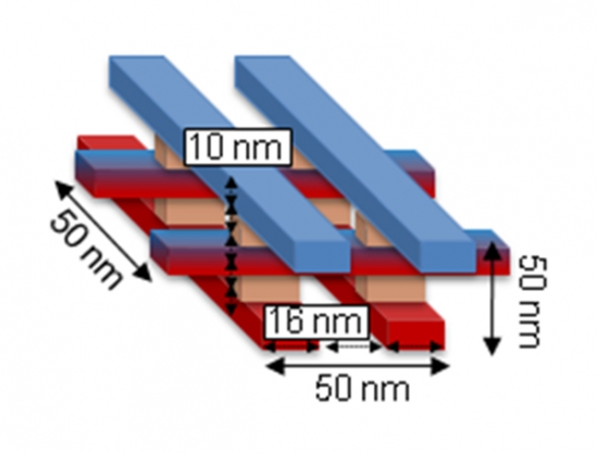
To explore the electrical function of memristors, the team aimed a tightly focused beam of electrons at different locations on a titanium dioxide memristor. The beam knocked free some of the device’s electrons, which formed ultrasharp images of those locations. The beam also induced four distinct currents to flow within the device. The team determined that the currents are associated with the multiple interfaces between materials in the memristor, which consists of two metal (conducting) layers separated by an insulator.

“We know exactly where each of the currents are coming from because we are controlling the location of the beam that is inducing those currents,” said Hoskins.

In imaging the device, the team found several dark spots—regions of enhanced conductivity—which indicated places where current might leak out of the memristor during its normal operation. These leakage pathways resided outside the memristor’s core—where it switches between the low and high resistance levels that are useful in an electronic device. The finding suggests that reducing the size of a memristor could minimize or even eliminate some of the unwanted current pathways. Although researchers had suspected that might be the case, they had lacked experimental guidance about just how much to reduce the size of the device.

Because the leakage pathways are tiny, involving distances of only 100 to 300 nanometers, “you’re probably not going to start seeing some really big improvements until you reduce dimensions of the memristor on that scale,” Hoskins said.

To their surprise, the team also found that the current that correlated with the memristor’s switch in resistance didn’t come from the active switching material at all, but the metal layer above it. The most important lesson of the memristor study, Hoskins noted, “is that you can’t just worry about the resistive switch, the switching spot itself, you have to worry about everything around it.” The team’s study, he added, “is a way of generating much stronger intuition about what might be a good way to engineer memristors.”

Here’s a link to and a citation for the paper,

Stateful characterization of resistive switching TiO2 with electron beam induced currents by Brian D. Hoskins, Gina C. Adam, Evgheni Strelcov, Nikolai Zhitenev, Andrei Kolmakov, Dmitri B. Strukov, & Jabez J. McClelland. Nature Communications 8, Article number: 1972 (2017) doi:10.1038/s41467-017-02116-9 Published online: 07 December 2017

This is an open access paper.

It might be my imagination but it seemed like a lot of papers from 2017 were being publicized in early 2018.

Finally, I borrowed much of my headline from the NIST’s headline for its news release, specifically, “Thanks for the memory,” which is a rather old song,

Bob Hope and Shirley Ross in “The Big Broadcast of 1938.”

The memristor as computing device

An Oct. 27, 2016 news item on Nanowerk both builds on the Richard Feynman legend/myth and announces some new work with memristors,

In 1959 renowned physicist Richard Feynman, in his talk “[There’s] Plenty of Room at the Bottom,” spoke of a future in which tiny machines could perform huge feats. Like many forward-looking concepts, his molecule and atom-sized world remained for years in the realm of science fiction.

And then, scientists and other creative thinkers began to realize Feynman’s nanotechnological visions.

In the spirit of Feynman’s insight, and in response to the challenges he issued as a way to inspire scientific and engineering creativity, electrical and computer engineers at UC Santa Barbara [University of California at Santa Barbara, UCSB] have developed a design for a functional nanoscale computing device. The concept involves a dense, three-dimensional circuit operating on an unconventional type of logic that could, theoretically, be packed into a block no bigger than 50 nanometers on any side.

A figure depicting the structure of stacked memristors with dimensions that could satisfy the Feynman Grand Challenge Photo Credit: Courtesy Image

A figure depicting the structure of stacked memristors with dimensions that could satisfy the Feynman Grand Challenge. Photo Credit: Courtesy Image

An Oct. 27, 2016 UCSB news release (also on EurekAlert) by Sonia Fernandez, which originated the news item, offers a basic explanation of the work (useful for anyone unfamiliar with memristors) along with more detail,

“Novel computing paradigms are needed to keep up with the demand for faster, smaller and more energy-efficient devices,” said Gina Adam, postdoctoral researcher at UCSB’s Department of Computer Science and lead author of the paper “Optimized stateful material implication logic for three dimensional data manipulation,” published in the journal Nano Research. “In a regular computer, data processing and memory storage are separated, which slows down computation. Processing data directly inside a three-dimensional memory structure would allow more data to be stored and processed much faster.”

While efforts to shrink computing devices have been ongoing for decades — in fact, Feynman’s challenges as he presented them in his 1959 talk have been met — scientists and engineers continue to carve out room at the bottom for even more advanced nanotechnology. A nanoscale 8-bit adder operating in 50-by-50-by-50 nanometer dimension, put forth as part of the current Feynman Grand Prize challenge by the Foresight Institute, has not yet been achieved. However, the continuing development and fabrication of progressively smaller components is bringing this virus-sized computing device closer to reality, said Dmitri Strukov, a UCSB professor of computer science.

“Our contribution is that we improved the specific features of that logic and designed it so it could be built in three dimensions,” he said.

Key to this development is the use of a logic system called material implication logic combined with memristors — circuit elements whose resistance depends on the most recent charges and the directions of those currents that have flowed through them. Unlike the conventional computing logic and circuitry found in our present computers and other devices, in this form of computing, logic operation and information storage happen simultaneously and locally. This greatly reduces the need for components and space typically used to perform logic operations and to move data back and forth between operation and memory storage. The result of the computation is immediately stored in a memory element, which prevents data loss in the event of power outages — a critical function in autonomous systems such as robotics.

In addition, the researchers reconfigured the traditionally two-dimensional architecture of the memristor into a three-dimensional block, which could then be stacked and packed into the space required to meet the Feynman Grand Prize Challenge.

“Previous groups show that individual blocks can be scaled to very small dimensions, let’s say 10-by-10 nanometers,” said Strukov, who worked at technology company Hewlett-Packard’s labs when they ramped up development of memristors and material implication logic. By applying those results to his group’s developments, he said, the challenge could easily be met.

The tiny memristors are being heavily researched in academia and in industry for their promising uses in memory storage and neuromorphic computing. While implementations of material implication logic are rather exotic and not yet mainstream, uses for it could pop up any time, particularly in energy scarce systems such as robotics and medical implants.

“Since this technology is still new, more research is needed to increase its reliability and lifetime and to demonstrate large scale three-dimensional circuits tightly packed in tens or hundreds of layers,” Adam said.

HP Labs, mentioned in the news release, announced the ‘discovery’ of memristors and subsequent application of engineering control in two papers in 2008.

Here’s a link to and a citation for the UCSB paper,

Optimized stateful material implication logic for threedimensional data manipulation by Gina C. Adam, Brian D. Hoskins, Mirko Prezioso, &Dmitri B. Strukov. Nano Res. (2016) pp. 1 – 10. doi:10.1007/s12274-016-1260-1 First Online: 29 September 2016

This paper is behind a paywall.

You can find many articles about memristors here by using either ‘memristor’ or ‘memristors’ as your search term.