Tag Archives: Caltech

Make electricity by flowing water over nanolayers of metal

Scientists at Northwestern University (Chicago, Illinois) and the California Institute of Technology (CalTech) have developed what could be a more sustainable way to produce electricity. From a July 31, 2019 news item on Nanowerk,

Scientists from Northwestern University and Caltech have produced electricity by simply flowing water over extremely thin layers of inexpensive metals, including iron, that have oxidized. These films represent an entirely new way of generating electricity and could be used to develop new forms of sustainable power production.

A July 31, 2019 Northwester University news release (also on EurekAlert) by Megan Fellman, which originated the news item, provides details that suggest this discovery could prove beneficial in medical implants, as well as, in solar cells,

The films have a conducting metal nanolayer (10 to 20 nanometers thick) that is insulated with an oxide layer (2 nanometers thick). Current is generated when pulses of rainwater and ocean water alternate and move across the nanolayers. The difference in salinity drags the electrons along in the metal below.

“It’s the oxide layer over the nanometal that really makes this device go,” said Franz M. Geiger, the Dow Professor of Chemistry in Northwestern’s Weinberg College of Arts and Sciences. “Instead of corrosion, the presence of the oxides on the right metals leads to a mechanism that shuttles electrons.”

The films are transparent, a feature that could be taken advantage of in solar cells. The researchers intend to study the method using other ionic liquids, including blood. Developments in this area could lead to use in stents and other implantable devices.

“The ease of scaling up the metal nanolayer to large areas and the ease with which plastics can be coated gets us to three-dimensional structures where large volumes of liquids can be used,” Geiger said. “Foldable designs that fit, for instance, into a backpack are a possibility as well. Given how transparent the films are, it’s exciting to think about coupling the metal nanolayers to a solar cell or coating the outside of building windows with metal nanolayers to obtain energy when it rains.”

The study, titled “Energy Conversion via Metal Nanolayers,” was published this week [on July 29, 2019] in the journal Proceedings of the National Academy of Sciences (PNAS).

Geiger is the study’s corresponding author; his Northwestern team conducted the experiments. Co-author Thomas Miller, professor of chemistry at Caltech, led a team that conducted atomistic simulations to study the device’s behavior at the atomic level.

The new method produces voltages and currents comparable to graphene-based devices reported to have efficiencies of around 30% — similar to other approaches under investigation (carbon nanotubes and graphene) but with a single-step fabrication from earth-abundant elements instead of multistep fabrication. This simplicity allows for scalability, rapid implementation and low cost. Northwestern has filed for a provisional patent.

Of the metals studied, the researchers found that iron, nickel and vanadium worked best. They tested a pure rust sample as a control experiment; it did not produce a current.

The mechanism behind the electricity generation is complex, involving ion adsorption and desorption, but it essentially works like this: The ions present in the rainwater/saltwater attract electrons in the metal beneath the oxide layer; as the water flows, so do those ions, and through that attractive force, they drag the electrons in the metal along with them, generating an electrical current.

“There are interesting prospects for a variety of energy and sustainability applications, but the real value is the new mechanism of oxide-metal electron transfer,” Geiger said. “The underlying mechanism appears to involve various oxidation states.”

The team used a process called physical vapor deposition (PVD), which turns normally solid materials into a vapor that condenses on a desired surface. PVD allowed them to deposit onto glass metal layers only 10 to 20 nanometers thick. An oxide layer then forms spontaneously in air. It grows to a thickness of 2 nanometers and then stops growing.

“Thicker films of metal don’t succeed — it’s a nano-confinement effect,” Geiger said. “We have discovered the sweet spot.”

When tested, the devices generated several tens of millivolts and several microamps per centimeter squared.

“For perspective, plates having an area of 10 square meters each would generate a few kilowatts per hour — enough for a standard U.S. home,” Miller said. “Of course, less demanding applications, including low-power devices in remote locations, are more promising in the near term.”

Here’s a link to and a citation for the paper,

Energy conversion via metal nanolayers by Mavis D. Boamah, Emilie H. Lozier, Jeongmin Kim, Paul E. Ohno, Catherine E. Walker, Thomas F. Miller III, and Franz M. Geiger. PNAS DOI: https://doi.org/10.1073/pnas.1906601116 First published July 29, 2019

This paper is behind a paywall.
Sticky at any temperature and other American Chemical Society News

Just when I thought I’d seen all the carbon nanotube abbreviations; I find two new ones in my first news bit about adhesion. Later, I’m including a second news bit that has to do with the upcoming American Chemical Society (ACS) Meeting in San Diego, California.

Sticky carbon nanotubes (CNTs)

Scientists have developed an adhesive that retains its stickiness in extreme temperatures according to a July 10, 2019 news item on Nanowerk (Note: A link has been removed),

In very hot or cold environments, conventional tape can lose its stickiness and leave behind an annoying residue. But while most people can avoid keeping taped items in a hot car or freezer, those living in extreme environments such as deserts and the Antarctic often can’t avoid such conditions.

Now, researchers reporting in ACS’ journal Nano Letters (“Continuous, Ultra-lightweight, and Multipurpose Super-aligned Carbon Nanotube Tapes Viable over a Wide Range of Temperatures”) say they have developed a new nanomaterial tape that can function over a wide temperature range.

In previous work, researchers have explored using nanomaterials, such as vertically aligned multi-walled carbon nanotubes (VA-MWNTs), to make better adhesive tapes. Although VA-MWNTs are stronger than conventional tapes at both high and low temperatures, the materials are relatively thick, and large amounts can’t be made cost-effectively.

These are my first vertically aligned multi-walled carbon nanotubes (VA-MWNTs) and superaligned carbon nanotubes (SACNTs). I was a little surprised that VA-MWNTs didn’t include the C since these are carbon nanotubes (CNTs) and there are other types of nanotubes. So, I searched and found that inclusion of the letter ‘C’ for carbon seems to be discretionary. Moving on.

A July 10, 2019 ACS press release (also on EurekAlert), which originated the news item, provides more detail,

… Kai Liu, Xide Li, Wenhui Duan, Kaili Jiang and coworkers wondered if they could develop a new type of tape composed of superaligned carbon nanotube (SACNT) films. As their name suggests, SACNTs are nanotubes that are precisely aligned parallel to each other, capable of forming ultrathin but strong yarns or films.

To make their tape, the researchers pulled a film from the interior of an array of SACNTs — similar to pulling a strip of tape from a roll. The resulting double-sided tape could adhere to surfaces through van der Waals interactions, which are weak electric forces generated between two atoms or molecules that are close together. The ultrathin, ultra-lightweight and flexible tape outperformed conventional adhesives, at temperatures ranging from -321 F to 1,832 F. Researchers could remove the tape by peeling it off, soaking it in acetone or burning it, with no noticeable residues. The tape adhered to many different materials such as metals, nonmetals, plastics and ceramics, but it stuck more strongly to smooth than rough surfaces, similar to regular tape. The SACNT tape can be made cost-effectively in large amounts. In addition to performing well in extreme environments, the new tape might be useful for electronic components that heat up during use, the researchers say.

Here’s a link to and a citation for the paper,

Continuous, Ultra-lightweight, and Multipurpose Super-aligned Carbon Nanotube Tapes Viable over a Wide Range of Temperatures by Xiang Jin, Hengxin Tan, Zipeng Wu, Jiecun Liang, Wentao Miao, Chao-Sheng Lian, Jiangtao Wang, Kai Liu, Haoming Wei, Chen Feng, Peng Liu, Yang Wei, Qunqing Li, Jiaping Wang, Liang Liu, Xide Li, Shoushan Fan, Wenhui Duan, Kaili Jiang. Nano Lett.2019 DOI: https://doi.org/10.1021/acs.nanolett.9b01629 Publication Date:June 16, 2019 Copyright © 2019 American Chemical Society

This paper is behind a paywall.

American Chemical Society (ACS) National Meeting in San Diego, Aug. 25 to 29, 2019: an invite to journalists

A July 18, 2019 ACS press release (received via email) announced their upcoming meeting and it included an invitation to journalists. (ACS has two meetings per year, one on the East Coast and the other on the West, roughly speaking).

Materials science and nanotechnology topics at the upcoming 2019 American Chemical Society national meeting in San Diego

WASHINGTON, July 18, 2019 — Journalists who register for the American Chemical Society’s (ACS’) Fall 2019 National Meeting & Exposition in San Diego will have access to more than 9,500 presentations on the meeting’s theme, “Chemistry & Water,” will include  nanotechnology and materials science topics. The meeting, one of the largest scientific conferences of the year, will be held Aug. 25 to 29 [2019] in San Diego.

Nobel Prize winner Frances Arnold, Ph.D., of the California Institute of Technology and Thomas Markland, DPhil, of Stanford University will deliver the two Kavli Foundation lectures on Aug. 26 [2019].

The more than 9,500 presentations will include presentations on nanotechnology and materials science, such as: 

Colloids and nanomaterials for water purification
Nanozymes for bioanalysis and beyond
The latest in wearable and implantable sensors
Nanoscale and molecular assemblies: designing matter to control energy transport
Colloidal quantum dots for solar and other emerging technologies
Nanoscience of bourbon
Targeted delivery of nanomedicines 
Advances in nanocellulose research for engineered functionality
Water sustainability through nanotechnology

Looking for something else? Search the meeting’s abstracts

ACS will operate a press center with press conferences, a news media workroom fully staffed to assist in arranging interviews and free Wi-Fi, computers and refreshments.

Embargoed copies of press releases and a press conference schedule will be available in mid-August.  Reporters planning to cover the meeting from their home bases will have access to the press conferences on YouTube at http://bit.ly/acs2019sandiego.

ACS considers requests for press credentials and complimentary registration to national meetings from reporters (staff and freelance) and public information officers at government, non-profit and educational institutions. See the website for details.

Here’s who does and doesn’t quality for a free press registration (from the ACS complimentary registration webpage),

Press Registration Requirements

The ACS provides complimentary registration to national meetings to reporters (staff and freelancers) and public information officers from government, non-profit and educational institutions. Marketing and public relations professionals, lobbyists and scientists do not qualify as press and must register via the main meeting registration page. Journal managing editors, book commissioning editors, acquisitions editors, publishers and those who do not produce news for a publication or institution also do not qualify. We reserve the right to refuse press credentials for any reason.

No bloggers, eh? it’s been a long time since I’ve seen a press registration process that doesn’t mention bloggers at all.

Spooling strips of graphene

An April 18, 2018 news item on phys.org highlights an exciting graphene development at the Massachusetts Institute of Technology (MIT),

MIT engineers have developed a continuous manufacturing process that produces long strips of high-quality graphene.

The team’s results are the first demonstration of an industrial, scalable method for manufacturing high-quality graphene that is tailored for use in membranes that filter a variety of molecules, including salts, larger ions, proteins, or nanoparticles. Such membranes should be useful for desalination, biological separation, and other applications.

A new manufacturing process produces strips of graphene, at large scale, for use in membrane technologies and other applications. Image: Christine Daniloff, MIT

An April 17, 2018 MIT news release (also on EurekAlert) by Jennifer Chu, which originated the news item,. provides more detail,

“For several years, researchers have thought of graphene as a potential route to ultrathin membranes,” says John Hart, associate professor of mechanical engineering and director of the Laboratory for Manufacturing and Productivity at MIT. “We believe this is the first study that has tailored the manufacturing of graphene toward membrane applications, which require the graphene to be seamless, cover the substrate fully, and be of high quality.”

Hart is the senior author on the paper, which appears online in the journal Applied Materials and Interfaces. The study includes first author Piran Kidambi, a former MIT postdoc who is now an assistant professor at Vanderbilt University; MIT graduate students Dhanushkodi Mariappan and Nicholas Dee; Sui Zhang of the National University of Singapore; Andrey Vyatskikh, a former student at the Skolkovo Institute of Science and Technology who is now at Caltech; and Rohit Karnik, an associate professor of mechanical engineering at MIT.

Growing graphene

For many researchers, graphene is ideal for use in filtration membranes. A single sheet of graphene resembles atomically thin chicken wire and is composed of carbon atoms joined in a pattern that makes the material extremely tough and impervious to even the smallest atom, helium.

Researchers, including Karnik’s group, have developed techniques to fabricate graphene membranes and precisely riddle them with tiny holes, or nanopores, the size of which can be tailored to filter out specific molecules. For the most part, scientists synthesize graphene through a process called chemical vapor deposition, in which they first heat a sample of copper foil and then deposit onto it a combination of carbon and other gases.

Graphene-based membranes have mostly been made in small batches in the laboratory, where researchers can carefully control the material’s growth conditions. However, Hart and his colleagues believe that if graphene membranes are ever to be used commercially they will have to be produced in large quantities, at high rates, and with reliable performance.

“We know that for industrialization, it would need to be a continuous process,” Hart says. “You would never be able to make enough by making just pieces. And membranes that are used commercially need to be fairly big – some so big that you would have to send a poster-wide sheet of foil into a furnace to make a membrane.”

A factory roll-out

The researchers set out to build an end-to-end, start-to-finish manufacturing process to make membrane-quality graphene.

The team’s setup combines a roll-to-roll approach – a common industrial approach for continuous processing of thin foils – with the common graphene-fabrication technique of chemical vapor deposition, to manufacture high-quality graphene in large quantities and at a high rate. The system consists of two spools, connected by a conveyor belt that runs through a small furnace. The first spool unfurls a long strip of copper foil, less than 1 centimeter wide. When it enters the furnace, the foil is fed through first one tube and then another, in a “split-zone” design.

While the foil rolls through the first tube, it heats up to a certain ideal temperature, at which point it is ready to roll through the second tube, where the scientists pump in a specified ratio of methane and hydrogen gas, which are deposited onto the heated foil to produce graphene.

“Graphene starts forming in little islands, and then those islands grow together to form a continuous sheet,” Hart says. “By the time it’s out of the oven, the graphene should be fully covering the foil in one layer, kind of like a continuous bed of pizza.”

As the graphene exits the furnace, it’s rolled onto the second spool. The researchers found that they were able to feed the foil continuously through the system, producing high-quality graphene at a rate of 5 centimers per minute. Their longest run lasted almost four hours, during which they produced about 10 meters of continuous graphene.

“If this were in a factory, it would be running 24-7,” Hart says. “You would have big spools of foil feeding through, like a printing press.”

Flexible design

Once the researchers produced graphene using their roll-to-roll method, they unwound the foil from the second spool and cut small samples out. They cast the samples with a polymer mesh, or support, using a method developed by scientists at Harvard University, and subsequently etched away the underlying copper.

“If you don’t support graphene adequately, it will just curl up on itself,” Kidambi says. “So you etch copper out from underneath and have graphene directly supported by a porous polymer – which is basically a membrane.”

The polymer covering contains holes that are larger than graphene’s pores, which Hart says act as microscopic “drumheads,” keeping the graphene sturdy and its tiny pores open.

The researchers performed diffusion tests with the graphene membranes, flowing a solution of water, salts, and other molecules across each membrane. They found that overall, the membranes were able to withstand the flow while filtering out molecules. Their performance was comparable to graphene membranes made using conventional, small-batch approaches.

The team also ran the process at different speeds, with different ratios of methane and hydrogen gas, and characterized the quality of the resulting graphene after each run. They drew up plots to show the relationship between graphene’s quality and the speed and gas ratios of the manufacturing process. Kidambi says that if other designers can build similar setups, they can use the team’s plots to identify the settings they would need to produce a certain quality of graphene.

“The system gives you a great degree of flexibility in terms of what you’d like to tune graphene for, all the way from electronic to membrane applications,” Kidambi says.

Looking forward, Hart says he would like to find ways to include polymer casting and other steps that currently are performed by hand, in the roll-to-roll system.

“In the end-to-end process, we would need to integrate more operations into the manufacturing line,” Hart says. “For now, we’ve demonstrated that this process can be scaled up, and we hope this increases confidence and interest in graphene-based membrane technologies, and provides a pathway to commercialization.”

Here’s a link to and a citation for the paper,

A Scalable Route to Nanoporous Large-Area Atomically Thin Graphene Membranes by Roll-to-Roll Chemical Vapor Deposition and Polymer Support Casting by Piran R. Kidambi, Dhanushkodi D. Mariappan, Nicholas T. Dee, Andrey Vyatskikh, Sui Zhang, Rohit Karnik, and A. John Hart. ACS Appl. Mater. Interfaces, 2018, 10 (12), pp 10369–10378 DOI: 10.1021/acsami.8b00846 Publication Date (Web): March 19, 2018

Copyright © 2018 American Chemical Society

This paper is behind a paywall.

Finally, there is a video of the ‘graphene spooling out’ process,

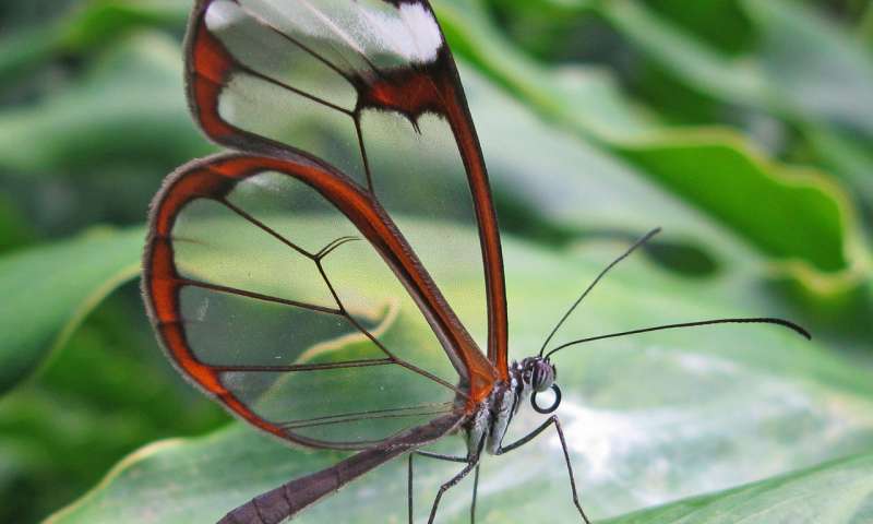
Eye implants inspired by glasswing butterflies

Glasswinged butterfly. Greta oto. Credit: David Tiller/CC BY-SA 3.0

My jaw dropped on seeing this image and I still have trouble believing it’s real. (You can find more image of glasswinged butterflies here in an Cot. 25, 2014 posting on thearkinspace. com and there’s a video further down in the post.)

As for the research, an April 30, 2018 news item on phys.org announces work that could improve eye implants,

Inspired by tiny nanostructures on transparent butterfly wings, engineers at Caltech have developed a synthetic analogue for eye implants that makes them more effective and longer-lasting. A paper about the research was published in Nature Nanotechnology.

An April 30, 2018 California Institute of Technology (CalTech) news release (also on EurekAlert) by Robert Perkins, which originated the news item, goes into more detail,

Sections of the wings of a longtail glasswing butterfly are almost perfectly transparent. Three years ago, Caltech postdoctoral researcher Radwanul Hasan Siddique–at the time working on a dissertation involving a glasswing species at Karlsruhe Institute of Technology in Germany–discovered the reason why: the see-through sections of the wings are coated in tiny pillars, each about 100 nanometers in diameter and spaced about 150 nanometers apart. The size of these pillars–50 to 100 times smaller than the width of a human hair–gives them unusual optical properties. The pillars redirect the light that strikes the wings so that the rays pass through regardless of the original angle at which they hit the wings. As a result, there is almost no reflection of the light from the wing’s surface.

In effect, the pillars make the wings clearer than if they were made of just plain glass.

That redirection property, known as angle-independent antireflection, attracted the attention of Caltech’s Hyuck Choo. For the last few years Choo has been developing an eye implant that would improve the monitoring of intra-eye pressure in glaucoma patients. Glaucoma is the second leading cause of blindness worldwide. Though the exact mechanism by which the disease damages eyesight is still under study, the leading theory suggests that sudden spikes in the pressure inside the eye damages the optic nerve. Medication can reduce the increased eye pressure and prevent damage, but ideally it must be taken at the first signs of a spike in eye pressure.

“Right now, eye pressure is typically measured just a couple times a year in a doctor’s office. Glaucoma patients need a way to measure their eye pressure easily and regularly,” says Choo, assistant professor of electrical engineering in the Division of Engineering and Applied Science and a Heritage Medical Research Institute Investigator.

Choo has developed an eye implant shaped like a tiny drum, the width of a few strands of hair. When inserted into an eye, its surface flexes with increasing eye pressure, narrowing the depth of the cavity inside the drum. That depth can be measured by a handheld reader, giving a direct measurement of how much pressure the implant is under.

One weakness of the implant, however, has been that in order to get an accurate measurement, the optical reader has to be held almost perfectly perpendicular–at an angle of 90 degrees (plus or minus 5 degrees)–with respect to the surface of the implant. At other angles, the reader gives an incorrect measurement.

And that’s where glasswing butterflies come into the picture. Choo reasoned that the angle-independent optical property of the butterflies’ nanopillars could be used to ensure that light would always pass perpendicularly through the implant, making the implant angle-insensitive and providing an accurate reading regardless of how the reader is held.

He enlisted Siddique to work in his lab, and the two, working along with Caltech graduate student Vinayak Narasimhan, figured out a way to stud the eye implant with pillars approximately the same size and shape of those on the butterfly’s wings but made from silicon nitride, an inert compound often used in medical implants. Experimenting with various configurations of the size and placement of the pillars, the researchers were ultimately able to reduce the error in the eye implants’ readings threefold.

“The nanostructures unlock the potential of this implant, making it practical for glaucoma patients to test their own eye pressure every day,” Choo says.

The new surface also lends the implants a long-lasting, nontoxic anti-biofouling property.

In the body, cells tend to latch on to the surface of medical implants and, over time, gum them up. One way to avoid this phenomenon, called biofouling, is to coat medical implants with a chemical that discourages the cells from attaching. The problem is that such coatings eventually wear off.

The nanopillars created by Choo’s team, however, work in a different way. Unlike the butterfly’s nanopillars, the lab-made nanopillars are extremely hydrophilic, meaning that they attract water. Because of this, the implant, once in the eye, is soon encased in a coating of water. Cells slide off instead of gaining a foothold.

“Cells attach to an implant by binding with proteins that are adhered to the implant’s surface. The water, however, prevents those proteins from establishing a strong connection on this surface,” says Narasimhan. Early testing suggests that the nanopillar-equipped implant reduces biofouling tenfold compared to previous designs, thanks to this anti-biofouling property.

Being able to avoid biofouling is useful for any implant regardless of its location in the body. The team plans to explore what other medical implants could benefit from their new nanostructures, which can be inexpensively mass produced.

As if the still image wasn’t enough,

Here’s a link to and a citation for the paper,

Multifunctional biophotonic nanostructures inspired by the longtail glasswing butterfly for medical devices by Vinayak Narasimhan, Radwanul Hasan Siddique, Jeong Oen Lee, Shailabh Kumar, Blaise Ndjamen, Juan Du, Natalie Hong, David Sretavan, & Hyuck Choo. Nature Nanotechnology (2018) doi:10.1038/s41565-018-0111-5 Published: 30 April 2018

This paper is behind a paywall.

ETA May 25, 2018:  I’m obsessed. Here’s one more glasswing image,

Caption: The clear wings make this South-American butterfly hard to see in flight, a succesfull defense mechanism. Credit: Eddy Van 3000 from in Flanders fields – Belgiquistan – United Tribes ov Europe Date: 7 October 2007, 14:35 his file is licensed under the Creative Commons Attribution-Share Alike 2.0 Generic license. [downloaded from https://commons.wikimedia.org/wiki/File:E3000_-_the_wings-become-windows_butterfly._(by-sa).jpg]

May 16, 2018: UNESCO’s (United Nations Educational, Scientific and Cultural Organization) First International Day of Light

Courtesy: UNESCO

From a May 11, 2018 United Nations Educational, Scientific and Cultural Organization (UNESCO) press release (received via email),

UNESCO will welcome leading scientists on 16 May 2018 for the 1st edition of the International Day of Light (02:30-08:00 pm) to celebrate the role light plays in our daily lives. Researchers and intellectuals will examine how light-based technologies can contribute to meet pressing challenges in diverse areas, such as medicine, education, agriculture and energy.

            UNESCO Director-General Audrey Azoulay will open this event, which will count with the participation of renowned scientists, including:

  • Kip Thorne, 2017 Nobel Prize in Physics, California Institute of Technology (United States of America).
  • Claude Cohen-Tannoudji, 1997 Nobel Prize in Physics, Collège de France.
  • Khaled Toukan, Director of the Synchrotron-light for Experimental Science and Applications in the Middle East (SESAME) based in Allan, Jordan.

The programme of keynotes and roundtables will address many key issues including science policy, our perception of the universe, and international cooperation, through contributions from experts and scientists from around the world.

The programme also includes cultural events, an illumination of UNESCO Headquarters, a photonics science show and an exhibit on the advances of light-based technologies and art.

            The debates that flourished in 2015, in the framework of the International Year of Light, highlighted the importance of light sciences and light-based technologies in achieving the United Nations Sustainable Development Goals. Several thousand events were held in 147 countries during the Year placed under the auspices of UNESCO.  

The proclamation of 16 May as the International Day of Light was supported by UNESCO’s Executive Board following a proposal by Ghana, Mexico, New Zealand and the Russian Federation, and approved by the UNESCO General Conference in November 2017.

More information:

I have taken a look at the programme which is pretty interesting. Unfortunately, I can’t excerpt parts of it for inclusion here as very odd things happen when I attempt to ‘copy and paste’. On the plus side. there’s a bit more information about this ‘new day’ on its event page,

Light plays a central role in our lives. On the most fundamental level, through photosynthesis, light is at the origin of life itself. The study of light has led to promising alternative energy sources, lifesaving medical advances in diagnostics technology and treatments, light-speed internet and many other discoveries that have revolutionized society and shaped our understanding of the universe. These technologies were developed through centuries of fundamental research on the properties of light – starting with Ibn Al-Haytham’s seminal work, Kitab al-Manazir (Book of Optics), published in 1015 and including Einstein’s work at the beginning of the 20th century, which changed the way we think about time and light.

The International Day of Light celebrates the role light plays in science, culture and art, education, and sustainable development, and in fields as diverse as medicine, communications, and energy. The will allow many different sectors of society worldwide to participate in activities that demonstrates how science, technology, art and culture can help achieve the goals of UNESCO – building the foundation for peaceful societies.

The International Day of Light is celebrated on 16 May each year, the anniversary of the first successful operation of the laser in 1960 by physicist and engineer, Theodore Maiman. This day is a call to strengthen scientific cooperation and harness its potential to foster peace and sustainable development.

Happy International Day of Light on Wednesday, May 16, 2018!

Robots built from living tissue

Biohybrid robots, as they are known, are built from living tissue but not in a Frankenstein kind of way as Victoria Webster PhD candidate at Case Western Reserve University (US) explains in her Aug. 9, 2016 essay on The Conversation (also on phys.org as an Aug. 10, 2016 news item; Note: Links have been removed),

Researchers are increasingly looking for solutions to make robots softer or more compliant – less like rigid machines, more like animals. With traditional actuators – such as motors – this can mean using air muscles or adding springs in parallel with motors. …

But there’s a growing area of research that’s taking a different approach. By combining robotics with tissue engineering, we’re starting to build robots powered by living muscle tissue or cells. These devices can be stimulated electrically or with light to make the cells contract to bend their skeletons, causing the robot to swim or crawl. The resulting biobots can move around and are soft like animals. They’re safer around people and typically less harmful to the environment they work in than a traditional robot might be. And since, like animals, they need nutrients to power their muscles, not batteries, biohybrid robots tend to be lighter too.

Webster explains how these biobots are built,

Researchers fabricate biobots by growing living cells, usually from heart or skeletal muscle of rats or chickens, on scaffolds that are nontoxic to the cells. If the substrate is a polymer, the device created is a biohybrid robot – a hybrid between natural and human-made materials.

If you just place cells on a molded skeleton without any guidance, they wind up in random orientations. That means when researchers apply electricity to make them move, the cells’ contraction forces will be applied in all directions, making the device inefficient at best.

So to better harness the cells’ power, researchers turn to micropatterning. We stamp or print microscale lines on the skeleton made of substances that the cells prefer to attach to. These lines guide the cells so that as they grow, they align along the printed pattern. With the cells all lined up, researchers can direct how their contraction force is applied to the substrate. So rather than just a mess of firing cells, they can all work in unison to move a leg or fin of the device.

Researchers sometimes mimic animals when creating their biobots (Note: Links have been removed),

Others have taken their cues from nature, creating biologically inspired biohybrids. For example, a group led by researchers at California Institute of Technology developed a biohybrid robot inspired by jellyfish. This device, which they call a medusoid, has arms arranged in a circle. Each arm is micropatterned with protein lines so that cells grow in patterns similar to the muscles in a living jellyfish. When the cells contract, the arms bend inwards, propelling the biohybrid robot forward in nutrient-rich liquid.

More recently, researchers have demonstrated how to steer their biohybrid creations. A group at Harvard used genetically modified heart cells to make a biologically inspired manta ray-shaped robot swim. The heart cells were altered to contract in response to specific frequencies of light – one side of the ray had cells that would respond to one frequency, the other side’s cells responded to another.

Amazing, eh? And, this is quite a recent video; it was published on YouTube on July 7, 2016.

Webster goes on to describe work designed to make these robots hardier and more durable so they can leave the laboratory,

… Here at Case Western Reserve University, we’ve recently begun to investigate … by turning to the hardy marine sea slug Aplysia californica. Since A. californica lives in the intertidal region, it can experience big changes in temperature and environmental salinity over the course of a day. When the tide goes out, the sea slugs can get trapped in tide pools. As the sun beats down, water can evaporate and the temperature will rise. Conversely in the event of rain, the saltiness of the surrounding water can decrease. When the tide eventually comes in, the sea slugs are freed from the tidal pools. Sea slugs have evolved very hardy cells to endure this changeable habitat.

We’ve been able to use Aplysia tissue to actuate a biohybrid robot, suggesting that we can manufacture tougher biobots using these resilient tissues. The devices are large enough to carry a small payload – approximately 1.5 inches long and one inch wide.

Webster has written a fascinating piece and, if you have time, I encourage you to read it in its entirety.

DNA origami as Van Gogh’s Starry Night

This glowing reproduction of "The Starry Night" contains 65,536 pixels and is the width of a dime across. Credit: Ashwin Gopinath/Caltech

This glowing reproduction of “The Starry Night” contains 65,536 pixels and is the width of a dime across.
Credit: Ashwin Gopinath/Caltech

It may take you a few seconds (it did me) but it’s possible to see Van Gogh’s Starry Night in this image. A July 12, 2016 news item on ScienceDaily reveals more,

Using folded DNA [deoxyribonucleic acid] to precisely place glowing molecules within microscopic light resonators, researchers at Caltech have created one of the world’s smallest reproductions of Vincent van Gogh’s The Starry Night.

A July 12, 2016 Caltech news release (also on EurekAlert) by Richard Perkins, which originated the news item, provides more information about the image, DNA origami, and this latest research on coupling light emitters to photonic crystal cavities (Note: Links have been removed),

The monochrome image—just the width of a dime across—was a proof-of-concept project that demonstrated, for the first time, how the precision placement of DNA origami can be used to build chip-based devices like computer circuits at smaller scales than ever before.

DNA origami, developed 10 years ago by Caltech’s Paul Rothemund (BS ’94), is a technique that allows researchers to fold a long strand of DNA into any desired shape. The folded DNA then acts as a scaffold onto which researchers can attach and organize all kinds of nanometer-scale components, from fluorescent molecules to electrically conductive carbon nanotubes to drugs.

“Think of it a bit like the pegboards people use to organize tools in their garages, only in this case, the pegboard assembles itself from DNA strands and the tools likewise find their own positions,” says Rothemund, research professor of bioengineering, computing and mathematical sciences, and computation and neural systems. “It all happens in a test tube without human intervention, which is important because all of the parts are too small to manipulate efficiently, and we want to make billions of devices.”

The process has the potential to influence a variety of applications from drug delivery to the construction of nanoscale computers. But for many applications, organizing nanoscale components to create devices on DNA pegboards is not enough; the devices have to be wired together into larger circuits and need to have a way of communicating with larger-scale devices.

One early approach was to make electrodes first, and then scatter devices randomly on a surface, with the expectation that at least a few would land where desired, a method Rothemund describes as “spray and pray.”

In 2009, Rothemund and colleagues at IBM Research first described a technique through which DNA origami can be positioned at precise locations on surfaces using electron-beam lithography to etch sticky binding sites that have the same shape as the origami. For example, triangular sticky patches bind triangularly folded DNA.

Over the last seven years, Rothemund and Ashwin Gopinath, senior postdoctoral scholar in bioengineering at Caltech, have refined and extended this technique so that DNA shapes can be precisely positioned on almost any surface used in the manufacture of computer chips. In the Nature paper, they report the first application of the technique—using DNA origami to install fluorescent molecules into microscopic light sources.

“It’s like using DNA origami to screw molecular light bulbs into microscopic lamps,” Rothemund says.

In this case, the lamps are microfabricated structures called photonic crystal cavities (PCCs), which are tuned to resonate at a particular wavelength of light, much like a tuning fork vibrates with a particular pitch. Created within a thin glass-like membrane, a PCC takes the form of a bacterium-shaped defect within an otherwise perfect honeycomb of holes.

“Depending on the exact size and spacing of the holes, a particular wavelength of light reflects off the edge of the cavity and gets trapped inside,” says Gopinath, the lead author of the study. He built PCCs that are tuned to resonate at around 660 nanometers, the wavelength corresponding to a deep shade of the color red. Fluorescent molecules tuned to glow at a similar wavelength light up the lamps—provided they stick to exactly the right place within the PCC.

“A fluorescent molecule tuned to the same color as a PCC actually glows more brightly inside the cavity, but the strength of this coupling effect depends strongly on the molecule’s position within the cavity. A few tens of nanometers is the difference between the molecule glowing brightly, or not at all,” Gopinath says.

By moving DNA origami through the PCCs in 20-nanometer steps, the researchers found that they could map out a checkerboard pattern of hot and cold spots, where the molecular light bulbs either glowed weakly or strongly. As a result, they were able to use DNA origami to position fluorescent molecules to make lamps of varying intensity. Similar structures have been proposed to power quantum computers and for use in other optical applications that require many tiny light sources integrated together on a single chip.

“All previous work coupling light emitters to PCCs only successfully created a handful of working lamps, owing to the extraordinary difficulty of reproducibly controlling the number and position of emitters in a cavity,” Gopinath says. To prove their new technology, the researchers decided to scale-up and provide a visually compelling demonstration. By creating PCCs with different numbers of binding sites, Gopinath was able to reliably install any number from zero to seven DNA origami, allowing him to digitally control the brightness of each lamp. He treated each lamp as a pixel with one of eight different intensities, and produced an array of 65,536 of the PCC pixels (a 256 x 256 pixel grid) to create a reproduction of Van Gogh’s “The Starry Night.”

Now that the team can reliably combine molecules with PCCs, they are working to improve the light emitters. Currently, the fluorescent molecules last about 45 seconds before reacting with oxygen and “burning out,” and they emit a few shades of red rather than a single pure color. Solving both these problems will help with applications such as quantum computers.

“Aside from applications, there’s a lot of fundamental science to be done,” Gopinath says.

Here’s a link to and a citation for the paper,

Engineering and mapping nanocavity emission via precision placement of DNA origami by Ashwin Gopinath, Evan Miyazono, Andrei Faraon, & Paul W. K. Rothemund. Nature (2016) doi:10.1038/nature18287 Published online 11 July 2016

This paper is behind a paywall.

Nanodevices and quantum entanglement

A May 30, 2016 news item on phys.org introduces a scientist with an intriguing approach to quantum computing,

Creating quantum computers which some people believe will be the next generation of computers, with the ability to outperform machines based on conventional technology—depends upon harnessing the principles of quantum mechanics, or the physics that governs the behavior of particles at the subatomic scale. Entanglement—a concept that Albert Einstein once called “spooky action at a distance”—is integral to quantum computing, as it allows two physically separated particles to store and exchange information.

Stevan Nadj-Perge, assistant professor of applied physics and materials science, is interested in creating a device that could harness the power of entangled particles within a usable technology. However, one barrier to the development of quantum computing is decoherence, or the tendency of outside noise to destroy the quantum properties of a quantum computing device and ruin its ability to store information.

Nadj-Perge, who is originally from Serbia, received his undergraduate degree from Belgrade University and his PhD from Delft University of Technology in the Netherlands. He received a Marie Curie Fellowship in 2011, and joined the Caltech Division of Engineering and Applied Science in January after completing postdoctoral appointments at Princeton and Delft.

He recently talked with us about how his experimental work aims to resolve the problem of decoherence.

A May 27, 2016 California Institute of Technology (CalTech) news release by Jessica Stoller-Conrad, which originated the news item, proceeds with a question and answer format,

What is the overall goal of your research?

A large part of my research is focused on finding ways to store and process quantum information. Typically, if you have a quantum system, it loses its coherent properties—and therefore, its ability to store quantum information—very quickly. Quantum information is very fragile and even the smallest amount of external noise messes up quantum states. This is true for all quantum systems. There are various schemes that tackle this problem and postpone decoherence, but the one that I’m most interested in involves Majorana fermions. These particles were proposed to exist in nature almost eighty years ago but interestingly were never found.

Relatively recently theorists figured out how to engineer these particles in the lab. It turns out that, under certain conditions, when you combine certain materials and apply high magnetic fields at very cold temperatures, electrons will form a state that looks exactly as you would expect from Majorana fermions. Furthermore, such engineered states allow you to store quantum information in a way that postpones decoherence.

How exactly is quantum information stored using these Majorana fermions?

The fascinating property of these particles is that they always come in pairs. If you can store information in a pair of Majorana fermions it will be protected against all of the usual environmental noise that affects quantum states of individual objects. The information is protected because it is not stored in a single particle but in the pair itself. My lab is developing ways to engineer nanodevices which host Majorana fermions. Hopefully one day our devices will find applications in quantum computing.

Why did you want to come to Caltech to do this work?

The concept of engineered Majorana fermions and topological protection was, to a large degree, conceived here at Caltech by Alexei Kiteav [Ronald and Maxine Linde Professor of Theoretical Physics and Mathematics] who is in the physics department. A couple of physicists here at Caltech, Gil Refeal [professor of theoretical physics and executive officer of physics] and Jason Alicea [professor of theoretical physics], are doing theoretical work that is very relevant for my field.

Do you have any collaborations planned here?

Nothing formal, but I’ve been talking a lot with Gil and Jason. A student of mine also uses resources in the lab of Harry Atwater [Howard Hughes Professor of Applied Physics and Materials Science and director of the Joint Center for Artificial Photosynthesis], who has experience with materials that are potentially useful for our research.

How does that project relate to your lab’s work?

There are two-dimensional, or 2-D, materials that are basically very thin sheets of atoms. Graphene [emphasis mine]—a single layer of carbon atoms—is one example, but you can create single layer sheets of atoms with many materials. Harry Atwater’s group is working on solar cells made of a 2-D material. We are thinking of using the same materials and combining them with superconductors—materials that can conduct electricity without releasing heat, sound, or any other form of energy—in order to produce Majorana fermions.

How do you do that?

There are several proposed ways of using 2-D materials to create Majorana fermions. The majority of these materials have a strong spin-orbit coupling—an interaction of a particle’s spin with its motion—which is one of the key ingredients for creating Majoranas. Also some of the 2-D materials can become superconductors at low temperatures. One of the ideas that we are seriously considering is using a 2-D material as a substrate on which we could build atomic chains that will host Majorana fermions.

What got you interested in science when you were young?

I don’t come from a family of scientists; my father is an engineer and my mother is an administrative worker. But my father first got me interested in science. As an engineer, he was always solving something and he brought home some of the problems he was working. I worked with him and picked it up at an early age.

How are you adjusting to life in California?

Well, I like being outdoors, and here we have the mountains and the beach and it’s really amazing. The weather here is so much better than the other places I’ve lived. If you want to get the impression of what the weather in the Netherlands is like, you just replace the number of sunny days here with the number of rainy days there.

I wish Stevan Nadj-Perge good luck!

Café Scientifique on March 29, 2016 *(cancelled)* and a fully booked talk on April 14, 2016 in Vancouver, Canada

There are two upcoming science events in Vancouver.

Café Scientifique

*

*

*

*


*Cancellation notice received via email March 29, 2016 at 1430 hours PDT:

Our sincerest apologies, but we have just received word that The Railway Club is shutting it’s doors for good, effective immediately.  Unfortunately, because of this tonight’s event is cancelled.  We will do our best to re-schedule the talk in the near future once we have found a new venue.

The Tues., March 29, 2016 (tonight) Café Scientifique talk at 7:30 pm,  Café Scientifique, in the back room of The Railway Club (2nd floor of 579 Dunsmuir St. [at Seymour St.]), has one of the more peculiar descriptions for a talk that I’ve seen for this group. From a March 1, 2016 announcement (received via e-mail),

Our speaker for the evening will be Dr. Jerilynn Prior.  Prior is Professor of Endocrinology and Metabolism at the University of British Columbia, founder and scientific director of the Centre for Menstrual Cycle and Ovulation Research (CeMCOR), director of the BC Center of the Canadian Multicenter Osteoporosis Study (CaMOS), and a past president of the Society for Menstrual Cycle Research.  The title of her talk is:


Is Perimenopause Estrogen Deficiency?

Sorting engrained misinformation about women’s midlife reproductive transition

43 years old with teenagers a full-time executive director of a not for profit is not sleeping, she wakes soaked a couple of times a night, not every night but especially around the time her period comes. As it does frequently—it is heavy, even flooding. Her sexual interest is virtually gone and she feels dry when she tries.

Her family doctor offered her The Pill. When she took it she got very sore breasts, ankle swelling and high blood pressure. Her brain feels fuzzy, she’s getting migraines, gaining weight and just can’t cope. . . .

What’s going on? Does she need estrogen “replacement”?  If yes, why when she’s still getting flow? Does The Pill work for other women? What do we know about the what, why, how long and how to help symptomatic perimenopausal women?

This description seems more appropriate for a workshop on women’s health for doctors and/or women going through ‘the change’.

Unveiling the Universe Lecture Series

This is a fully booked event but I suppose there’s always the possibility of a ticket at the last minute. From the 100 Years of General Relativity: From the Big Bang to Black Holes, Gravitational Waves and Interstellar on the University of British Columbia (UBC) website,

We invite you to join us for an evening with renowned theoretical physicist Kip Thorne.

100 years ago, Albert Einstein formulated his wildly successful general theory of relativity—a set of physical laws that attribute gravity to the warping of time and space. It has been tested with high precision in the solar system and in binary pulsars and explains the expansion of the universe. It even predicts black holes and gravitational waves. When combined with quantum theory, relativity provides a tentative framework for understanding the universe’s big-bang birth. And the equations that made Einstein famous have become embedded in our popular culture via, for example, the science fiction movie Interstellar.

In a captivating talk accessible to science enthusiasts of all ages, Professor Kip Thorne will use Interstellar to illustrate some of relativity’s deepest ideas, including black holes and the recent discovery of gravitational waves.

Professor Thorne of the California Institute of Technology is one of the world’s foremost experts on the astrophysics implications of Einstein’s General Theory of Relativity, including black holes—an expertise he used to great effect as scientific advisor to the movieInterstellar. Thorne was also one of the three principal scientists (with Rainer Weiss and Ron Drever) behind the LIGO experiment that recently detected gravitational waves, an achievement most expect will earn them a Nobel Prize.

Here are the details from the event page,

Speaker:

Dr. Kip Thorne

Event Date and Time:

Thu, 2016-04-14 19:0020:30

Location:

Science World (1455 Quebec St )

Local Contact:

Theresa Liao

Intended Audience:

Public

Despite the fact that are no tickets, here’s the registration link (in the hope they make a waiting list available) and more logistics,

Free Registration Required

Doors Open at 6:00PM
Lecture begins at 7:00pm

This event is organized by Science World, TRIUMF, and the UBC Department of Physics & Astronomy. It is part of UBC’s Centennial Celebration.

Sadly, I did not receive details and a link for registration in a more timely fashion although I was able to give readers a heads-up in a Jan. 22, 2016 posting. (scroll down about 25% of the way down).

Identifying performance problems in nanoresonators

Use of nanoelectromechanical systems (NEMS) can now be maximised due to a technique developed by researchers at the Commissariat a l’Energie Atomique (CEA) and the University of Grenoble-Alpes (France). From a March 7, 2016 news item on ScienceDaily,

A joint CEA / University of Grenoble-Alpes research team, together with their international partners, have developed a diagnostic technique capable of identifying performance problems in nanoresonators, a type of nanodetector used in research and industry. These nanoelectromechanical systems, or NEMS, have never been used to their maximum capabilities. The detection limits observed in practice have always been well below the theoretical limit and, until now, this difference has remained unexplained. Using a totally new approach, the researchers have now succeeded in evaluating and explaining this phenomenon. Their results, described in the February 29 [2016] issue of Nature Nanotechnology, should now make it possible to find ways of overcoming this performance shortfall.

A Feb. 29, 2016 CEA press release, which originated the news item, provides more detail about NEMS and about the new technique,

NEMS have many applications, including the measurement of mass or force. Like a tiny violin string, a nanoresonator vibrates at a precise resonant frequency. This frequency changes if gas molecules or biological particles settle on the nanoresonator surface. This change in frequency can then be used to detect or identify the substance, enabling a medical diagnosis, for example. The extremely small dimensions of these devices (less than one millionth of a meter) make the detectors highly sensitive.

However, this resolution is constrained by a detection limit. Background noise is present in addition to the wanted measurement signal. Researchers have always considered this background noise to be an intrinsic characteristic of these systems (see Figure 2 [not reproduced here]). Despite the noise levels being significantly greater than predicted by theory, the impossibility of understanding the underlying phenomena has, until now, led the research community to ignore them.

The CEA-Leti research team and their partners reviewed all the frequency stability measurements in the literature, and identified a difference of several orders of magnitude between the accepted theoretical limits and experimental measurements.

In addition to evaluating this shortfall, the researchers also developed a diagnostic technique that could be applied to each individual nanoresonator, using their own high-purity monocrystalline silicon resonators to investigate the problem.

The resonant frequency of a nanoresonator is determined by the geometry of the resonator and the type of material used in its manufacture. It is therefore theoretically fixed. By forcing the resonator to vibrate at defined frequencies close to the resonant frequency, the CEA-Leti researchers have been able to demonstrate a secondary effect that interferes with the resolution of the system and its detection limit in addition to the background noise. This effect causes slight variations in the resonant frequency. These fluctuations in the resonant frequency result from the extreme sensitivity of these systems. While capable of detecting tiny changes in mass and force, they are also very sensitive to minute variations in temperature and the movements of molecules on their surface. At the nano scale, these parameters cannot be ignored as they impose a significant limit on the performance of nanoresonators. For example, a tiny change in temperature can change the parameters of the device material, and hence its frequency. These variations can be rapid and random.

The experimental technique developed by the team makes it possible to evaluate the loss of resolution and to determine whether it is caused by the intrinsic limits of the system or by a secondary fluctuation that can therefore by corrected. A patent has been applied for covering this technique. The research team has also shown that none of the theoretical hypotheses so far advanced to explain these fluctuations in the resonant frequency can currently explain the observed level of variation.

The research team will therefore continue experimental work to explore the physical origin of these fluctuations, with the aim of achieving a significant improvement in the performance of nanoresonators.

The Swiss Federal Institute of Technology in Lausanne, the Indian Institute of Science in Bangalore, and the California Institute of Technology (USA) have also participated in this study. The authors have received funding from the Leti Carnot Institute (NEMS-MS project) and the European Union (ERC Consolidator Grant – Enlightened project).

Here’s a link to and a citation for the paper,

Frequency fluctuations in silicon nanoresonators by Marc Sansa, Eric Sage, Elizabeth C. Bullard, Marc Gély, Thomas Alava, Eric Colinet, Akshay K. Naik, Luis Guillermo Villanueva, Laurent Duraffourg, Michael L. Roukes, Guillaume Jourdan & Sébastien Hentz. Nature Nanotechnology (2016) doi:10.1038/nnano.2016.19 Published online 29 February 2016

This paper is behind a paywall.