Tag Archives: cesium

Opals, Diana Ross, and nanophotonic hybridization

It was a bit of a stretch to include Diana Ross in a Jan. 12, 2015 news item on Nanowerk about nanophotonic research at the University of Twente’s MESA+ Institute for Nano­technology  but I’m glad they did,

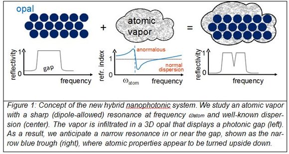
Ever since the early 1900s work of Niels Bohr and Hendrik Lorentz, it is known that atoms display characteristic resonant behavior to light. The hallmark of a resonance is its characteristic peak-trough behavior of the refractive index with optical frequency. Scientists from the Dutch MESA+ Institute for Nano­technology at the University of Twente have recently infiltrated cesium atoms in a self-assembled opal to create a hybrid nanophotonic system. By tuning the opal’s forbidden gap relative to the atomic resonance, dra­matic changes are observed in reflectivity. In the most extreme case, the atomic reflection spectrum is turned upside down[1] compared to the traditional case. Since dispersion is crucial in the control of optical signal pulses, the new results offer opportunities for optical information manipulation. As atoms are exquisite storage de­vices for light quanta, the results open vistas on quantum information processing, as well as on new nanoplasmonics.

A Jan. 12, 2015 MESA+ Institute for Nano­technology at the University of Twente press release, which originated the news item, provides an illustrative diagram and a wealth of technical detail about the research,

Courtesy of the University of Twente

Courtesy of the University of Twente

While the speed of light c is proverbial, it can readily be modified by sending light through a medium with a certain refractive index n. In the medium, the speed will be decreased by the index to c/n. In any material, the refractive index depends on the frequency of the light. Usually the refractive index increases with frequency, called normal dispersion as it prevails at most frequencies in most materials such as a glass of water, a telecom fiber, or an atomic vapor. Close to the resonance frequency of the material, the index strongly decreases, called anomalous dispersion.

Dispersion is essential to control how optical bits of information – encoded as short pulses – is manipulated optical circuits. In modern optics at the nanoscale, called nanophotonics, dispersion is controlled with classes of complex nanostruc­tures that cause novel behavior to emerge. An example is a photonic crystal fiber, which does not consist of only glass like a traditional fiber, but of an intricate arrange­ment of holes and glass nanostructures.

The Twente team led by Harding devised a hybrid system consisting of an atomic vapor infiltrated in an opal photonic crystal. Photonic crystals have attracted considerable attention for their ability to radically control propagation and emission of light. These nanostructures are well-known for their ability to control the emission and propagation of light. The opals have a periodic variation of the refractive index (see Figure 1) that ensures that a certain color of light is forbidden to exist inside the opal. The light cannot enter the opal as it is reflected, which is called a gap (see Figure 1). In an analogy to semiconductors, such an effect is called a “photonic band gap”. Photonic gaps are at the basis of tiny on-chip light sources and lasers, efficient solar cells, invisibility cloaks, and devices to process optical information.

The Twente team changed the index of refraction of the voids in a photonic crystal by substituting the air by a vapor of atoms with a strong resonance, as shown in Figure 1. The contrast of the refractive index between the vapor and the opal’s silica nano­spheres was effectively used as a probe. The density of the cesium vapor was greatly varied by changing the temperature in the cell up to 420 K. At the same time, the photonic gap of the opal shifted relative to the atomic resonance due to a slow chemical reaction between the opal’s backbone material (silica) and the cesium.

On resonance, light excites an atom to a higher state and subsequently the atom reemits the light. Hence, an atom behaves like a little cavity that stores light. Simultaneously the index of refraction changes strongly for colors near resonance. For slightly longer wavelengths the index of refraction is high, on resonance it is close to one, and slightly shorter wavelengths it can even decrease below one. This effect of the cesium atoms is clearly visible in the reflectivity spectra, shown in Figure 2 [not included here], as a sharp increase and decrease of the reflectivity near the atomic resonance. Intriguingly, the characteristic peak-and-trough behavior of atoms (seen at 370 K) was turned upside down at the highest temperature (420 K), where the ce­sium reso­nance was on the red side of the opal’s stopgap.

In nanophotonics, many efforts are currently being devoted to create arrays of nanoresonators in photonic crystals, for exquisite optical signal control on a chip. Unfortunately, however, there is a major challenge in engineering high-quality pho­tonic resonators: they are all different due to inevitable fabrication variations. Hence, it is difficult to tune every resonator in sync. “Our atoms in the opal may be consid­ered as the equivalent of an carefully engineered array of nano-resonators” explains Willem Vos, “Nature takes care that all resonators are all exactly the same. Our hy­brid system solves the variability problem and could perhaps be used to make pho­tonic memories, sensors or switches that are naturally tuned.” And leading Spanish theorist Javier Garcia de Abajo (ICFO) enthuses: “This is a fine and exciting piece of work, initiating the study of atomic resonances with photonic modes in a genuinely new fashion, and suggesting many exciting possibilities, for example through the extension of this study towards combinations with metal nanoplasmonics.”

Here’s a link to and a citation for the paper published in Physical Review B,

Nanophotonic hybridization of narrow atomic cesium resonances and photonic stop gaps of opaline nanostructures by Philip J. Harding, Pepijn W. H. Pinkse, Allard P. Mosk, and Willem L. Vos. Phys. Rev. B 91, 045123 – Published 20 January 2015 DOI: http://dx.doi.org/10.1103/PhysRevB.91.045123

This paper is behind a paywall but there is an earlier iteration of the paper available on the open access arXiv.org website operated by Cornell University,

Nanophotonic hybridization of narrow atomic cesium resonances and photonic stop gaps of opaline nanostructures by Philip J. Harding, Pepijn W.H. Pinkse, Allard P. Mosk, Willem L. Vos. (Submitted on 11 Sep 2014) arXiv:1409.3417

As I understand it, the arXiv.org website is intended to open up access to research and to offer an informal peer review process.

Finally, for anyone who’s nostalgic or perhaps has never heard Diana Ross sing ‘Upside Down’,

Nestling a two-element atomic chain inside a carbon nanotube

While there doesn’t seem to be a short-term application for this research from Japan, the idea of nestling a chain of two elements inside a carbon nanotube is intriguing, from an Oct. 16, 2014 news item on Nanowerk,

Kazutomo Suenaga of the Nanotube Research Center (NTRC) of the National Institute of Advanced Industrial Science and Technology (AIST) and Ryosuke Senga of the Nano-carbon Characterization Team, NTRC, AIST, have synthesized an atomic chain in which two elements are aligned alternately and have evaluated its physical properties on an atomic level.

An ionic crystalline atomic chain of cesium iodine (CsI) has been synthesized by aligning a cesium ion (Cs+), a cation and an iodine ion (I-), an anion, alternately by encapsulating CsI in the microscopic space inside a carbon nanotube. Furthermore, by using an advanced aberration-corrected electron microscope, the physical phenomena unique to the CsI atomic chain, such as the difference in dynamic behavior of its cations and anions, have been discovered. In addition, from theoretical calculation using density functional theory (DFT), this CsI atomic chain has been found to indicate different optical properties from a three-dimensional CsI crystal, and applications to new optical devices are anticipated.

An Oct. 16, 2014 National Institute of Advanced Industrial Science and Technology (AIST) press release, which originated the news item, situates the research within a social and historical context,

Social Background of Research

In the accelerating and ballooning information society, electronic devices used in computers and smartphones has constantly demanded higher performance and efficiency. The materials currently drawing expectations are low-dimensional materials with a single to few-atom width and thickness. Two-dimensional materials, typified by graphene, indicate unique physical characteristics not found in three-dimensional materials, such as its excellent electrical transport properties, and are being extensively researched.

An atomic chain, which has an even finer structure with a width of only one atom, has been predicted to display excellent electrical transport properties, like two-dimensional materials. Although expectations were higher than for two-dimensional materials from the viewpoint of integration, it had attracted little attention until now. This is because of the technological difficulties faced by the various processes of academic research from synthesis to analysis of atomic chains, and academic understanding has not progressed far (Fig. 1).

Figure 1
Figure 1 : Transition of target materials in material research

History of Research

AIST has been developing element analysis methods on a single-atom level to detect certain special structures including impurities, dopants and defects, that affect the properties of low-dimensional materials such as carbon nanotubes and graphene (AIST press releases on July 6, 2009, January 12, 2010, December 16, 2010 and July 9, 2012). In this research, efforts were made for the synthesis and analysis of the atomic chain, a low-dimensional material, using the accumulated technological expertise. This research has been supported by both the Strategic Basic Research Program of the Japan Science and Technology Agency (FY2012 to FY2016), and the Grants-in-aid for Scientific Research of the Japan Society for the Promotion of Science, “Development of elemental technology for the atomic-scale evaluation and application of low-dimensional materials using nano-space” (FY2014 to FY2016).

The press release also offers more details about the research and future applications,

Details of Research

The developed technology is the technology to expose carbon nanotubes, with a diameter of 1 nm or smaller, to CsI vapor to encapsulate CsI in the microscopic space inside the carbon nanotubes, to synthesize an atomic chain in which two elements, Cs and I, are aligned alternately. Furthermore, by combining aberration-corrected electron microscopy and an electronic spectroscopic technique known as electron energy-loss spectroscopy (EELS) detailed structural analysis of this atomic chain was conducted. In order to identify each atom aligned at a distance of 1 nm or less without destroying them, the accelerating voltage of the electron microscope was significantly lowered to 60 kV to reduce damage to the sample by electron beams, while maintaining sufficient spatial resolution of around 1 nm. Figure 2 indicates the smallest CsI crystal confirmed so far, and the CsI atomic chain synthesized in this research.

Figure 2
Figure 2 : Comparison of CsI atomic chain and CsI crystal
(Top: Actual annular dark-field images, Bottom: Corresponding models)

Figure 3 shows the annular dark-field (ADF) image of the CsI atomic chain and the element mapping for Cs and I, respectively, obtained by EELS. It can be seen that the two elements are aligned alternately. There has not been any report of this simple and ideal structure actually being produced and observed, and it can be said to be a fundamental, important finding in material science.

Normally, in an ADF image, those with larger atomic numbers appear brighter. However, in this CsI atomic chain, I (atomic number 53) appears brighter than Cs (atomic number 55). This is because Cs, being a cation, moves more actively (more accurately, the total amount of electrons scattered by the Cs atom is not very different from those of the I atom, but the electrons scattered by the moving Cs atom generate spatial expansion), indicating a difference in dynamic behavior of the cation and the anion that cannot occur in a large three-dimensional crystal. Locations where single Cs atom or I atom is absent, namely vacancies, were also found (Fig. 3, right).

The unique behavior and structure influence various physical properties. When optical absorption spectra were calculated using DFT, the response of the CsI atomic chain to light differed with the direction of incidence. Furthermore, it was found that in a CsI atomic chain with vacancies, the electron state of vacancy sites where the I atom is absent possess a donor level at which electrons were easily released, while vacancy sites where the Cs atom is absent possess a receptor level at which electrons were easily received. By making use of these physical properties, applications to new electro-optical devices, such as a micro-light source and an optical switch using light emission from a single vacancy in the CsI atomic chain, are conceivable. In addition, further research into combinations of other elements triggered by the present results may lead to the development of new materials and device applications. There are expectations for atomic chains to be the next-generation materials for devices in search of further miniaturization and integration.

Figure 3
Figure 3 : Synthesized CsI atomic chain, encapsulated in double-walled carbon nanotube
(From left: ADF image, element maps for Cs and I, model, ADF image of CsI atomic chains with vacancies)

Future Plans

Since the CsI atomic chain displays optical properties significantly different from large crystals that can be seen by the human eye, there are expectations for its application for new electro-optical devices such as a micro-light source and an optical switch using light emission from a single vacancy in the CsI atomic chain. The researchers will conduct experimental research in its application, focused on detailed study of its various physical properties, starting with its optical properties. In addition to CsI, efforts will also be made in the development of new materials that combine various elements, by applying this technology to other materials.

Furthermore, the mechanism of all adsorbents of radioactive substances (carbon nanotubes, zeolite, Prussian blue, etc.) currently being developed for commercial use are methods of encapsulating radioactive atoms inside microscopic space in the material. The researchers hope to utilize the knowledge of the behavior of the Cs atom in a microscopic space obtained in this research, to improve adsorption performance.

Here’s a link to and a citation for the research paper,

Atomic structure and dynamic behaviour of truly one-dimensional ionic chains inside ​carbon nanotubes by Ryosuke Senga, Hannu-Pekka Komsa, Zheng Liu, Kaori Hirose-Takai, Arkady V. Krasheninnikov, & Kazu Suenaga. Nature Materials (2014) doi:10.1038/nmat4069 Published online 14 September 2014

This paper is behind a paywall.