Tag Archives: Chalmers University of Technology

Substituting graphene and other carbon materials for scarce metals

A Sept. 19, 2017 news item on Nanowerk announces a new paper from the Chalmers University of Technology (Sweden), the lead institution for the Graphene Flagship (a 1B Euro 10 year European Commission programme), Note: A link has been removed,

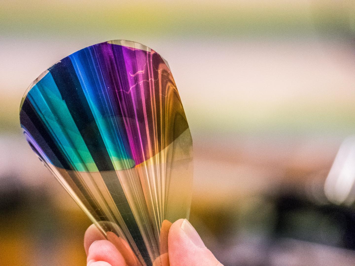
Scarce metals are found in a wide range of everyday objects around us. They are complicated to extract, difficult to recycle and so rare that several of them have become “conflict minerals” which can promote conflicts and oppression. A survey at Chalmers University of Technology now shows that there are potential technology-based solutions that can replace many of the metals with carbon nanomaterials, such as graphene (Journal of Cleaner Production, “Carbon nanomaterials as potential substitutes for scarce metals”).

They can be found in your computer, in your mobile phone, in almost all other electronic equipment and in many of the plastics around you. Society is highly dependent on scarce metals, and this dependence has many disadvantages.

A Sept. 19, 2017 Chalmers University of Technology press release by Ulrika Ernstrom,, which originated the news item, provides more detail about the possibilities,

They can be found in your computer, in your mobile phone, in many of the plastics around you and in almost all electronic equipment. Society is highly dependent on scarce metals, and this dependence has many disadvantages.
Scarce metals such as tin, silver, tungsten and indium are both rare and difficult to extract since the workable concentrations are very small. This ensures the metals are highly sought after – and their extraction is a breeding ground for conflicts, such as in the Democratic Republic of the Congo where they fund armed conflicts.
In addition, they are difficult to recycle profitably since they are often present in small quantities in various components such as electronics.
Rickard Arvidsson and Björn Sandén, researchers in environmental systems analysis at Chalmers University of Technology, have now examined an alternative solution: substituting carbon nanomaterials for the scarce metals. These substances – the best known of which is graphene – are strong materials with good conductivity, like scarce metals.
“Now technology development has allowed us to make greater use of the common element carbon,” says Sandén. “Today there are many new carbon nanomaterials with similar properties to metals. It’s a welcome new track, and it’s important to invest in both the recycling and substitution of scarce metalsfrom now on.”
The Chalmers researchers have studied  the main applications of 14 different metals, and by reviewing patents and scientific literature have investigated the potential for replacing them by carbon nanomaterials. The results provide a unique overview of research and technology development in the field.
According to Arvidsson and Sandén the summary shows that a shift away from the use of scarce metals to carbon nanomaterials is already taking place.
….
“There are potential technology-based solutions for replacing 13 out of the 14 metals by carbon nanomaterials in their most common applications. The technology development is at different stages for different metals and applications, but in some cases such as indium and gallium, the results are very promising,” Arvidsson says.
“This offers hope,” says Sandén. “In the debate on resource constraints, circular economy and society’s handling of materials, the focus has long been on recycling and reuse. Substitution is a potential alternative that has not been explored to the same extent and as the resource issues become more pressing, we now have more tools to work with.”
The research findings were recently published in the Journal of Cleaner Production. Arvidsson and Sandén stress that there are significant potential benefits from reducing the use of scarce metals, and they hope to be able to strengthen the case for more research and development in the field.
“Imagine being able to replace scarce metals with carbon,” Sandén says. “Extracting the carbon from biomass would create a natural cycle.”
“Since carbon is such a common and readily available material, it would also be possible to reduce the conflicts and geopolitical problems associated with these metals,” Arvidsson says.
At the same time they point out that more research is needed in the field in order to deal with any new problems that may arise if the scarce metals are replaced.
“Carbon nanomaterials are only a relatively recent discovery, and so far knowledge is limited about their environmental impact from a life-cycle perspective. But generally there seems to be a potential for a low environmental impact,” Arvidsson says.

FACTS AND MORE INFORMATION

Carbon nanomaterials consist solely or mainly of carbon, and are strong materials with good conductivity. Several scarce metals have similar properties. The metals are found, for example, in cables, thin screens, flame-retardants, corrosion protection and capacitors.
Rickard Arvidsson and Björn Sandén at Chalmers University of Technology have investigated whether the carbon nanomaterials graphene, fullerenes and carbon nanotubes have the potential to replace 14 scarce metals in their main areas of application (see table). They found potential technology-based solutions to replace the metals with carbon nanomaterials for all applications except for gold in jewellery. The metals which we are closest to being able to substitute are indium, gallium, beryllium and silver.

Here’s a link to and a citation for the paper,

Carbon nanomaterials as potential substitutes for scarce metals by Rickard Arvidsson, Björn A. Sandén. Journal of Cleaner Production (0959-6526). Vol. 156 (2017), p. 253-261. DOI: https://doi.org/10.1016/j.jclepro.2017.04.048

This paper appears to be open access.

Colours in bendable electronic paper

Scientists at Chalmers University of Technology (Sweden) are able to produce a rainbow of colours in a new electronic paper according to an Oct. 14, 2016 news item on Nanowerk,

Less than a micrometre thin, bendable and giving all the colours that a regular LED display does, it still needs ten times less energy than a Kindle tablet. Researchers at Chalmers University of Technology have developed the basis for a new electronic “paper.”

When Chalmers researcher Andreas Dahlin and his PhD student Kunli Xiong were working on placing conductive polymers on nanostructures, they discovered that the combination would be perfectly suited to creating electronic displays as thin as paper. A year later the results were ready for publication. A material that is less than a micrometre thin, flexible and giving all the colours that a standard LED display does.

An Oct. 14, 2016 Chalmers University of Technology press release (also on EurekAlert) by Mats Tiborn, which originated the news item, expands on the theme,

“The ’paper’ is similar to the Kindle tablet. It isn’t lit up like a standard display, but rather reflects the external light which illuminates it. Therefore it works very well where there is bright light, such as out in the sun, in contrast to standard LED displays that work best in darkness. At the same time it needs only a tenth of the energy that a Kindle tablet uses, which itself uses much less energy than a tablet LED display”, says Andreas Dahlin.

It all depends on the polymers’ ability to control how light is absorbed and reflected. The polymers that cover the whole surface lead the electric signals throughout the full display and create images in high resolution. The material is not yet ready for application, but the basis is there. The team has tested and built a few pixels. These use the same red, green and blue (RGB) colours that together can create all the colours in standard LED displays. The results so far have been positive, what remains now is to build pixels that cover an area as large as a display.

“We are working at a fundamental level but even so, the step to manufacturing a product out of it shouldn’t be too far away. What we need now are engineers”, says Andreas Dahlin.

One obstacle today is that there is gold and silver in the display.

“The gold surface is 20 nanometres thick so there is not that much gold in it. But at present there is a lot of gold wasted in manufacturing it. Either we reduce the waste or we find another way to reduce the production cost”, says Andreas Dahlin.

Caption: Chalmers' e-paper contains gold, silver and PET plastic. The layer that produces the colours is less than a micrometre thin. Credit: Mats Tiborn

Caption: Chalmers’ e-paper contains gold, silver and PET plastic. The layer that produces the colours is less than a micrometre thin. Credit: Mats Tiborn

Here’s a link to and a citation for the paper,

Plasmonic Metasurfaces with Conjugated Polymers for Flexible Electronic Paper in Color by Kunli Xiong, Gustav Emilsson, Ali Maziz, Xinxin Yang, Lei Shao, Edwin W. H. Jager, and Andreas B. Dahlin. Advanced Materials DOI: 10.1002/adma.201603358 Version of Record online: 27 SEP 2016

© 2016 WILEY-VCH Verlag GmbH & Co. KGaA, Weinheim

This paper is behind a paywall.

Finally, Dexter Johnson in an Oct. 18, 2016 posting on his Nanoclast blog (on the IEEE [Institute of Electrical and Electronics Engineers] website) offers some broader insight into this development (Note: Links have been removed),

Plasmonic nanostructures leverage the oscillations in the density of electrons that are generated when photons hit a metal surface. Researchers have used these structures for applications including increasing the light absorption of solar cells and creating colors without the need for dyes. As a demonstration of how effective these nanostructures are as a replacement for color dyes, a the technology has been used to produce a miniature copy of the Mona Lisa in a space smaller than the footprint taken up by a single pixel on an iPhone Retina display.

Man with world’s first implanted bionic arm participates in first Cybathlon (olympics for cyborgs)

The world’s first Cybathlon is being held on Oct. 8, 2016 in Zurich, Switzerland. One of the participants is an individual who took part in some groundbreaking research into implants which was featured in my Oct. 10, 2014 posting. There’s more about the Cybathlon and the participant in an Oct. 4, 2016 news item on phys.org,

A few years ago, a patient was implanted with a bionic arm for the first time in the world using control technology developed at Chalmers University of Technology. He is now taking part in Cybathlon, a new international competition in which 74 participants with physical disabilities will compete against each other, using the latest robotic prostheses and other assistive technologies – a sort of ‘Cyborg Olympics’.

The Paralympics will now be followed by the Cybathlon, which takes place in Zürich on October 8th [2016]. This is the first major competition to show that the boundaries between human and machine are becoming more and more blurred. The participants will compete in six different disciplines using the machines they are connected to as well as possible.

Cybathlon is intended to drive forward the development of prostheses and other types of assistive aids. Today, such technologies are often highly advanced technically, but provide limited value in everyday life.

An Oct. 4, 2016 Chalmers University of Technology press release by Johanna Wilde, which originated the news item, provides details about the competitor, his prosthetic device, and more,

Magnus, one of the participants, has now had his biomechatronically integrated arm prosthesis for almost four years. He says that his life has totally changed since the implantation, which was performed by Dr Rickard Brånemark, associate professor at Sahlgrenska University Hospital.

“I don’t feel handicapped since I got this arm”, says Magnus. “I can now work full time and can perform all the tasks in both my job and my family life. The prosthesis doesn’t feel like a machine, but more like my own arm.”

Magnus lives in northern Sweden and works as a lorry driver. He regularly visits Gothenburg in southern Sweden and carries out tests with researcher Max Ortiz Catalan, assistant professor at Chalmers University of Technology, who has been in charge of developing the technology and leads the team competing in the Cybathlon.

“This is a completely new research field in which we have managed to directly connect the artificial limb to the skeleton, nerves and muscles,” says Dr Max Ortiz Catalan. “In addition, we are including direct neural sensory feedback in the prosthetic arm so the patient can intuitively feel with it.”

Today Magnus can feel varying levels of pressure in his artificial hand, something which is necessary to instinctively grip an object firmly enough. He is unique in the world in having a permanent sensory connection between the prosthesis and his nervous system, working outside laboratory conditions. Work is now under way to add more types of sensations.

At the Cybathlon he will be competing for the Swedish team, which is formed by Chalmers University of Technology, Sahlgrenska University Hospital and the company Integrum AB.

The competition has a separate discipline for arm prostheses. In this discipline Magnus has to complete a course made up of six different stations at which the prosthesis will be put to the test. For example, he has to open a can with a can opener, load a tray with crockery and open a door with the tray in his hand. The events at the Cybathlon are designed to be spectator-friendly while being based on various operations that the participants have to cope with in their daily lives.

“However, the competition will not really show the unique advantages of our technology, such as the sense of touch and the bone-anchored attachment which makes the prosthesis comfortable enough to wear all day,” says Max Ortiz Catalan.

Magnus is the only participant with an amputation above the elbow. This naturally makes the competition more difficult for him than for the others, who have a natural elbow joint.

“From a competitive perspective Cybathlon is far from ideal to demonstrate clinically viable technology,” says Max Ortiz Catalan. “But it is a major and important event in the human-machine interface field in which we would like to showcase our technology. Unlike several of the other participants, Magnus will compete in the event using the same technology he uses in his everyday life.”

Facts about Cybathlon
•    The very first Cybathlon is being organised by the Swiss university ETH Zürich.
•    The €5 million event will take place in Zürich´s 7600 spectator ice hockey stadium, Swiss Arena.
•    74 participants are competing for 59 different teams from 25 countries around the world. In total, the teams consist of about 300 scientists, engineers, support staff and competitors.
•    The teams range from small ad hoc teams to the world’s largest manufacturers of advanced prostheses.
•    The majority of the teams are groups from research labs and many of the prostheses have come straight out of the lab.
•    Unlike the Olympics and Paralympics, the Cybathlon participants are not athletes but ordinary people with various disabilities. The aims of the competition are to establish a dialogue between academia and industry, to facilitate discussion between technology developers and people with disabilities and to promote the use of robotic assistive aids to the general public.
•    Cybathlon will return in 2020, as a seven-day event in Tokyo, to coincide with the Olympics.

Facts about the Swedish team
The Opra Osseointegration team is a multidisciplinary team comprising technical and medical partners. The team is led by Dr Max Ortiz Catalan, assistant professor at Chalmers University of Technology, who has been in charge of developing the technology in close collaboration with Dr Rickard Brånemark, who is a surgeon at Sahlgrenska University Hospital and an associate professor at Gothenburg University. Dr Brånemark led the team performing the implantation of the device. Integrum AB, a Swedish company, complements the team as the pioneering provider of bone-anchored limb prostheses.

This video gives you an idea of what it’s in store on Oct. 8, 2016,

Dissipating heat with graphene-based film

As the summer approaches here in the Northern Hemisphere I think longingly of frost and snow and so readers may find more than the usual number of stories about ‘cooling’. On that note, Chalmers Technical University (Sweden) is announcing some new research into cooling graphene-based films, from an April 29, 2016 news item on ScienceDaily,

Heat dissipation in electronics and optoelectronics is a severe bottleneck in the further development of systems in these fields. To come to grips with this serious issue, researchers at Chalmers University of Technology have developed an efficient way of cooling electronics by using functionalized graphene nanoflakes. …

“Essentially, we have found a golden key with which to achieve efficient heat transport in electronics and other power devices by using graphene nanoflake-based film. This can open up potential uses of this kind of film in broad areas, and we are getting closer to pilot-scale production based on this discovery,” says Johan Liu, Professor of Electronics Production at Chalmers University of Technology in Sweden.

An April 29, 2016 Chalmers Technical University press release (also on EurekAlert), which originated the news item, describes the work in more detail,

The researchers studied the heat transfer enhancement of the film with different functionalized amino-based and azide-based silane molecules, and found that the heat transfer efficiency of the film can be improved by over 76 percent by introducing functionalization molecules, compared to a reference system without the functional layer. This is mainly because the contact resistance was drastically reduced by introducing the functionalization molecules.

Meanwhile, molecular dynamic simulations and ab initio calculations reveal that the functional layer constrains the cross-plane scattering of low-frequency phonons, which in turn enhances in-plane heat-conduction of the bonded film by recovering the long flexural phonon lifetime. The results suggested potential thermal management solutions for electronic devices.

In the research, scientists studied a number of molecules that were immobilized at the interfaces and at the edge of graphene nanoflake-based sheets forming covalent bonds. They also probed interface thermal resistance by using a photo-thermal reflectance measurement technique to demonstrate an improved thermal coupling due to functionalization.

“This is the first time that such systematic research has been done. The present work is much more extensive than previously published results from several involved partners, and it covers more functionalization molecules and also more extensive direct evidence of the thermal contact resistance measurement,” says Johan Liu.

Here’s a link to and a citation for the paper,

Functionalization mediates heat transport in graphene nanoflakes by Haoxue Han, Yong Zhang, Nan Wang, Majid Kabiri Samani, Yuxiang Ni, Zainelabideen Y. Mijbil, Michael Edwards, Shiyun Xiong, Kimmo Sääskilahti, Murali Murugesan, Yifeng Fu, Lilei Ye, Hatef Sadeghi, Steven Bailey, Yuriy A. Kosevich, Colin J. Lambert, Johan Liu, & Sebastian Volz. Nature Communications 7, Article number: 11281  doi:10.1038/ncomms11281 Published 29 April 2016

This is an open access paper.

With over 150 partners from over 20 countries, the European Union’s Graphene Flagship research initiative unveils its work package devoted to biomedical technologies

An April 11, 2016 news item on Nanowerk announces the Graphene Flagship’s latest work package,

With a budget of €1 billion, the Graphene Flagship represents a new form of joint, coordinated research on an unprecedented scale, forming Europe’s biggest ever research initiative. It was launched in 2013 to bring together academic and industrial researchers to take graphene from the realm of academic laboratories into European society in the timeframe of 10 years. The initiative currently involves over 150 partners from more than 20 European countries. The Graphene Flagship, coordinated by Chalmers University of Technology (Sweden), is implemented around 15 scientific Work Packages on specific science and technology topics, such as fundamental science, materials, health and environment, energy, sensors, flexible electronics and spintronics.

Today [April 11, 2016], the Graphene Flagship announced in Barcelona the creation of a new Work Package devoted to Biomedical Technologies, one emerging application area for graphene and other 2D materials. This initiative is led by Professor Kostas Kostarelos, from the University of Manchester (United Kingdom), and ICREA Professor Jose Antonio Garrido, from the Catalan Institute of Nanoscience and Nanotechnology (ICN2, Spain). The Kick-off event, held in the Casa Convalescència of the Universitat Autònoma de Barcelona (UAB), is co-organised by ICN2 (ICREA Prof Jose Antonio Garrido), Centro Nacional de Microelectrónica (CNM-IMB-CSIC, CIBER-BBN; CSIC Tenured Scientist Dr Rosa Villa), and Institut d’Investigacions Biomèdiques August Pi i Sunyer (IDIBAPS; ICREA Prof Mavi Sánchez-Vives).

An April 11, 2016 ICN2 press release, which originated the news item, provides more detail about the Biomedical Technologies work package and other work packages,

The new Work Package will focus on the development of implants based on graphene and 2D-materials that have therapeutic functionalities for specific clinical outcomes, in disciplines such as neurology, ophthalmology and surgery. It will include research in three main areas: Materials Engineering; Implant Technology & Engineering; and Functionality and Therapeutic Efficacy. The objective is to explore novel implants with therapeutic capacity that will be further developed in the next phases of the Graphene Flagship.

The Materials Engineering area will be devoted to the production, characterisation, chemical modification and optimisation of graphene materials that will be adopted for the design of implants and therapeutic element technologies. Its results will be applied by the Implant Technology and Engineering area on the design of implant technologies. Several teams will work in parallel on retinal, cortical, and deep brain implants, as well as devices to be applied in the periphery nerve system. Finally, The Functionality and Therapeutic Efficacy area activities will centre on development of devices that, in addition to interfacing the nerve system for recording and stimulation of electrical activity, also have therapeutic functionality.

Stimulation therapies will focus on the adoption of graphene materials in implants with stimulation capabilities in Parkinson’s, blindness and epilepsy disease models. On the other hand, biological therapies will focus on the development of graphene materials as transport devices of biological molecules (nucleic acids, protein fragments, peptides) for modulation of neurophysiological processes. Both approaches involve a transversal innovation environment that brings together the efforts of different Work Packages within the Graphene Flagship.

A leading role for Barcelona in Graphene and 2D-Materials

The kick-off meeting of the new Graphene Flagship Work Package takes place in Barcelona because of the strong involvement of local institutions and the high international profile of Catalonia in 2D-materials and biomedical research. Institutions such as the Catalan Institute of Nanoscience and Nanotechnology (ICN2) develop frontier research in a supportive environment which attracts talented researchers from abroad, such as ICREA Research Prof Jose Antonio Garrido, Group Leader of the ICN2 Advanced Electronic Materials and Devices Group and now also Deputy Leader of the Biomedical Technologies Work Package. Until summer 2015 he was leading a research group at the Technische Universität München (Germany).

Further Graphene Flagship events in Barcelona are planned; in May 2016 ICN2 will also host a meeting of the Spintronics Work Package. ICREA Prof Stephan Roche, Group Leader of the ICN2 Theoretical and Computational Nanoscience Group, is the deputy leader of this Work Package led by Prof Bart van Wees, from the University of Groningen (The Netherlands). Another Work Package, on optoelectronics, is led by Prof Frank Koppens from the Institute of Photonic Sciences (ICFO, Spain), with Prof Andrea Ferrari from the University of Cambridge (United Kingdom) as deputy. Thus a number of prominent research institutes in Barcelona are deeply involved in the coordination of this European research initiative.

Kostas Kostarelos, the leader of the Biomedical Technologies Graphene Flagship work package, has been mentioned here before in the context of his blog posts for The Guardian science blog network (see my Aug. 7, 2014 post for a link to his post on metaphors used in medicine).

Explaining research into matching plasmonic nanoantenna resonances with atoms, molecules, and quantum dots

There’s a very nice explanation of the difficulties associeated with using plasmonic nanoantennas as sensors in a March 21, 2016 news item on phys.org,

Plasmonic nanoantennas are among the hot topics in science at the moment because of their ability to interact strongly with light, which for example makes them useful for different kinds of sensing. But matching their resonances with atoms, molecules or so called quantum dots has been difficult so far because of the very different length scales involved. Thanks to a grant from the Engkvist foundation, Timur Shegai, assistant professor at Chalmers University of Technology, hopes to find a way to do this and by that open doors for applications such as safe long distance communication channels.

A molecule being illuminated by two gold nanoantennas. By: Alexander Ericson Courtesy: Chalmers University of Technology

A molecule being illuminated by two gold nanoantennas. By: Alexander Ericson Courtesy: Chalmers University of Technology

The image, looking like a stylized butterfly or bow tie, above accompanies Karin Weijdegård’s March ??, 2016 Chalmers University of Technology press release, which originated the news item, expands on the research theme,

The diffraction limit makes it very hard for light to interact with the very smallest particles or so called quantum systems such as atoms, molecules or quantum dots. The size of such a particle is simply so much smaller than the wavelength of light that there cannot be a strong interaction between the two. But by using plasmonic nanoantennas, which can be described as metallic nanostructures that are able to focus light very strongly and in wavelengths smaller than those of the visible light, one can build a bridge between the light and the atom, molecule or quantum dot and that is what Timur Shegai is working on.

“Plasmonic nanostructures are themselves smaller than wavelengths of light, but because they have a lot of free electrons they can store the electromagnetic energy in a volume which is actually a lot smaller than the diffraction limit, which helps to bridge the gap between really small objects such as molecules and the larger wavelengths of light,” he says.

Matching the harmonic with the un-harmonic

This might sound easy enough, but the problem with combining the two is that they behave in very different ways. The behaviour of plasmonic nanostructures is very linear, like a harmonic oscillator it will regularly move from side to side no matter how much energy or in other words how many excitations are stored in it. On the other hand, so called quantum systems like atoms, molecules or quantum dots are very much the opposite – their optical properties are highly un-harmonic. Here it makes a big difference if you excite the system with one or two or hundreds of photons.

“Now imagine that you couple together this un-harmonic resonator and a harmonic resonator, and add the possibility to interact with light much stronger than the un-harmonic system alone would have allowed. That opens up very interesting possibilities for quantum technologies and for non-linear optics for example. But as opposed to previous attempts that have been done at very low temperatures and in a vacuum, we will do it at room temperature.”

Communication channels impossible to hack

One possible application where this technology could be useful in the future is to create channels for long distance communications that are impossible to hack. With the current technology this kind of safe communication is only possible if the persons communicating is within a distance of about one hundred kilometres from each other, because that is the maximum distance that an individual photon can run in fibres before it scatters and the signal is lost.

“The kind of ultra small and ultra fast technology we want to develop could be useful in a so called quantum repeater, a device that could be installed across the line from for example New York to London, that would repeat the photon every time it is about to be scattered,” says Timur Shegai.

At the moment though, it is the fundamental aspects of merging plasmons with quantum systems that interest Timur Shegai. To be able to experimentally prove that the there can be interactions between the two systems, he first of all needs to fabricate model systems at the nano level. This is a big challenge, but with the grant of 1,6 million SEK over a period of two years that he just received from the Engkvist foundation, the chances of success have improved.

“Since I am a researcher at the beginning of my career every person is a huge improvement and now I can hire a post doc to work with my group. This means that the project can be divided into sub parts and together we will be able to explore more possibilities about this new technology.”

Thank you Karin Weijdegård for the explanation.

Tiny, electrically conductive 3D-printed chair made from cellulose

Sweden’s Chalmers University of Technology researchers have just announced that they’ve printed a very small 3D chair with electrical properties using cellulose nanomaterials. From a June 17, 2015 news item on Nanowerk,

A group of researchers at Chalmers University of Technology have managed to print and dry three-dimensional objects made entirely by cellulose for the first time with the help of a 3D-bioprinter. They also added carbon nanotubes to create electrically conductive material. The effect is that cellulose and other raw material based on wood will be able to compete with fossil-based plastics and metals in the on-going additive manufacturing revolution, which started with the introduction of the 3D-printer.

Here’s the 3D-printed chair,

The tiny chair made of cellulose is a demonstrational object, printed using the 3D bioprinter at Chalmers University of Technology. Photo: Peter Widing

The tiny chair made of cellulose is a demonstrational object, printed using the 3D bioprinter at Chalmers University of Technology. Photo: Peter Widing

A June 17, 2015 Chalmers University of Technology press release (also on EurekAlert*), which originated the news item, describes the problem with printing from cellulose nanomaterials and how it was solved,

The difficulty using cellulose in additive manufacturing is that cellulose does not melt when heated. Therefore, the 3D printers and processes designed for printing plastics and metals cannot be used for materials like cellulose. The Chalmers researchers solved this problem by mixing cellulose nanofibrils in a hydrogel consisting of 95-99 percent water. The gel could then in turn be dispensed with high fidelity into the researchers’ 3D bioprinter, which was earlier used to produce scaffolds for growing cells, where the end application is patient-specific implants.

The next challenge was to dry the printed gel-like objects without them losing their three-dimensional shape.

“The drying process is critical,” Paul Gatenholm explains. “We have developed a process in which we freeze the objects and remove the water by different means as to control the shape of the dry objects. It is also possible to let the structure collapse in one direction, creating thin films.”

Furthermore, the cellulose gel was mixed with carbon nanotubes to create electrically conductive ink after drying. Carbon nanotubes conduct electricity, and another project at Wallenberg Wood Science Center aims at developing carbon nanotubes using wood.

Using the two gels together, one conductive and one non-conductive, and controlling the drying process, the researchers produced three-dimensional circuits, where the resolution increased significantly upon drying.

The two gels together provide a basis for the possible development of a wide range of products made by cellulose with in-built electric currents.

“Potential applications range from sensors integrated with packaging, to textiles that convert body heat to electricity, and wound dressings that can communicate with healthcare workers,” says Paul Gatenholm. “Our research group now moves on with the next challenge, to use all wood biopolymers, besides cellulose.”

The research findings are presented this week at the conference New Materials From Trees that takes place in Stockholm, Sweden, June 15-17 [2015].

The research team members are Ida Henriksson, Cristina de la Pena, Karl Håkansson, Volodymyr Kuzmenko and Paul Gatenholm at Chalmers University of Technology.

This research reminds me of another effort, a computer chip fashioned of cellulose nanofibrils (CNF) from the University of Wisconsin-Madison (mentioned in my May 27, 2015 post).

* EurekAlert link added June 18, 2015.

A use for fullerenes—inside insulation plastic for high-voltage cables

A Jan. 27, 2015 news item on Nanowerk, describes research which suggests that there may a new use for buckminsterfullerenes (or what they’re calling ‘carbon nanoballs’),

Researchers at Chalmers University of Technology [Sweden] have discovered that the insulation plastic used in high-voltage cables can withstand a 26 per cent higher voltage if nanometer-sized carbon balls are added. This could result in enormous efficiency gains in the power grids of the future, which are needed to achieve a sustainable energy system.

The renewable energy sources of tomorrow will often be found far away from the end user. Wind turbines, for example, are most effective when placed out at sea. Solar energy will have the greatest impact on the European energy system if focus is on transport of solar power from North Africa and Southern Europe to Northern Europe.

“Reducing energy losses during electric power transmission is one of the most important factors for the energy systems of the future,” says Chalmers researcher Christian Müller. “The other two are development of renewable energy sources and technologies for energy storage.”

The Jan. 27, 2015 Chalmers University of Technology press release (also on EurekAlert) by Johanna Wilde, which originated the news item, provides more information about the research,

Together with colleagues from Chalmers and the company Borealis in Stenungsund, he [Müller] has found a powerful method for reducing energy losses in alternating current cables.  The results were recently published in Advanced Materials, a highly ranked scientific journal.

The researchers have shown that different variants of the C60 carbon ball, a nanomaterial in the fullerene molecular group, provide strong protection against breakdown of the insulation plastic used in high-voltage cables. Today the voltage in the cables has to be limited to prevent the insulation layer from getting damaged. The higher the voltage the more electrons can leak out into the insulation material, a process which leads to breakdown.

It is sufficient to add very small amounts of fullerene to the insulation plastic for it to withstand a voltage that is 26 per cent higher, without the material breaking down, than the voltage that plastic without the additive can withstand.

“Being able to increase the voltage to this extent would result in enormous efficiency gains in power transmission all over the world,” says Christian Müller. “A major issue in the industry is how transmission efficiency can be improved without making the power cables thicker, since they are already very heavy and difficult to handle.”

Using additives to protect the insulation plastic has been a known concept since the 1970s, but until now it has been unknown exactly what and how much to add. Consequently, additives are currently not used at all for the purpose, and the insulation material is manufactured with the highest possible degree of chemical purity.

In recent years, other researchers have experimented with fullerenes in the electrically conductive parts of high-voltage cables. Until now, though, it has been unknown that the substance can be beneficial for the insulation material.

The Chalmers researchers have now demonstrated that fullerenes are the best voltage stabilizers identified for insulation plastic thus far. This means they have a hitherto unsurpassed ability to capture electrons and thus protect other molecules from being destroyed by the electrons.

To arrive at these findings, the researchers tested a number of molecules that are also used within organic solar cell research at Chalmers. The molecules were tested using several different methods, and were added to pieces of insulation plastic used for high-voltage cables. The pieces of plastic were then subjected to an increasing electric field until they crackled. Fullerenes turned out to be the type of additive that most effectively protects the insulation plastic.

The press release includes some facts about buckyballs or buckminsterfullerenes or fullerenes or C60 or carbon nanoballs, depending on what you want to call them,

 Facts: Carbon ball C60

  • The C60 carbon ball is also called buckminsterfullerene. It consists of 60 carbon atoms that are placed so that the molecule resembles a nanometer-sized football. C60 is included in the fullerene molecular class.
  • Fullerenes were discovered in 1985, which resulted in the Nobel Prize in Chemistry in 1996. They have unique electronic qualities and have been regarded as very promising material for several applications. Thus far, however, there have been few industrial usage areas.
  • Fullerenes are one of the five forms of pure carbon that exist. The other four are graphite, graphene/carbon nanotubes, diamond and amorphous carbon, for example soot.

Here’s a link to and a citation for the research paper,

A New Application Area for Fullerenes: Voltage Stabilizers for Power Cable Insulation by Markus Jarvid, Anette Johansson, Renee Kroon, Jonas M. Bjuggren, Harald Wutzel, Villgot Englund, Stanislaw Gubanski, Mats R. Andersson, and Christian Müller. Advanced Materials DOI: 10.1002/adma.201404306 Article first published online: 12 DEC 2014

© 2014 WILEY-VCH Verlag GmbH & Co. KGaA, Weinheim

This paper is behind a paywall.

Here’s an image of wind turbines, an example of equipment which could benefit greatly from better insulation.,

Images: Lina Bertling, Jan-Olof Yxell, Carolina Eek Jaworski, Anette Johansson, Markus Jarvid, Christian Müller

Images: Lina Bertling, Jan-Olof Yxell, Carolina Eek Jaworski, Anette Johansson, Markus Jarvid, Christian Müller

You can find this image and others by clicking on the Chalmers University press release link (assuming the page hasn’t been moved). You can find more information about Borealis (the company Müller is working with) here.

Chalmers University gears up to offer Graphene Science and Technology, an online, international course

They’ll be offering a MOOC, massive open online course, at Chalmers University of Technology, Sweden, on the topic of graphene starting March 23, 2015 according a Nov. 21, 2014 news item on Nanowerk,

Starting in 2015, Chalmers University of Technology in Sweden will be a global disseminator of knowledge. The beginning of the year will mark the start of ChalmersX – the venture of Chalmers moocs on the platform edx.org.

Chalmers announces its membership in edx at the ongoing conference Edx Global Forum in Boston. Edx is the platform where Chalmers’ moocs will be accessible. Universities such as MIT, Harvard, UC Berkeley, the University of Tokyo and many more offer their moocs on the same platform.

“This is a new and different way for us to take on the role of knowledge disseminator in our society“, says Maria Knutson Wedel, vice president for undergraduate and master’s education at Chalmers.

With a computer and an Internet connection, course participants all over the world can watch video lectures, take part in discussions, do assignments and take exams.

“Previously, we have primarily shared knowledge on a local and national level. The technology today enables global knowledge sharing – we can reach people who need the knowledge in question no matter where they are located in the world,“ says Maria Knutson Wedel.

A Nov. 21, 2014 Chalmers University press release on mydesk.com, which seems to have originated the news item, notes that the university is the consortium lead on the European Union’s Graphene Flagship project,

The first ChalmersX mooc will be an introduction to the super-material graphene: Introduction to Graphene Science and Technology. The subject is at the forefront of research, and EU’s biggest research initiative ever – Graphene Flagship – is based at Chalmers.

The course is led by graphene researcher Jie Sun. He took the initiative to the mooc as he saw the need of large-scale education about graphene.

“I hope to give the participants of the course basic knowledge of graphene. At the end of the course, an engineer should be able to determine if graphene is suitable for the company’s products, and a student should be able to decide if the subject is of interest for continued studies”, says Jie Sun.

Moocs are a growing trend in higher education. There is a great deal of interest in the courses – each one typically attracts tens of thousands of participants.

Maria Knutson Wedel believes that moocs can be very useful as supplementary or continuing professional development for people who are already part of working life. She does not believe that the courses can completely replace a traditional campus education, however. Campus education are closely connected and designed to correspond to the expectations from industry, for example. This type of education also results in a degree and a title, something which companies consider when hiring.

“However, this probably depends in part on traditional thinking on the part of the people who do the hiring at companies. In the future, we may reach a point that knowledge, regardless of how it has been obtained, becomes more important than certificates and grades,“ says Maria Knutson Wedel.

The ChalmersX moocs will be specially adapted to their context – the recordings will not consist of traditional 45-minute lectures. The teachers who have developed the course have carefully analysed the concepts they want participants to come away with after the course. The content is then boiled down to short video clips of 5-7 minutes each.

The next mooc in line after the course on graphene will be on sustainability in everyday life, starting in May 2015.

More about: Moocs

Moocs, an abbreviation of massive open online courses, are online courses aimed at unlimited participation and open access via the web. The term mooc was coined in 2008. As opposed to traditional distance learning, moocs do not have any prerequisites for admission. Exams are conducted by machine and there are platforms on which participants can get in contact with each other and discuss. The courses do not generate higher education credits, but the participants do receive a certificate for completing the course.

They do have a course prerequisite, from the Introduction to Graphene Science and Technology course,

In order to benefit fully from this course you should have an adequate knowledge of general physics and university level mathematics.

Here’s a video of Jie Sun talking about graphene and his course,

Enjoy the course!

Mind-controlled prostheses ready for real world activities

There’s some exciting news from Sweden’s Chalmers University of Technology about prosthetics. From an Oct. 8, 2014 news item on ScienceDaily,

For the first time, robotic prostheses controlled via implanted neuromuscular interfaces have become a clinical reality. A novel osseointegrated (bone-anchored) implant system gives patients new opportunities in their daily life and professional activities.

In January 2013 a Swedish arm amputee was the first person in the world to receive a prosthesis with a direct connection to bone, nerves and muscles. …

An Oct. 8, 2014 Chalmers University press release (also on EurekAlert), which originated the news item, provides more details about the research and this ‘real world’ prosthetic device,

“Going beyond the lab to allow the patient to face real-world challenges is the main contribution of this work,” says Max Ortiz Catalan, research scientist at Chalmers University of Technology and leading author of the publication.

“We have used osseointegration to create a long-term stable fusion between man and machine, where we have integrated them at different levels. The artificial arm is directly attached to the skeleton, thus providing mechanical stability. Then the human’s biological control system, that is nerves and muscles, is also interfaced to the machine’s control system via neuromuscular electrodes. This creates an intimate union between the body and the machine; between biology and mechatronics.”

The direct skeletal attachment is created by what is known as osseointegration, a technology in limb prostheses pioneered by associate professor Rickard Brånemark and his colleagues at Sahlgrenska University Hospital. Rickard Brånemark led the surgical implantation and collaborated closely with Max Ortiz Catalan and Professor Bo Håkansson at Chalmers University of Technology on this project.

The patient’s arm was amputated over ten years ago. Before the surgery, his prosthesis was controlled via electrodes placed over the skin. Robotic prostheses can be very advanced, but such a control system makes them unreliable and limits their functionality, and patients commonly reject them as a result.

Now, the patient has been given a control system that is directly connected to his own. He has a physically challenging job as a truck driver in northern Sweden, and since the surgery he has experienced that he can cope with all the situations he faces; everything from clamping his trailer load and operating machinery, to unpacking eggs and tying his children’s skates, regardless of the environmental conditions (read more about the benefits of the new technology below).

The patient is also one of the first in the world to take part in an effort to achieve long-term sensation via the prosthesis. Because the implant is a bidirectional interface, it can also be used to send signals in the opposite direction – from the prosthetic arm to the brain. This is the researchers’ next step, to clinically implement their findings on sensory feedback.

“Reliable communication between the prosthesis and the body has been the missing link for the clinical implementation of neural control and sensory feedback, and this is now in place,” says Max Ortiz Catalan. “So far we have shown that the patient has a long-term stable ability to perceive touch in different locations in the missing hand. Intuitive sensory feedback and control are crucial for interacting with the environment, for example to reliably hold an object despite disturbances or uncertainty. Today, no patient walks around with a prosthesis that provides such information, but we are working towards changing that in the very short term.”

The researchers plan to treat more patients with the novel technology later this year.

“We see this technology as an important step towards more natural control of artificial limbs,” says Max Ortiz Catalan. “It is the missing link for allowing sophisticated neural interfaces to control sophisticated prostheses. So far, this has only been possible in short experiments within controlled environments.”

The researchers have provided an image of the patient using his prosthetic arm in the context of his work as a truck driver,

[downloaded from http://www.chalmers.se/en/news/Pages/Mind-controlled-prosthetic-arms-that-work-in-daily-life-are-now-a-reality.aspx]

[downloaded from http://www.chalmers.se/en/news/Pages/Mind-controlled-prosthetic-arms-that-work-in-daily-life-are-now-a-reality.aspx]

The news release offers some additional information about the device,

The new technology is based on the OPRA treatment (osseointegrated prosthesis for the rehabilitation of amputees), where a titanium implant is surgically inserted into the bone and becomes fixated to it by a process known as osseointegration (Osseo = bone). A percutaneous component (abutment) is then attached to the titanium implant to serve as a metallic bone extension, where the prosthesis is then fixated. Electrodes are implanted in nerves and muscles as the interfaces to the biological control system. These electrodes record signals which are transmitted via the osseointegrated implant to the prostheses, where the signals are finally decoded and translated into motions.

There are also some videos of the patient demonstrating various aspects of this device available here (keep scrolling) along with more details about what makes this device so special.

Here’s a link to and a citation for the research paper,

An osseointegrated human-machine gateway for long-term sensory feedback and motor control of artificial limbs by Max Ortiz-Catalan, Bo Håkansson, and Rickard Brånemark. Sci Transl Med 8 October 2014: Vol. 6, Issue 257, p. 257re6 Sci. Transl. Med. DOI: 10.1126/scitranslmed.3008933

This article is behind a paywall and it appears to be part of a special issue or a special section in an issue, so keep scrolling down the linked to page to find more articles on this topic.

I have written about similar research in the past. Notably, there’s a July 19, 2011 post about work on Intraosseous Transcutaneous Amputation Prosthesis (ITAP) and a May 17, 2012 post featuring a video of a woman reaching with a robotic arm for a cup of coffee using her thoughts alone to control the arm.