Tag Archives: chemical vapour deposition (CVD)

Graphene in art preservation and restoration

A July 5, 2021 news item on phys.org announces a new technology for preserving and restoring your paintings,

The exposure of colors used in artworks to ultraviolet (UV) and visible light in the presence of oxidizing agents triggers color degradation, fading and yellowing. These degradation mechanisms can lead to irreversible alteration of artworks. Protective varnishes and coatings currently used to protect art paintings are not acceptable solutions, since their removal requires the use of solvents, which can affect adversely the underlying work surface.

A team of researchers from the Institute of Chemical Engineering Sciences of Foundation for Research and Technology-Hellas (FORTH/ ICE-HT), the Department of Chemical Engineering of the University of Patras, and the Center for Colloid and Surface Science (CSGI) of the University of Florence, led by Professor Costas Galiotis, had the innovative ideato use graphene veils for the protection of paintings against environmental degradation.

A July 2, 2021 Foundation for Research and Technology – Hellas (FORTH) press release, which originated the news item, provides more details,

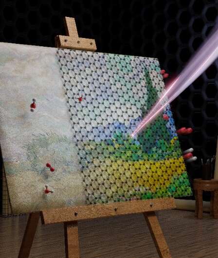
Since its isolation in 2004 by Geim [Andre Geim] and Novoselov [Konstantin Novoselov] from the University of Manchester (Nobel Prize in Physics in 2010), graphene has been termed as a ‘wonder material’ due to its exceptional properties that have already been used in many applications and products. The graphene veil used in this work is a flexible, transparent film, produced by the technique of chemical vapor deposition. It has a monoatomic thickness and, since there are no size limitations in the other dimensions (length and width), it can cover any required large surface areas.

The results from measurements performed in the above mentioned laboratories, showed that this membrane is impermeable to moisture, the oxidizing agents and other harmful pollutants and also can absorb a large amount of harmful ultraviolet radiation. Finally, in contrast to other protective means, it is demonstrated that these graphene coatings are relatively easy to remove without damaging the surface of the artworks.

[downloaded from https://phys.org/news/2021-07-graphene-paving-methods-art.html]

Before getting to the link and citation for the paper, here’s the abstract, which helps fill n a few more details,

Modern and contemporary art materials are generally prone to irreversible colour changes upon exposure to light and oxidizing agents. Graphene can be produced in thin large sheets, blocks ultraviolet light, and is impermeable to oxygen, moisture and corrosive agents; therefore, it has the potential to be used as a transparent layer for the protection of art objects in museums, during storage and transportation. Here we show that a single-layer or multilayer graphene veil, produced by chemical vapour deposition, can be deposited over artworks to protect them efficiently against colour fading, with a protection factor of up to 70%. We also show that this process is reversible since the graphene protective layer can be removed using a soft rubber eraser without causing any damage to the artwork. We have also explored a complementary contactless graphene-based route for colour protection that is based on the deposition of graphene on picture framing glass for use when the directapplication of graphene is not feasible due to surface roughness or artwork fragility. Overall, the present results are a proof of concept of the potential use of graphene as an effective and removable protective advanced material to prevent colour fading in artworks.

And now, a link to and a citation for the paper,

Preventing colour fading in artworks with graphene veils by M. Kotsidi, G. Gorgolis, M. G. Pastore Carbone, G. Anagnostopoulos, G. Paterakis, G. Poggi, A. Manikas, G. Trakakis, P. Baglioni & C. Galiotis. Nature Nanotechnology (2021) DOI: https://doi.org/10.1038/s41565-021-00934-z Published 01 July 2021

This paper is behind a paywall.

Bendable phones that are partially organic

It’s been about nine  or 10 years since I first heard about bendable phones (my September 29, 2010 posting). The concept keeps popping up from time to time (my April 25, 2017 posting) and this time, we have Australian scientists to thank for this latest work described in an October 5, 2018 news item on Nanowerk (Note: A link has been removed),

Engineers at ANU [Australian National University] have invented a semiconductor with organic and inorganic materials that can convert electricity into light very efficiently, and it is thin and flexible enough to help make devices such as mobile phones bendable (Advanced Materials, “Efficient and Layer-Dependent Exciton Pumping across Atomically Thin Organic–Inorganic Type-I Heterostructures”).

The invention also opens the door to a new generation of high-performance electronic devices made with organic materials that will be biodegradable or that can be easily recycled, promising to help substantially reduce e-waste.

An October 5, 2018 ANU press release (also on EurekAlert but published October 4, 2018) expands on the theme,

The huge volumes of e-waste generated by discarded electronic devices around the world is causing irreversible damage to the environment. Australia produces 200,000 tonnes of e-waste every year – only four per cent of this waste is recycled.

The organic component has the thickness of just one atom – made from just carbon and hydrogen – and forms part of the semiconductor that the ANU team developed. The inorganic component has the thickness of around two atoms. The hybrid structure can convert electricity into light efficiently for displays on mobile phones, televisions and other electronic devices.

Lead senior researcher Associate Professor Larry Lu said the invention was a major breakthrough in the field.

“For the first time, we have developed an ultra-thin electronics component with excellent semiconducting properties that is an organic-inorganic hybrid structure and thin and flexible enough for future technologies, such as bendable mobile phones and display screens,” said Associate Professor Lu from the ANU Research School of Engineering.

PhD researcher Ankur Sharma, who recently won the ANU 3-Minute Thesis competition, said experiments demonstrated the performance of their semiconductor would be much more efficient than conventional semiconductors made with inorganic materials such as silicon.

“We have the potential with this semiconductor to make mobile phones as powerful as today’s supercomputers,” said Mr Sharma from the ANU Research School of Engineering.

“The light emission from our semiconducting structure is very sharp, so it can be used for high-resolution displays and, since the materials are ultra-thin, they have the flexibility to be made into bendable screens and mobile phones in the near future.”

The team grew the organic semiconductor component molecule by molecule, in a similar way to 3D printing. The process is called chemical vapour deposition.

“We characterised the opto-electronic and electrical properties of our invention to confirm the tremendous potential of it to be used as a future semiconductor component,” Associate Professor Lu said.

“We are working on growing our semiconductor component on a large scale, so it can be commercialised in collaboration with prospective industry partners.”

Here’s a link to and a citation for the paper,

Efficient and Layer‐Dependent Exciton Pumping across Atomically Thin Organic–Inorganic Type‐I Heterostructures by Linglong Zhang, Ankur Sharma, Yi Zhu, Yuhan Zhang, Bowen Wang, Miheng Dong, Hieu T. Nguyen, Zhu Wang, Bo Wen, Yujie Cao, Boqing Liu, Xueqian Sun, Jiong Yang, Ziyuan Li. Advanced Materials Volume30, Issue 40 1803986 (October 4, 2018) DOI:https://doi.org/10.1002/adma.201803986 First published [onliine]: 30 August 2018

This paper is behind a paywall.

Making graphene cheaply by using soybeans

One of the issues with new materials is being able to produce them in a commercially viable fashion and it seems that researchers in Australia may have helped  to do that with graphene. From a Feb. 15, 2017 news item on phys.org,

A breakthrough by CSIRO-led [Australia’s Commonwealth Scientific and Industrial Research Organisation] scientists has made the world’s strongest material more commercially viable, thanks to the humble soybean.

From a Feb. 15, (?) 2017 CSIRO press release (also on EurekAlert), which originated the news item, expands on the theme (Note: A link has been removed),

Graphene is a carbon material that is one atom thick.

Its thin composition and high conductivity means it is used in applications ranging from miniaturised electronics to biomedical devices.

These properties also enable thinner wire connections; providing extensive benefits for computers, solar panels, batteries, sensors and other devices.

Until now, the high cost of graphene production has been the major roadblock in its commercialisation.

Previously, graphene was grown in a highly-controlled environment with explosive compressed gases, requiring long hours of operation at high temperatures and extensive vacuum processing.

CSIRO scientists have developed a novel “GraphAir” technology which eliminates the need for such a highly-controlled environment.

The technology grows graphene film in ambient air with a natural precursor, making its production faster and simpler.

“This ambient-air process for graphene fabrication is fast, simple, safe, potentially scalable, and integration-friendly,” CSIRO scientist Dr Zhao Jun Han, co-author of the paper published today in Nature Communications said.

“Our unique technology is expected to reduce the cost of graphene production and improve the uptake in new applications.”

GraphAir transforms soybean oil – a renewable, natural material – into graphene films in a single step.

“Our GraphAir technology results in good and transformable graphene properties, comparable to graphene made by conventional methods,” CSIRO scientist and co-author of the study Dr Dong Han Seo said.

With heat, soybean oil breaks down into a range of carbon building units that are essential for the synthesis of graphene.

The team also transformed other types of renewable and even waste oil, such as those leftover from barbecues or cooking, into graphene films.

“We can now recycle waste oils that would have otherwise been discarded and transform them into something useful,” Dr Seo said.

The potential applications of graphene include water filtration and purification, renewable energy, sensors, personalised healthcare and medicine, to name a few.

Graphene has excellent electronic, mechanical, thermal and optical properties as well.

Its uses range from improving battery performance in energy devices, to cheaper solar panels.

CSIRO are looking to partner with industry to find new uses for graphene.

Researchers from The University of Sydney, University of Technology Sydney and The Queensland University of Technology also contributed to this work.

Here’s a link to and a citation for the paper,

Single-step ambient-air synthesis of graphene from renewable precursors as electrochemical genosensor by Dong Han Seo, Shafique Pineda, Jinghua Fang, Yesim Gozukara, Samuel Yick, Avi Bendavid, Simon Kwai Hung Lam, Adrian T. Murdock, Anthony B. Murphy, Zhao Jun Han, & Kostya (Ken) Ostrikov. Nature Communications 8, Article number: 14217 (2017) doi:10.1038/ncomms14217 Published online: 30 January 2017

This is an open access paper.