Tag Archives: data storage

Nanomushroom sensors

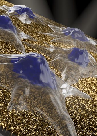
Schematic illustration of cells (blue mountain-like shapes) on top of nanoscale mushroom-like structures with silicone dioxide stems and gold caps, which have the potential to detect cell proliferation in real-time. Courtesy: OIST

The nanomushroom sensors depicted in the above illustration and announced in a February 23, 2018 news item on Nanowerk probably aren’t edible but they certainly make up for that deficiency with other properties,

A small rectangle of pink glass, about the size of a postage stamp, sits on Professor Amy Shen’s desk. Despite its outwardly modest appearance, this little glass slide has the potential to revolutionize a wide range of processes, from monitoring food quality to diagnosing diseases.

The slide is made of a ‘nanoplasmonic’ material — its surface is coated in millions of gold nanostructures, each just a few billionths of a square meter in size. Plasmonic materials absorb and scatter light in interesting ways, giving them unique sensing properties. Nanoplasmonic materials have attracted the attention of biologists, chemists, physicists and material scientists, with possible uses in a diverse array of fields, such as biosensing, data storage, light generation and solar cells.

A February 23, 2018 Okinawa Institute of Science and Technology Graduate University (OIST) press release (also on EurekAlert), which originated the news item, provides more detail,

In several recent papers, Prof. Shen and colleagues at the Micro/Bio/Nanofluidics Unit at the Okinawa Institute of Science and Technology (OIST), described their creation of a new biosensing material that can be used to monitor processes in living cells.

“One of the major goals of nanoplasmonics is to search for better ways to monitor processes in living cells in real time,” says Prof. Shen. Capturing such information can reveal clues about cell behavior, but creating nanomaterials on which cells can survive for long periods of time yet don’t interfere with the cellular processes being measured is a challenge, she explains.

Counting Dividing Cells

One of the team’s new biosensors is made from a nanoplasmonic material that is able to accommodate a large number of cells on a single substrate and to monitor cell proliferation, a fundamental process involving cell growth and division, in real time. Seeing this process in action can reveal important insights into the health and functions of cells and tissues.

Researchers in OIST’s Micro/Bio/Nanofluidics Unit described the sensor in a study recently published in the journal Advanced Biosystems [citation and link follow this press release].

The most attractive feature of the material is that it allows cells to survive over long time periods. “Usually, when you put live cells on a nanomaterial, that material is toxic and it kills the cells,” says Dr. Nikhil Bhalla, a postdoctoral researcher at OIST and first author of the paper. “However, using our material, cells survived for over seven days.” The nanoplasmonic material is also highly sensitive: It can detect an increase in cells as small as 16 in 1000 cells.

The material looks just like an ordinary pieces of glass. However, the surface is coated in tiny nanoplasmonic mushroom-like structures, known as nanomushrooms, with stems of silicon dioxide and caps of gold. Together, these form a biosensor capable of detecting interactions at the molecular level.

The biosensor works by using the nanomushroom caps as optical antennae. When white light passes through the nanoplasmonic slide, the nanomushrooms absorb and scatter some of the light, changing its properties. The absorbance and scattering of light is determined by the size, shape and material of the nanomaterial and, more importantly, it is also affected by any medium in close proximity to the nanomushroom, such as cells that have been placed on the slide. By measuring how the light has changed once it emerges through the other side of the slide, the researchers can detect and monitor processes occurring on the sensor surface, such as cell division.

“Normally, you have to add labels, such as dyes or molecules, to cells, to be able to count dividing cells,” says Dr. Bhalla. “However, with our method, the nanomushrooms can sense them directly.”

Scaling Up

This work builds on a new method, developed by scientists at the Micro/Bio/Nanofluidics Unit at OIST, for fabricating nanomushroom biosensors. The technique was published in the journal ACS Applied Materials and Interfaces in December 2017.

Producing large-scale nanoplasmonic materials is challenging because it is difficult to ensure uniformity across the entire material surface. For this reason, biosensors for routine clinical examinations, such as disease testing, are still lacking.

In response to this problem, the OIST researchers developed a novel printing technique to create large-scale nanomushroom biosensors. With their method, they were able to develop a material consisting of approximately one million mushroom-like structures on a 2.5cm by 7.5cm silicon dioxide substrate.

“Our technique is like taking a stamp, covering it with ink made from biological molecules, and printing onto the nanoplasmonic slide,” says Shivani Sathish, a PhD student at OIST and co-author of the paper. The biological molecules increase the sensitivity of the material, meaning it can sense extremely low concentrations of substances, such as antibodies, and thus potentially detect diseases in their earliest stages.

“Using our method, it is possible to create a highly sensitive biosensor that can detect even single molecules,” says Dr. Bhalla, first author of the paper.

Plasmonic and nanoplasmonic sensors offer important tools for many fields, from electronics to food production to medicine. For example, in December 2017, second year Ph.D student Ainash Garifullina from the Unit developed a new plasmonic material for monitoring the quality of food products during the manufacturing process. The results were published in the journal Analytical Methods.

Prof. Shen and her unit say that, in the future, nanoplasmonic materials may even be integrated with emerging technologies, such as wireless systems in microfluidic devices, allowing users to take readings remotely and thereby minimizing the risk of contamination.

Here’s a link to and a citation for the paper,

Large-Scale Nanophotonic Structures for Long-Term Monitoring of Cell Proliferation by Nikhil Bhalla, Shivani Sathish, Abhishek Sinha, and Amy Q. Shen. Advanced Biosystems Vol. 2 Issue 2 DOI: 10.1002/adbi.201700258 Version of Record online: 19 JAN 2018

© 2018 WILEY-VCH Verlag GmbH & Co. KGaA, Weinheim

This paper is behind a paywall.

Here’s a link to and a citation for the earlier paper,

Probing specific gravity in real-time with graphene oxide plasmonics by Ainash Garifullina, Nikhil Bhalla, and Amy Q. Shen. Anal. Methods 2018, 10, 290-297 DOI: 10.1039/C7AY02423A first published [online] on 06 Dec 2017

This paper is open access provided you have registered for a free account.

3-D integration of nanotechnologies on a single computer chip

By integrating nanomaterials , a new technique for a 3D computer chip capable of handling today’s huge amount of data has been developed. Weirdly, the first two paragraphs of a July 5, 2017 news item on Nanowerk do not convey the main point (Note: A link has been removed),

As embedded intelligence is finding its way into ever more areas of our lives, fields ranging from autonomous driving to personalized medicine are generating huge amounts of data. But just as the flood of data is reaching massive proportions, the ability of computer chips to process it into useful information is stalling.

Now, researchers at Stanford University and MIT have built a new chip to overcome this hurdle. The results are published today in the journal Nature (“Three-dimensional integration of nanotechnologies for computing and data storage on a single chip”), by lead author Max Shulaker, an assistant professor of electrical engineering and computer science at MIT. Shulaker began the work as a PhD student alongside H.-S. Philip Wong and his advisor Subhasish Mitra, professors of electrical engineering and computer science at Stanford. The team also included professors Roger Howe and Krishna Saraswat, also from Stanford.

This image helps to convey the main points,

Instead of relying on silicon-based devices, a new chip uses carbon nanotubes and resistive random-access memory (RRAM) cells. The two are built vertically over one another, making a new, dense 3-D computer architecture with interleaving layers of logic and memory. Courtesy MIT

As I hove been quite impressed with their science writing, it was a bit surprising to find that the Massachusetts Institute of Technology (MIT) had issued this news release (news item) as it didn’t follow the ‘rules’, i.e., cover as many of the journalistic questions (Who, What, Where, When, Why, and, sometimes, How) as possible in the first sentence/paragraph. This is written more in the style of a magazine article and so the details take a while to emerge, from a July 5, 2017 MIT news release, which originated the news item,

Computers today comprise different chips cobbled together. There is a chip for computing and a separate chip for data storage, and the connections between the two are limited. As applications analyze increasingly massive volumes of data, the limited rate at which data can be moved between different chips is creating a critical communication “bottleneck.” And with limited real estate on the chip, there is not enough room to place them side-by-side, even as they have been miniaturized (a phenomenon known as Moore’s Law).

To make matters worse, the underlying devices, transistors made from silicon, are no longer improving at the historic rate that they have for decades.

The new prototype chip is a radical change from today’s chips. It uses multiple nanotechnologies, together with a new computer architecture, to reverse both of these trends.

Instead of relying on silicon-based devices, the chip uses carbon nanotubes, which are sheets of 2-D graphene formed into nanocylinders, and resistive random-access memory (RRAM) cells, a type of nonvolatile memory that operates by changing the resistance of a solid dielectric material. The researchers integrated over 1 million RRAM cells and 2 million carbon nanotube field-effect transistors, making the most complex nanoelectronic system ever made with emerging nanotechnologies.

The RRAM and carbon nanotubes are built vertically over one another, making a new, dense 3-D computer architecture with interleaving layers of logic and memory. By inserting ultradense wires between these layers, this 3-D architecture promises to address the communication bottleneck.

However, such an architecture is not possible with existing silicon-based technology, according to the paper’s lead author, Max Shulaker, who is a core member of MIT’s Microsystems Technology Laboratories. “Circuits today are 2-D, since building conventional silicon transistors involves extremely high temperatures of over 1,000 degrees Celsius,” says Shulaker. “If you then build a second layer of silicon circuits on top, that high temperature will damage the bottom layer of circuits.”

The key in this work is that carbon nanotube circuits and RRAM memory can be fabricated at much lower temperatures, below 200 C. “This means they can be built up in layers without harming the circuits beneath,” Shulaker says.

This provides several simultaneous benefits for future computing systems. “The devices are better: Logic made from carbon nanotubes can be an order of magnitude more energy-efficient compared to today’s logic made from silicon, and similarly, RRAM can be denser, faster, and more energy-efficient compared to DRAM,” Wong says, referring to a conventional memory known as dynamic random-access memory.

“In addition to improved devices, 3-D integration can address another key consideration in systems: the interconnects within and between chips,” Saraswat adds.

“The new 3-D computer architecture provides dense and fine-grained integration of computating and data storage, drastically overcoming the bottleneck from moving data between chips,” Mitra says. “As a result, the chip is able to store massive amounts of data and perform on-chip processing to transform a data deluge into useful information.”

To demonstrate the potential of the technology, the researchers took advantage of the ability of carbon nanotubes to also act as sensors. On the top layer of the chip they placed over 1 million carbon nanotube-based sensors, which they used to detect and classify ambient gases.

Due to the layering of sensing, data storage, and computing, the chip was able to measure each of the sensors in parallel, and then write directly into its memory, generating huge bandwidth, Shulaker says.

Three-dimensional integration is the most promising approach to continue the technology scaling path set forth by Moore’s laws, allowing an increasing number of devices to be integrated per unit volume, according to Jan Rabaey, a professor of electrical engineering and computer science at the University of California at Berkeley, who was not involved in the research.

“It leads to a fundamentally different perspective on computing architectures, enabling an intimate interweaving of memory and logic,” Rabaey says. “These structures may be particularly suited for alternative learning-based computational paradigms such as brain-inspired systems and deep neural nets, and the approach presented by the authors is definitely a great first step in that direction.”

“One big advantage of our demonstration is that it is compatible with today’s silicon infrastructure, both in terms of fabrication and design,” says Howe.

“The fact that this strategy is both CMOS [complementary metal-oxide-semiconductor] compatible and viable for a variety of applications suggests that it is a significant step in the continued advancement of Moore’s Law,” says Ken Hansen, president and CEO of the Semiconductor Research Corporation, which supported the research. “To sustain the promise of Moore’s Law economics, innovative heterogeneous approaches are required as dimensional scaling is no longer sufficient. This pioneering work embodies that philosophy.”

The team is working to improve the underlying nanotechnologies, while exploring the new 3-D computer architecture. For Shulaker, the next step is working with Massachusetts-based semiconductor company Analog Devices to develop new versions of the system that take advantage of its ability to carry out sensing and data processing on the same chip.

So, for example, the devices could be used to detect signs of disease by sensing particular compounds in a patient’s breath, says Shulaker.

“The technology could not only improve traditional computing, but it also opens up a whole new range of applications that we can target,” he says. “My students are now investigating how we can produce chips that do more than just computing.”

“This demonstration of the 3-D integration of sensors, memory, and logic is an exceptionally innovative development that leverages current CMOS technology with the new capabilities of carbon nanotube field–effect transistors,” says Sam Fuller, CTO emeritus of Analog Devices, who was not involved in the research. “This has the potential to be the platform for many revolutionary applications in the future.”

This work was funded by the Defense Advanced Research Projects Agency [DARPA], the National Science Foundation, Semiconductor Research Corporation, STARnet SONIC, and member companies of the Stanford SystemX Alliance.

Here’s a link to and a citation for the paper,

Three-dimensional integration of nanotechnologies for computing and data storage on a single chip by Max M. Shulaker, Gage Hills, Rebecca S. Park, Roger T. Howe, Krishna Saraswat, H.-S. Philip Wong, & Subhasish Mitra. Nature 547, 74–78 (06 July 2017) doi:10.1038/nature22994 Published online 05 July 2017

This paper is behind a paywall.

Gamechanging electronics with new ultrafast, flexible, and transparent electronics

There are two news bits about game-changing electronics, one from the UK and the other from the US.

United Kingdom (UK)

An April 3, 2017 news item on Azonano announces the possibility of a future golden age of electronics courtesy of the University of Exeter,

Engineering experts from the University of Exeter have come up with a breakthrough way to create the smallest, quickest, highest-capacity memories for transparent and flexible applications that could lead to a future golden age of electronics.

A March 31, 2017 University of Exeter press release (also on EurekAlert), which originated the news item, expands on the theme (Note: Links have been removed),

Engineering experts from the University of Exeter have developed innovative new memory using a hybrid of graphene oxide and titanium oxide. Their devices are low cost and eco-friendly to produce, are also perfectly suited for use in flexible electronic devices such as ‘bendable’ mobile phone, computer and television screens, and even ‘intelligent’ clothing.

Crucially, these devices may also have the potential to offer a cheaper and more adaptable alternative to ‘flash memory’, which is currently used in many common devices such as memory cards, graphics cards and USB computer drives.

The research team insist that these innovative new devices have the potential to revolutionise not only how data is stored, but also take flexible electronics to a new age in terms of speed, efficiency and power.

Professor David Wright, an Electronic Engineering expert from the University of Exeter and lead author of the paper said: “Using graphene oxide to produce memory devices has been reported before, but they were typically very large, slow, and aimed at the ‘cheap and cheerful’ end of the electronics goods market.

“Our hybrid graphene oxide-titanium oxide memory is, in contrast, just 50 nanometres long and 8 nanometres thick and can be written to and read from in less than five nanoseconds – with one nanometre being one billionth of a metre and one nanosecond a billionth of a second.”

Professor Craciun, a co-author of the work, added: “Being able to improve data storage is the backbone of tomorrow’s knowledge economy, as well as industry on a global scale. Our work offers the opportunity to completely transform graphene-oxide memory technology, and the potential and possibilities it offers.”

Here’s a link to and a citation for the paper,

Multilevel Ultrafast Flexible Nanoscale Nonvolatile Hybrid Graphene Oxide–Titanium Oxide Memories by V. Karthik Nagareddy, Matthew D. Barnes, Federico Zipoli, Khue T. Lai, Arseny M. Alexeev, Monica Felicia Craciun, and C. David Wright. ACS Nano, 2017, 11 (3), pp 3010–3021 DOI: 10.1021/acsnano.6b08668 Publication Date (Web): February 21, 2017

Copyright © 2017 American Chemical Society

This paper appears to be open access.

United States (US)

Researchers from Stanford University have developed flexible, biodegradable electronics.

A newly developed flexible, biodegradable semiconductor developed by Stanford engineers shown on a human hair. (Image credit: Bao lab)

A human hair? That’s amazing and this May 3, 2017 news item on Nanowerk reveals more,

As electronics become increasingly pervasive in our lives – from smart phones to wearable sensors – so too does the ever rising amount of electronic waste they create. A United Nations Environment Program report found that almost 50 million tons of electronic waste were thrown out in 2017–more than 20 percent higher than waste in 2015.

Troubled by this mounting waste, Stanford engineer Zhenan Bao and her team are rethinking electronics. “In my group, we have been trying to mimic the function of human skin to think about how to develop future electronic devices,” Bao said. She described how skin is stretchable, self-healable and also biodegradable – an attractive list of characteristics for electronics. “We have achieved the first two [flexible and self-healing], so the biodegradability was something we wanted to tackle.”

The team created a flexible electronic device that can easily degrade just by adding a weak acid like vinegar. The results were published in the Proceedings of the National Academy of Sciences (“Biocompatible and totally disintegrable semiconducting polymer for ultrathin and ultralightweight transient electronics”).

“This is the first example of a semiconductive polymer that can decompose,” said lead author Ting Lei, a postdoctoral fellow working with Bao.

A May 1, 2017 Stanford University news release by Sarah Derouin, which originated the news item, provides more detail,

In addition to the polymer – essentially a flexible, conductive plastic – the team developed a degradable electronic circuit and a new biodegradable substrate material for mounting the electrical components. This substrate supports the electrical components, flexing and molding to rough and smooth surfaces alike. When the electronic device is no longer needed, the whole thing can biodegrade into nontoxic components.

Biodegradable bits

Bao, a professor of chemical engineering and materials science and engineering, had previously created a stretchable electrode modeled on human skin. That material could bend and twist in a way that could allow it to interface with the skin or brain, but it couldn’t degrade. That limited its application for implantable devices and – important to Bao – contributed to waste.

Flexible, biodegradable semiconductor on an avacado

The flexible semiconductor can adhere to smooth or rough surfaces and biodegrade to nontoxic products. (Image credit: Bao lab)

Bao said that creating a robust material that is both a good electrical conductor and biodegradable was a challenge, considering traditional polymer chemistry. “We have been trying to think how we can achieve both great electronic property but also have the biodegradability,” Bao said.

Eventually, the team found that by tweaking the chemical structure of the flexible material it would break apart under mild stressors. “We came up with an idea of making these molecules using a special type of chemical linkage that can retain the ability for the electron to smoothly transport along the molecule,” Bao said. “But also this chemical bond is sensitive to weak acid – even weaker than pure vinegar.” The result was a material that could carry an electronic signal but break down without requiring extreme measures.

In addition to the biodegradable polymer, the team developed a new type of electrical component and a substrate material that attaches to the entire electronic component. Electronic components are usually made of gold. But for this device, the researchers crafted components from iron. Bao noted that iron is a very environmentally friendly product and is nontoxic to humans.

The researchers created the substrate, which carries the electronic circuit and the polymer, from cellulose. Cellulose is the same substance that makes up paper. But unlike paper, the team altered cellulose fibers so the “paper” is transparent and flexible, while still breaking down easily. The thin film substrate allows the electronics to be worn on the skin or even implanted inside the body.

From implants to plants

The combination of a biodegradable conductive polymer and substrate makes the electronic device useful in a plethora of settings – from wearable electronics to large-scale environmental surveys with sensor dusts.

“We envision these soft patches that are very thin and conformable to the skin that can measure blood pressure, glucose value, sweat content,” Bao said. A person could wear a specifically designed patch for a day or week, then download the data. According to Bao, this short-term use of disposable electronics seems a perfect fit for a degradable, flexible design.

And it’s not just for skin surveys: the biodegradable substrate, polymers and iron electrodes make the entire component compatible with insertion into the human body. The polymer breaks down to product concentrations much lower than the published acceptable levels found in drinking water. Although the polymer was found to be biocompatible, Bao said that more studies would need to be done before implants are a regular occurrence.

Biodegradable electronics have the potential to go far beyond collecting heart disease and glucose data. These components could be used in places where surveys cover large areas in remote locations. Lei described a research scenario where biodegradable electronics are dropped by airplane over a forest to survey the landscape. “It’s a very large area and very hard for people to spread the sensors,” he said. “Also, if you spread the sensors, it’s very hard to gather them back. You don’t want to contaminate the environment so we need something that can be decomposed.” Instead of plastic littering the forest floor, the sensors would biodegrade away.

As the number of electronics increase, biodegradability will become more important. Lei is excited by their advancements and wants to keep improving performance of biodegradable electronics. “We currently have computers and cell phones and we generate millions and billions of cell phones, and it’s hard to decompose,” he said. “We hope we can develop some materials that can be decomposed so there is less waste.”

Other authors on the study include Ming Guan, Jia Liu, Hung-Cheng Lin, Raphael Pfattner, Leo Shaw, Allister McGuire, and Jeffrey Tok of Stanford University; Tsung-Ching Huang of Hewlett Packard Enterprise; and Lei-Lai Shao and Kwang-Ting Cheng of University of California, Santa Barbara.

The research was funded by the Air Force Office for Scientific Research; BASF; Marie Curie Cofund; Beatriu de Pinós fellowship; and the Kodak Graduate Fellowship.

Here’s a link to and a citation for the team’s latest paper,

Biocompatible and totally disintegrable semiconducting polymer for ultrathin and ultralightweight transient electronics by Ting Lei, Ming Guan, Jia Liu, Hung-Cheng Lin, Raphael Pfattner, Leo Shaw, Allister F. McGuire, Tsung-Ching Huang, Leilai Shao, Kwang-Ting Cheng, Jeffrey B.-H. Tok, and Zhenan Bao. PNAS 2017 doi: 10.1073/pnas.1701478114 published ahead of print May 1, 2017

This paper is behind a paywall.

The mention of cellulose in the second item piqued my interest so I checked to see if they’d used nanocellulose. No, they did not. Microcrystalline cellulose powder was used to constitute a cellulose film but they found a way to render this film at the nanoscale. From the Stanford paper (Note: Links have been removed),

… Moreover, cellulose films have been previously used as biodegradable substrates in electronics (28⇓–30). However, these cellulose films are typically made with thicknesses well over 10 μm and thus cannot be used to fabricate ultrathin electronics with substrate thicknesses below 1–2 μm (7, 18, 19). To the best of our knowledge, there have been no reports on ultrathin (1–2 μm) biodegradable substrates for electronics. Thus, to realize them, we subsequently developed a method described herein to obtain ultrathin (800 nm) cellulose films (Fig. 1B and SI Appendix, Fig. S8). First, microcrystalline cellulose powders were dissolved in LiCl/N,N-dimethylacetamide (DMAc) and reacted with hexamethyldisilazane (HMDS) (31, 32), providing trimethylsilyl-functionalized cellulose (TMSC) (Fig. 1B). To fabricate films or devices, TMSC in chlorobenzene (CB) (70 mg/mL) was spin-coated on a thin dextran sacrificial layer. The TMSC film was measured to be 1.2 μm. After hydrolyzing the film in 95% acetic acid vapor for 2 h, the trimethylsilyl groups were removed, giving a 400-nm-thick cellulose film. The film thickness significantly decreased to one-third of the original film thickness, largely due to the removal of the bulky trimethylsilyl groups. The hydrolyzed cellulose film is insoluble in most organic solvents, for example, toluene, THF, chloroform, CB, and water. Thus, we can sequentially repeat the above steps to obtain an 800-nm-thick film, which is robust enough for further device fabrication and peel-off. By soaking the device in water, the dextran layer is dissolved, starting from the edges of the device to the center. This process ultimately releases the ultrathin substrate and leaves it floating on water surface (Fig. 3A, Inset).

Finally, I don’t have any grand thoughts; it’s just interesting to see different approaches to flexible electronics.

DNA (deoxyribonucleic acid), music, and data storage

David Bruggeman (Pasco Phronesis blog) has written up, as he so often does, a fascinating art/science piece in his May 28, 2015 post (Note: A link has been removed),

Opening next month [June 2015] at the Dilston Grove Gallery at GDP London is Music of the Spheres, an exhibition that uses bioinformatics to record music.  Dr. Nick Goldman of the European Bioinformatics Institute has been working on new technologies for encoding large amounts of information into DNA.  Collaborating with Charlotte Jarvis, the two have worked on installations of bubbles that would contain DNA encoded with music (the DNA is suspended in soap solution).

There’s more information about the exhibit on the Music of the Spheres webpage on the CGP London website,

Music of the Spheres utilises new bioinformatics technology developed by Dr. Nick Goldman to encode a new musical recording by the Kreutzer Quartet into DNA.

The DNA has been suspended in soap solution and will be used by visual artist Charlotte Jarvis to create performances and installations filled with bubbles. The recording will fill the air, pop on visitors skin and literally bathe the audience in music.

Dr. Nick Goldman and Charlotte Jarvis have been working together for the past year to create a series of moving visual and musical experiences that explore the scope and future ubiquity of DNA technologies.

The Kreutzer Quartet’s new composition for string quartet loosely follows the traditional form of a concerto, in comprising of three musical movements. The second movement only exists in the form of a recording encoded into DNA.

For the exhibition the DNA will be suspended in soap solution and used to create silent installations filled with bubbles. The bubbles will be accompanied by a video projection showing the musicians playing in the server room of the European Bioinformatics Institute, Cambridge.

In response to the growing challenge of storing vast quantities of biological data generated by biomedical research Dr. Nick Goldman and the European Bioinformatics Institute have developed a method to encode huge amounts of information in DNA itself. Every day the huge quantities and speed of data pouring into servers gets larger. When research groups sequence DNA the file sizes are too large to be kept on local computers. It is this problem that was the motivation for Nick Goldman to develop his new technology. Their goal is a system that will safely store the equivalent of one million CDs in a gram of DNA for 10,000 years. Nick’s work was has been featured in The New York Times, The Guardian and on BBC News amongst other media outlets.

The Kreutzer Quartet will play the full-length composition live during the preview on 12 June [2015] timed with the setting of the sun through the large westerly windows. [emphasis mine] During the passage of the second movement the stage will fall silent, the music will be released into the auditorium in the form of bubbles. The performance will be accompanied by film projection and a discussion about the project.

The exhibit runs from June 12 – July 5, 2015. Hours and location can be found on the CGP website.

The Music of the Spheres DNA/music project was first mentioned here in a May 5, 2014 post about the launch of the book ‘Synthetic Aesthetics: Investigating Synthetic Biology’s Designs on Nature’. The launch featured a number of performances and events, scroll down abut 80% of the way for the then description of Music of the Spheres.

Twinkle, Twinkle Little Star (song) could lead to better data storage

A March 16, 2015 news item on Nanowerk features research from the University of Illinois and the song ‘Twinkle, Twinkle Little Star’,

Researchers from the University of Illinois at Urbana-Champaign have demonstrated the first-ever recording of optically encoded audio onto a non-magnetic plasmonic nanostructure, opening the door to multiple uses in informational processing and archival storage.

“The chip’s dimensions are roughly equivalent to the thickness of human hair,” explained Kimani Toussaint, an associate professor of mechanical science and engineering, who led the research.

Specifically, the photographic film property exhibited by an array of novel gold, pillar-supported bowtie nanoantennas (pBNAs)–previously discovered by Toussaint’s group–was exploited to store sound and audio files. Compared with the conventional magnetic film for analog data storage, the storage capacity of pBNAs is around 5,600 times larger, indicating a vast array of potential storage uses.

The researchers have provide a visual image illustrating their work,

Nano piano concept: Arrays of gold, pillar-supported bowtie nanoantennas (bottom left) can be used to record distinct musical notes, as shown in the experimentally obtained dark-field microscopy images (bottom right). These particular notes were used to compose 'Twinkle, Twinkle, Little Star.'  Courtesy of University of Illinois at Urbana-Champaign

Nano piano concept: Arrays of gold, pillar-supported bowtie nanoantennas (bottom left) can be used to record distinct musical notes, as shown in the experimentally obtained dark-field microscopy images (bottom right). These particular notes were used to compose ‘Twinkle, Twinkle, Little Star.’ Courtesy of University of Illinois at Urbana-Champaign

A March 16, 2015 University of Illinois at Urbana-Champaign news release (also on EurekAlert), which originated the news item, describes the research in more detail (Note: Links have been removed),

To demonstrate its abilities to store sound and audio files, the researchers created a musical keyboard or “nano piano,” using the available notes to play the short song, “Twinkle, Twinkle, Little Star.”

“Data storage is one interesting area to think about,” Toussaint said. “For example, one can consider applying this type of nanotechnology to enhancing the niche, but still important, analog technology used in the area of archival storage such as using microfiche. In addition, our work holds potential for on-chip, plasmonic-based information processing.”

The researchers demonstrated that the pBNAs could be used to store sound information either as a temporally varying intensity waveform or a frequency varying intensity waveform. Eight basic musical notes, including middle C, D, and E, were stored on a pBNA chip and then retrieved and played back in a desired order to make a tune.

“A characteristic property of plasmonics is the spectrum,” said Hao Chen, a former postdoctoral researcher in Toussaint’s PROBE laboratory and the first author of the paper, “Plasmon-Assisted Audio Recording,” appearing in the Nature Publishing Group’s Scientific Reports. “Originating from a plasmon-induced thermal effect, well-controlled nanoscale morphological changes allow as much as a 100-nm spectral shift from the nanoantennas. By employing this spectral degree-of-freedom as an amplitude coordinate, the storage capacity can be improved. Moreover, although our audio recording focused on analog data storage, in principle it is still possible to transform to digital data storage by having each bowtie serve as a unit bit 1 or 0. By modifying the size of the bowtie, it’s feasible to further improve the storage capacity.”

The team previously demonstrated that pBNAs experience reduced thermal conduction in comparison to standard bowtie nanoantennas and can easily get hot when irradiated by low-powered laser light. Each bowtie antenna is approximately 250 nm across in dimensions, with each supported on 500-nm tall silicon dioxide posts. A consequence of this is that optical illumination results in subtle melting of the gold, and thus a change in the overall optical response. This shows up as a difference in contrast under white-light illumination.

“Our approach is analogous to the method of ‘optical sound,’ which was developed circa 1920s as part of the effort to make ‘talking’ motion pictures,” the team said in its paper. “Although there were variations of this process, they all shared the same basic principle. An audio pickup, e.g., a microphone, electrically modulates a lamp source. Variations in the intensity of the light source is encoded on semi-transparent photographic film (e.g., as variation in area) as the film is spatially translated. Decoding this information is achieved by illuminating the film with the same light source and picking up the changes in the light transmission on an optical detector, which in turn may be connected to speakers. In the work that we present here, the pBNAs serve the role of the photographic film which we can encode with audio information via direct laser writing in an optical microscope.”

In their approach, the researchers record audio signals by using a microscope to scan a sound-modulated laser beam directly on their nanostructures. Retrieval and subsequent playback is achieved by using the same microscope to image the recorded waveform onto a digital camera, whereby simple signal processing can be performed.

Here’s a link to and a citation for the paper,

Plasmon-Assisted Audio Recording by Hao Chen, Abdul M. Bhuiya, Qing Ding, & Kimani C. Toussaint, Jr. Scientific Reports 5, Article number: 9125 doi:10.1038/srep09125 Published 16 March 2015

This is an open access paper and here is a sample recording courtesy of the researchers and the University of Illinois at Urbana-Champaign,