This research is from Purdue University (Indiana, US) and the University of Virginia (US) increases and improves the interactivity between objects in what’s called the Internet of Things (IoT).
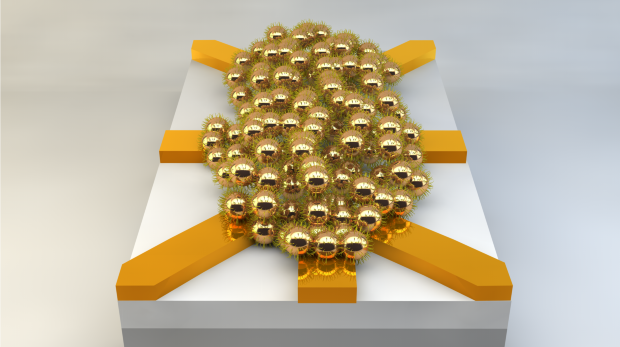
Caption: Electronic stickers can turn ordinary toy blocks into high-tech sensors within the ‘internet of things.’ Credit: Purdue University image/Chi Hwan Lee
From a July 16, 2018 news item on ScienceDaily,
Billions of objects ranging from smartphones and watches to buildings, machine parts and medical devices have become wireless sensors of their environments, expanding a network called the “internet of things.”
As society moves toward connecting all objects to the internet — even furniture and office supplies — the technology that enables these objects to communicate and sense each other will need to scale up.
Researchers at Purdue University and the University of Virginia have developed a new fabrication method that makes tiny, thin-film electronic circuits peelable from a surface. The technique not only eliminates several manufacturing steps and the associated costs, but also allows any object to sense its environment or be controlled through the application of a high-tech sticker.
Eventually, these stickers could also facilitate wireless communication. …
A July 16, 2018 University of Purdue news release (also on EurekAlert), which originated the news item, explains more,
“We could customize a sensor, stick it onto a drone, and send the drone to dangerous areas to detect gas leaks, for example,” said Chi Hwan Lee, Purdue assistant professor of biomedical engineering and mechanical engineering.
Most of today’s electronic circuits are individually built on their own silicon “wafer,” a flat and rigid substrate. The silicon wafer can then withstand the high temperatures and chemical etching that are used to remove the circuits from the wafer.
But high temperatures and etching damage the silicon wafer, forcing the manufacturing process to accommodate an entirely new wafer each time.
Lee’s new fabrication technique, called “transfer printing,” cuts down manufacturing costs by using a single wafer to build a nearly infinite number of thin films holding electronic circuits. Instead of high temperatures and chemicals, the film can peel off at room temperature with the energy-saving help of simply water.
“It’s like the red paint on San Francisco’s Golden Gate Bridge – paint peels because the environment is very wet,” Lee said. “So in our case, submerging the wafer and completed circuit in water significantly reduces the mechanical peeling stress and is environmentally-friendly.”
A ductile metal layer, such as nickel, inserted between the electronic film and the silicon wafer, makes the peeling possible in water. These thin-film electronics can then be trimmed and pasted onto any surface, granting that object electronic features.
Putting one of the stickers on a flower pot, for example, made that flower pot capable of sensing temperature changes that could affect the plant’s growth.
Lee’s lab also demonstrated that the components of electronic integrated circuits work just as well before and after they were made into a thin film peeled from a silicon wafer. The researchers used one film to turn on and off an LED light display.
“We’ve optimized this process so that we can delaminate electronic films from wafers in a defect-free manner,” Lee said.
This technology holds a non-provisional U.S. patent. The work was supported by the Purdue Research Foundation, the Air Force Research Laboratory (AFRL-S-114-054-002), the National Science Foundation (NSF-CMMI-1728149) and the University of Virginia.
The researchers have provided a video,
Here’s a link to and a citation for the paper,
Wafer-recyclable, environment-friendly transfer printing for large-scale thin-film nanoelectronics by Dae Seung Wie, Yue Zhang, Min Ku Kim, Bongjoong Kim, Sangwook Park, Young-Joon Kim, Pedro P. Irazoqui, Xiaolin Zheng, Baoxing Xu, and Chi Hwan Lee.
PNAS July 16, 2018 201806640 DOI: https://doi.org/10.1073/pnas.1806640115
published ahead of print July 16, 2018
This paper is behind a paywall.
Dexter Johnson provides some context in his July 25, 2018 posting on the Nanoclast blog (on the IEEE [Institute of Electronic and Electrical Engineers] website), Note: A link has been removed,
The Internet of Things (IoT), the interconnection of billions of objects and devices that will be communicating with each other, has been the topic of many futurists’ projections. However, getting the engineering sorted out with the aim of fully realizing the myriad visions for IoT is another story. One key issue to address: How do you get the electronics onto these devices efficiently and economically?
A team of researchers from Purdue University and the University of Virginia has developed a new manufacturing process that could make equipping a device with all the sensors and other electronics that will make it Internet capable as easily as putting a piece of tape on it.
…
… this new approach makes use of a water environment at room temperature to control the interfacial debonding process. This allows clean, intact delamination of prefabricated thin film devices when they’re pulled away from the original wafer.
The use of mechanical peeling in water rather than etching solution provides a number of benefits in the manufacturing scheme. Among them are simplicity, controllability, and cost effectiveness, says Chi Hwan Lee, assistant professor at Purdue University and coauthor of the paper chronicling the research.
If you have the time, do read Dexter’s piece. He always adds something that seems obvious in retrospect but wasn’t until he wrote it.