Tag Archives: European Union

Congratulate China on the world’s first quantum communication network

China has some exciting news about the world’s first quantum network; it’s due to open in late August 2017 so you may want to have your congratulations in order for later this month.

An Aug. 4, 2017 news item on phys.org makes the announcement,

As malicious hackers find ever more sophisticated ways to launch attacks, China is about to launch the Jinan Project, the world’s first unhackable computer network, and a major milestone in the development of quantum technology.

Named after the eastern Chinese city where the technology was developed, the network is planned to be fully operational by the end of August 2017. Jinan is the hub of the Beijing-Shanghai quantum network due to its strategic location between the two principal Chinese metropolises.

“We plan to use the network for national defence, finance and other fields, and hope to spread it out as a pilot that if successful can be used across China and the whole world,” commented Zhou Fei, assistant director of the Jinan Institute of Quantum Technology, who was speaking to Britain’s Financial Times.

An Aug. 3, 2017 CORDIS (Community Research and Development Research Information Service [for the European Commission]) press release, which originated the news item, provides more detail about the technology,

By launching the network, China will become the first country worldwide to implement quantum technology for a real life, commercial end. It also highlights that China is a key global player in the rush to develop technologies based on quantum principles, with the EU and the United States also vying for world leadership in the field.

The network, known as a Quantum Key Distribution (QKD) network, is more secure than widely used electronic communication equivalents. Unlike a conventional telephone or internet cable, which can be tapped without the sender or recipient being aware, a QKD network alerts both users to any tampering with the system as soon as it occurs. This is because tampering immediately alters the information being relayed, with the disturbance being instantly recognisable. Once fully implemented, it will make it almost impossible for other governments to listen in on Chinese communications.

In the Jinan network, some 200 users from China’s military, government, finance and electricity sectors will be able to send messages safe in the knowledge that only they are reading them. It will be the world’s longest land-based quantum communications network, stretching over 2 000 km.

Also speaking to the ‘Financial Times’, quantum physicist Tim Byrnes, based at New York University’s (NYU) Shanghai campus commented: ‘China has achieved staggering things with quantum research… It’s amazing how quickly China has gotten on with quantum research projects that would be too expensive to do elsewhere… quantum communication has been taken up by the commercial sector much more in China compared to other countries, which means it is likely to pull ahead of Europe and US in the field of quantum communication.’

However, Europe is also determined to also be at the forefront of the ‘quantum revolution’ which promises to be one of the major defining technological phenomena of the twenty-first century. The EU has invested EUR 550 million into quantum technologies and has provided policy support to researchers through the 2016 Quantum Manifesto.

Moreover, with China’s latest achievement (and a previous one already notched up from July 2017 when its quantum satellite – the world’s first – sent a message to Earth on a quantum communication channel), it looks like the race to be crowned the world’s foremost quantum power is well and truly underway…

Prior to this latest announcement, Chinese scientists had published work about quantum satellite communications, a development that makes their imminent terrestrial quantum network possible. Gabriel Popkin wrote about the quantum satellite in a June 15, 2017 article Science magazine,

Quantum entanglement—physics at its strangest—has moved out of this world and into space. In a study that shows China’s growing mastery of both the quantum world and space science, a team of physicists reports that it sent eerily intertwined quantum particles from a satellite to ground stations separated by 1200 kilometers, smashing the previous world record. The result is a stepping stone to ultrasecure communication networks and, eventually, a space-based quantum internet.

“It’s a huge, major achievement,” says Thomas Jennewein, a physicist at the University of Waterloo in Canada. “They started with this bold idea and managed to do it.”

Entanglement involves putting objects in the peculiar limbo of quantum superposition, in which an object’s quantum properties occupy multiple states at once: like Schrödinger’s cat, dead and alive at the same time. Then those quantum states are shared among multiple objects. Physicists have entangled particles such as electrons and photons, as well as larger objects such as superconducting electric circuits.

Theoretically, even if entangled objects are separated, their precarious quantum states should remain linked until one of them is measured or disturbed. That measurement instantly determines the state of the other object, no matter how far away. The idea is so counterintuitive that Albert Einstein mocked it as “spooky action at a distance.”

Starting in the 1970s, however, physicists began testing the effect over increasing distances. In 2015, the most sophisticated of these tests, which involved measuring entangled electrons 1.3 kilometers apart, showed once again that spooky action is real.

Beyond the fundamental result, such experiments also point to the possibility of hack-proof communications. Long strings of entangled photons, shared between distant locations, can be “quantum keys” that secure communications. Anyone trying to eavesdrop on a quantum-encrypted message would disrupt the shared key, alerting everyone to a compromised channel.

But entangled photons degrade rapidly as they pass through the air or optical fibers. So far, the farthest anyone has sent a quantum key is a few hundred kilometers. “Quantum repeaters” that rebroadcast quantum information could extend a network’s reach, but they aren’t yet mature. Many physicists have dreamed instead of using satellites to send quantum information through the near-vacuum of space. “Once you have satellites distributing your quantum signals throughout the globe, you’ve done it,” says Verónica Fernández Mármol, a physicist at the Spanish National Research Council in Madrid. …

Popkin goes on to detail the process for making the discovery in easily accessible (for the most part) writing and in a video and a graphic.

Russell Brandom writing for The Verge in a June 15, 2017 article about the Chinese quantum satellite adds detail about previous work and teams in other countries also working on the challenge (Note: Links have been removed),

Quantum networking has already shown promise in terrestrial fiber networks, where specialized routing equipment can perform the same trick over conventional fiber-optic cable. The first such network was a DARPA-funded connection established in 2003 between Harvard, Boston University, and a private lab. In the years since, a number of companies have tried to build more ambitious connections. The Swiss company ID Quantique has mapped out a quantum network that would connect many of North America’s largest data centers; in China, a separate team is working on a 2,000-kilometer quantum link between Beijing and Shanghai, which would rely on fiber to span an even greater distance than the satellite link. Still, the nature of fiber places strict limits on how far a single photon can travel.

According to ID Quantique, a reliable satellite link could connect the existing fiber networks into a single globe-spanning quantum network. “This proves the feasibility of quantum communications from space,” ID Quantique CEO Gregoire Ribordy tells The Verge. “The vision is that you have regional quantum key distribution networks over fiber, which can connect to each other through the satellite link.”

China isn’t the only country working on bringing quantum networks to space. A collaboration between the UK’s University of Strathclyde and the National University of Singapore is hoping to produce the same entanglement in cheap, readymade satellites called Cubesats. A Canadian team is also developing a method of producing entangled photons on the ground before sending them into space.

I wonder if there’s going to be an invitational event for scientists around the world to celebrate the launch.
2D printed transistors in Ireland

2D transistors seem to be a hot area for research these days. In Ireland, the AMBER Centre has announced a transistor consisting entirely of 2D nanomaterials in an April 6, 2017 news item on Nanowerk,

Researchers in AMBER, the Science Foundation Ireland-funded materials science research centre hosted in Trinity College Dublin, have fabricated printed transistors consisting entirely of 2-dimensional nanomaterials for the first time. These 2D materials combine exciting electronic properties with the potential for low-cost production.

This breakthrough could unlock the potential for applications such as food packaging that displays a digital countdown to warn you of spoiling, wine labels that alert you when your white wine is at its optimum temperature, or even a window pane that shows the day’s forecast. …

An April 7, 2017 AMBER Centre press release (also on EurekAlert), which originated the news item, expands on the theme,

Prof Jonathan Coleman, who is an investigator in AMBER and Trinity’s School of Physics, said, “In the future, printed devices will be incorporated into even the most mundane objects such as labels, posters and packaging.

Printed electronic circuitry (constructed from the devices we have created) will allow consumer products to gather, process, display and transmit information: for example, milk cartons could send messages to your phone warning that the milk is about to go out-of-date.

We believe that 2D nanomaterials can compete with the materials currently used for printed electronics. Compared to other materials employed in this field, our 2D nanomaterials have the capability to yield more cost effective and higher performance printed devices. However, while the last decade has underlined the potential of 2D materials for a range of electronic applications, only the first steps have been taken to demonstrate their worth in printed electronics. This publication is important because it shows that conducting, semiconducting and insulating 2D nanomaterials can be combined together in complex devices. We felt that it was critically important to focus on printing transistors as they are the electric switches at the heart of modern computing. We believe this work opens the way to print a whole host of devices solely from 2D nanosheets.”

Led by Prof Coleman, in collaboration with the groups of Prof Georg Duesberg (AMBER) and Prof. Laurens Siebbeles (TU Delft,Netherlands), the team used standard printing techniques to combine graphene nanosheets as the electrodes with two other nanomaterials, tungsten diselenide and boron nitride as the channel and separator (two important parts of a transistor) to form an all-printed, all-nanosheet, working transistor.

Printable electronics have developed over the last thirty years based mainly on printable carbon-based molecules. While these molecules can easily be turned into printable inks, such materials are somewhat unstable and have well-known performance limitations. There have been many attempts to surpass these obstacles using alternative materials, such as carbon nanotubes or inorganic nanoparticles, but these materials have also shown limitations in either performance or in manufacturability. While the performance of printed 2D devices cannot yet compare with advanced transistors, the team believe there is a wide scope to improve performance beyond the current state-of-the-art for printed transistors.

The ability to print 2D nanomaterials is based on Prof. Coleman’s scalable method of producing 2D nanomaterials, including graphene, boron nitride, and tungsten diselenide nanosheets, in liquids, a method he has licensed to Samsung and Thomas Swan. These nanosheets are flat nanoparticles that are a few nanometres thick but hundreds of nanometres wide. Critically, nanosheets made from different materials have electronic properties that can be conducting, insulating or semiconducting and so include all the building blocks of electronics. Liquid processing is especially advantageous in that it yields large quantities of high quality 2D materials in a form that is easy to process into inks. Prof. Coleman’s publication provides the potential to print circuitry at extremely low cost which will facilitate a range of applications from animated posters to smart labels.

Prof Coleman is a partner in Graphene flagship, a €1 billion EU initiative to boost new technologies and innovation during the next 10 years.

Here’s a link to and a citation for the paper,

All-printed thin-film transistors from networks of liquid-exfoliated nanosheets by Adam G. Kelly, Toby Hallam, Claudia Backes, Andrew Harvey, Amir Sajad Esmaeily, Ian Godwin, João Coelho, Valeria Nicolosi, Jannika Lauth, Aditya Kulkarni, Sachin Kinge, Laurens D. A. Siebbeles, Georg S. Duesberg, Jonathan N. Coleman. Science  07 Apr 2017: Vol. 356, Issue 6333, pp. 69-73 DOI: 10.1126/science.aal4062

This paper is behind a paywall.

Canada and its Vancouver tech scene gets a boost

Prime Minister Justin Trudeau has been running around attending tech events both in the Vancouver area (Canada) and in Seattle these last few days (May 17 and May 18, 2017). First he attended the Microsoft CEO Summit as noted in a May 11, 2017 news release from the Prime Minister’s Office (Note: I have a few comments about this performance and the Canadian tech scene at the end of this post),

The Prime Minister, Justin Trudeau, today [May 11, 2017] announced that he will participate in the Microsoft CEO Summit in Seattle, Washington, on May 17 and 18 [2017], to promote the Cascadia Innovation Corridor, encourage investment in the Canadian technology sector, and draw global talent to Canada.

This year’s summit, under the theme “The CEO Agenda: Navigating Change,” will bring together more than 150 chief executive officers. While at the Summit, Prime Minister Trudeau will showcase Budget 2017’s Innovation and Skills Plan and demonstrate how Canada is making it easier for Canadian entrepreneurs and innovators to turn their ideas into thriving businesses.

Prime Minister Trudeau will also meet with Washington Governor Jay Inslee.

Quote

“Canada’s greatest strength is its skilled, hard-working, creative, and diverse workforce. Canada is recognized as a world leader in research and development in many areas like artificial intelligence, quantum computing, and 3D programming. Our government will continue to help Canadian businesses grow and create good, well-paying middle class jobs in today’s high-tech economy.”
— Rt. Honourable Justin Trudeau, Prime Minister of Canada

Quick Facts

  • Canada-U.S. bilateral trade in goods and services reached approximately $882 billion in 2016.
  • Nearly 400,000 people and over $2 billion-worth of goods and services cross the Canada-U.S. border every day.
  • Canada-Washington bilateral trade was $19.8 billion in 2016. Some 223,300 jobs in the State of Washington depend on trade and investment with Canada. Canada is among Washington’s top export destinations.

Associated Link

Here’s a little more about the Microsoft meeting from a May 17, 2017 article by Alan Boyle for GeekWire.com (Note: Links have been removed),

So far, this year’s Microsoft CEO Summit has been all about Canadian Prime Minister Justin Trudeau’s talk today, but there’s been precious little information available about who else is attending – and Trudeau may be one of the big reasons why.

Microsoft co-founder Bill Gates created the annual summit back in 1997, to give global business leaders an opportunity to share their experiences and learn about new technologies that will have an impact on business in the future. The event’s attendee list is kept largely confidential, as is the substance of the discussions.

This year, Microsoft says the summit’s two themes are “trust in technology” (as in cybersecurity, international hacking, privacy and the flow of data) and “the race to space” (as in privately funded space efforts such as Amazon billionaire Jeff Bezos’ Blue Origin rocket venture).

Usually, Microsoft lists a few folks who are attending the summit on the company’s Redmond campus, just to give a sense of the event’s cachet. For example, last year’s headliners included Berkshire Hathaway CEO Warren Buffett and Exxon Mobil CEO Rex Tillerson (who is now the Trump administration’s secretary of state)

This year, however, the spotlight has fallen almost exclusively on the hunky 45-year-old Trudeau, the first sitting head of government or state to address the summit. Microsoft isn’t saying anything about the other 140-plus VIPs attending the discussions. “Out of respect for the privacy of our guests, we are not providing any additional information,” a Microsoft spokesperson told GeekWire via email.

Even Trudeau’s remarks at the summit are hush-hush, although officials say he’s talking up Canada’s tech sector.  …

Laura Kane’s May 18, 2017 article for therecord.com provides a little more information about Trudeau’s May 18, 2017 activities in Washington state,

Prime Minister Justin Trudeau continued his efforts to promote Canada’s technology sector to officials in Washington state on Thursday [May 18, 2017], meeting with Gov. Jay Inslee a day after attending the secretive Microsoft CEO Summit.

Trudeau and Inslee discussed, among other issues, the development of the Cascadia Innovation Corridor, an initiative that aims to strengthen technology industry ties between British Columbia and Washington.

The pair also spoke about trade and investment opportunities and innovation in the energy sector, said Trudeau’s office. In brief remarks before the meeting, the prime minister said Washington and Canada share a lot in common.

But protesters clad in yellow hazardous material suits that read “Keystone XL Toxic Cleanup Crew” gathered outside the hotel to criticize Trudeau’s environmental record, arguing his support of pipelines is at odds with any global warming promises he has made.

Later that afternoon, Trudeau visited Electronic Arts (a US games company with offices in the Vancouver area) for more tech talk as Stephanie Ip notes in her May 18, 2017 article for The Vancouver Sun,

Prime Minister Justin Trudeau was in Metro Vancouver Thursday [may 18, 2017] to learn from local tech and business leaders how the federal government can boost B.C.’s tech sector.

The roundtable discussion was organized by the Vancouver Economic Commission and hosted in Burnaby at Electronic Arts’ Capture Lab, where the video game company behind the popular FIFA, Madden and NHL franchises records human movement to add more realism to its digital characters. Representatives from Amazon, Launch Academy, Sony Pictures, Darkhorse 101 Pictures and Front Fundr were also there.

While the roundtable was not open to media, Trudeau met beforehand with media.

“We’re going to talk about how the government can be a better partner or better get out of your way in some cases to allow you to continue to grow, to succeed, to create great opportunities to allow innovation to advance success in Canada and to create good jobs for Canadians and draw in people from around the world and continue to lead the way in the world,” he said.

“Everything from clean tech, to bio-medical advances, to innovation in digital economy — there’s a lot of very, very exciting things going on”

Comments on the US tech sector and the supposed Canadian tech sector

I wonder at all the secrecy. As for the companies mentioned as being at the roundtable, you’ll notice a preponderance of US companies with Launch Academy and Front Fundr (which is not a tech company but a crowdfunding equity company) supplying Canadian content. As for Darkhorse 101 Pictures,  I strongly suspect (after an online search) it is part of Darkhorse Comics (as US company) which has an entertainment division.

Perhaps it didn’t seem worthwhile to mention the Canadian companies? In that case, that’s a sad reflection on how poorly we and our media support our tech sector.

In fact, it seems Trudeau’s version of the Canadian technology sector is for us to continue in our role as a branch plant remaining forever in service of the US economy or at least the US tech sector which may be experiencing some concerns with the US Trump administration and what appears to be an increasingly isolationist perspective with regard to trade and immigration. It’s a perspective that the tech sector, especially the entertainment component, can ill afford.

As for the Cascadia Innovation Corridor mentioned in the Prime Minister’s news release and in Kane’s article, I have more about that in a Feb. 28, 2017 posting about the Cascadia Data Analytics Cooperative.

I noticed he mentioned clean tech as an area of excitement. Well, we just lost a significant player not to the US this time but to the EU (European Union) or more specifically, Germany. (There’ll be more about that in an upcoming post.)

I’m glad to see that Trudeau remains interested in Canadian science and technology but perhaps he could concentrate on new ways of promoting sectoral health rather than relying on the same old thing.

European Commission has issued evaluation of nanomaterial risk frameworks and tools

Despite complaints that there should have been more, there has been some research into risks where nanomaterials are concerned. While additional research would be welcome, it’s perhaps more imperative that standardized testing and risk frameworks are developed so, for example, carbon nanotube safety research in Japan can be compared with the similar research in the Netherlands, the US, and elsewhere. This March 15, 2017 news item on Nanowerk features some research analyzing risk assessment frameworks and tools in Europe,

A recent study has evaluated frameworks and tools used in Europe to assess the potential health and environmental risks of manufactured nanomaterials. The study identifies a trend towards tools that provide protocols for conducting experiments, which enable more flexible and efficient hazard testing. Among its conclusions, however, it notes that no existing frameworks meet all the study’s evaluation criteria and calls for a new, more comprehensive framework.

A March 9, 2017 news alert in the European Commission’s Science for Environment Policy series, which originated the news item, provides more detail (Note: Links have been removed),

Nanotechnology is identified as a key emerging technology in the EU’s growth strategy, Europe 2020. It has great potential to contribute to innovation and economic growth and many of its applications have already received large investments. However,there are some uncertainties surrounding the environmental, health and safety risks of manufactured nanomaterials. For effective regulation, careful scientific analysis of their potential impacts is needed, as conducted through risk assessment exercises.

This study, conducted under the EU-funded MARINA project1, reviewed existing frameworks and tools for risk assessing manufactured nanomaterials. The researchers define a framework as a ‘conceptual paradigm’ of how a risk assessment should be conducted and understood, and give the REACH chemical safety assessment as an example. Tools are defined as implements used to carry out a specific task or function, such as experimental protocols, computer models or databases.

In all, 12 frameworks and 48 tools were evaluated. These were identified from other studies and projects. The frameworks were assessed against eight criteria which represent different strengths, such as whether they consider properties specific to nanomaterials, whether they consider the entire life cycle of a nanomaterial and whether they include careful planning and prioritise objectives before the risk assessment is conducted.

The tools were assessed against seven criteria, such as ease of use, whether they provide quantitative information and if they clearly communicate uncertainty in their results. The researchers defined the criteria for both frameworks and tools by reviewing other studies and by interviewing staff at organisations who develop tools.

The evaluation was thus able to produce a list of strengths and areas for improvement for the frameworks and tools, based on whether they meet each of the criteria. Among its many findings, the evaluation showed that most of the frameworks stress that ‘problem formulation’, which sets the goals and scope of an assessment during the planning process, is essential to avoid unnecessary testing. In addition, most frameworks consider routes of exposure in the initial stages of assessment, which is beneficial as it can exclude irrelevant exposure routes and avoid unnecessary tests.

However, none of the frameworks met all eight of the criteria. The study therefore recommends that a new, comprehensive framework is developed that meets all criteria. Such a framework is needed to inform regulation, the researchers say, and should integrate human health and environmental factors, and cover all stages of the life cycle of a product containing nanomaterials.

The evaluation of the tools suggested that many of them are designed to screen risks, and not necessarily to support regulatory risk assessment. However, their strengths include a growing trend in quantitative models, which can assess uncertainty; for example, one tool analysed can identify uncertainties in its results that are due to gaps in knowledge about a material’s origin, characteristics and use.

The researchers also identified a growing trend in tools that provide protocols for experiments, such as identifying materials and test hazards, which are reproducible across laboratories. These tools could lead to a shift from expensive case-by-case testing for risk assessment of manufactured nanomaterials towards a more efficient process based on groupings of nanomaterials; and ‘read-across’ methods, where the properties of one material can be inferred without testing, based on the known properties of a similar material. The researchers do note, however, that although read-across methods are well established for chemical substances, they are still being developed for nanomaterials. To improve nanomaterial read-across methods, they suggest that more data are needed on the links between nanomaterials’ specific properties and their biological effects.

That’s all, folks.

Graphene-based neural probes

I have two news bits (dated almost one month apart) about the use of graphene in neural probes, one from the European Union and the other from Korea.

European Union (EU)

This work is being announced by the European Commission’s (a subset of the EU) Graphene Flagship (one of two mega-funding projects announced in 2013; 1B Euros each over ten years for the Graphene Flagship and the Human Brain Project).

According to a March 27, 2017 news item on ScienceDaily, researchers have developed a graphene-based neural probe that has been tested on rats,

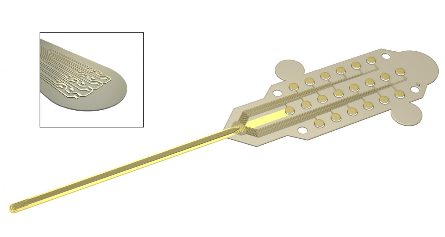
Measuring brain activity with precision is essential to developing further understanding of diseases such as epilepsy and disorders that affect brain function and motor control. Neural probes with high spatial resolution are needed for both recording and stimulating specific functional areas of the brain. Now, researchers from the Graphene Flagship have developed a new device for recording brain activity in high resolution while maintaining excellent signal to noise ratio (SNR). Based on graphene field-effect transistors, the flexible devices open up new possibilities for the development of functional implants and interfaces.

The research, published in 2D Materials, was a collaborative effort involving Flagship partners Technical University of Munich (TU Munich; Germany), Institut d’Investigacions Biomèdiques August Pi i Sunyer (IDIBAPS; Spain), Spanish National Research Council (CSIC; Spain), The Biomedical Research Networking Center in Bioengineering, Biomaterials and Nanomedicine (CIBER-BBN; Spain) and the Catalan Institute of Nanoscience and Nanotechnology (ICN2; Spain).

Caption: Graphene transistors integrated in a flexible neural probe enables electrical signals from neurons to be measured with high accuracy and density. Inset: The tip of the probe contains 16 flexible graphene transistors. Credit: ICN2

A March 27, 2017 Graphene Flagship press release on EurekAlert, which originated the news item, describes the work,  in more detail,

The devices were used to record the large signals generated by pre-epileptic activity in rats, as well as the smaller levels of brain activity during sleep and in response to visual light stimulation. These types of activities lead to much smaller electrical signals, and are at the level of typical brain activity. Neural activity is detected through the highly localised electric fields generated when neurons fire, so densely packed, ultra-small measuring devices is important for accurate brain readings.

The neural probes are placed directly on the surface of the brain, so safety is of paramount importance for the development of graphene-based neural implant devices. Importantly, the researchers determined that the graphene-based probes are non-toxic, and did not induce any significant inflammation.

Devices implanted in the brain as neural prosthesis for therapeutic brain stimulation technologies and interfaces for sensory and motor devices, such as artificial limbs, are an important goal for improving quality of life for patients. This work represents a first step towards the use of graphene in research as well as clinical neural devices, showing that graphene-based technologies can deliver the high resolution and high SNR needed for these applications.

First author Benno Blaschke (TU Munich) said “Graphene is one of the few materials that allows recording in a transistor configuration and simultaneously complies with all other requirements for neural probes such as flexibility, biocompability and chemical stability. Although graphene is ideally suited for flexible electronics, it was a great challenge to transfer our fabrication process from rigid substrates to flexible ones. The next step is to optimize the wafer-scale fabrication process and improve device flexibility and stability.”

Jose Antonio Garrido (ICN2), led the research. He said “Mechanical compliance is an important requirement for safe neural probes and interfaces. Currently, the focus is on ultra-soft materials that can adapt conformally to the brain surface. Graphene neural interfaces have shown already great potential, but we have to improve on the yield and homogeneity of the device production in order to advance towards a real technology. Once we have demonstrated the proof of concept in animal studies, the next goal will be to work towards the first human clinical trial with graphene devices during intraoperative mapping of the brain. This means addressing all regulatory issues associated to medical devices such as safety, biocompatibility, etc.”

Caption: The graphene-based neural probes were used to detect rats’ responses to visual stimulation, as well as neural signals during sleep. Both types of signals are small, and typically difficult to measure. Credit: ICN2

Here’s a link to and a citation for the paper,

Mapping brain activity with flexible graphene micro-transistors by Benno M Blaschke, Núria Tort-Colet, Anton Guimerà-Brunet, Julia Weinert, Lionel Rousseau, Axel Heimann, Simon Drieschner, Oliver Kempski, Rosa Villa, Maria V Sanchez-Vives. 2D Materials, Volume 4, Number 2 DOI https://doi.org/10.1088/2053-1583/aa5eff Published 24 February 2017

© 2017 IOP Publishing Ltd

This paper is behind a paywall.

Korea

While this research from Korea was published more recently, the probe itself has not been subjected to in vivo (animal testing). From an April 19, 2017 news item on ScienceDaily,

Electrodes placed in the brain record neural activity, and can help treat neural diseases like Parkinson’s and epilepsy. Interest is also growing in developing better brain-machine interfaces, in which electrodes can help control prosthetic limbs. Progress in these fields is hindered by limitations in electrodes, which are relatively stiff and can damage soft brain tissue.

Designing smaller, gentler electrodes that still pick up brain signals is a challenge because brain signals are so weak. Typically, the smaller the electrode, the harder it is to detect a signal. However, a team from the Daegu Gyeongbuk Institute of Science & Technology [DGIST} in Korea developed new probes that are small, flexible and read brain signals clearly.

This is a pretty interesting way to illustrate the research,

Caption: Graphene and gold make a better brain probe. Credit: DGIST

An April 19, 2017 DGIST press release (also on EurekAlert), which originated the news item, expands on the theme (Note: A link has been removed),

The probe consists of an electrode, which records the brain signal. The signal travels down an interconnection line to a connector, which transfers the signal to machines measuring and analysing the signals.

The electrode starts with a thin gold base. Attached to the base are tiny zinc oxide nanowires, which are coated in a thin layer of gold, and then a layer of conducting polymer called PEDOT. These combined materials increase the probe’s effective surface area, conducting properties, and strength of the electrode, while still maintaining flexibility and compatibility with soft tissue.

Packing several long, thin nanowires together onto one probe enables the scientists to make a smaller electrode that retains the same effective surface area of a larger, flat electrode. This means the electrode can shrink, but not reduce signal detection. The interconnection line is made of a mix of graphene and gold. Graphene is flexible and gold is an excellent conductor. The researchers tested the probe and found it read rat brain signals very clearly, much better than a standard flat, gold electrode.

“Our graphene and nanowires-based flexible electrode array can be useful for monitoring and recording the functions of the nervous system, or to deliver electrical signals to the brain,” the researchers conclude in their paper recently published in the journal ACS Applied Materials and Interfaces.

The probe requires further clinical tests before widespread commercialization. The researchers are also interested in developing a wireless version to make it more convenient for a variety of applications.

Here’s a link to and a citation for the paper,

Enhancement of Interface Characteristics of Neural Probe Based on Graphene, ZnO Nanowires, and Conducting Polymer PEDOT by Mingyu Ryu, Jae Hoon Yang, Yumi Ahn, Minkyung Sim, Kyung Hwa Lee, Kyungsoo Kim, Taeju Lee, Seung-Jun Yoo, So Yeun Kim, Cheil Moon, Minkyu Je, Ji-Woong Choi, Youngu Lee, and Jae Eun Jang. ACS Appl. Mater. Interfaces, 2017, 9 (12), pp 10577–10586 DOI: 10.1021/acsami.7b02975 Publication Date (Web): March 7, 2017

Copyright © 2017 American Chemical Society

This paper is behind a paywall.

OECD (Organization for Economic Cooperation and Development) Dossiers on Nanomaterials Are of “Little to No Value for assessing risk?”

The announcement that a significant portion of the OECD’s (Organization for Economic Cooperation and Development) dossiers on 11 nanomaterials have next to no value for assessing risk seems a harsh judgment from the Center for International Environmental Law (CIEL). From a March 1, 2017 posting by Lynn L. Bergeson on the Nanotechnology Now,

On February 23, 2017, the Center for International Environmental Law (CIEL) issued a press release announcing a new report, commissioned by CIEL, the European Environmental Citizens’ Organization for Standardization (ECOS), and the Oeko-Institute, that “shows that most of the information made available by the Sponsorship Testing Programme of the Organisation for Economic Co-operation and Development (OECD) is of little to no value for the regulatory risk assessment of nanomaterials.”

Here’s more from the Feb. 23, 3017 CIEL press release, which originated the posting,

The study published today [Feb. 23, 2017] was delivered by the Institute of Occupational Medicine (IOM) based in Singapore. IOM screened the 11,500 pages of raw data of the OECD dossiers on 11 nanomaterials, and analysed all characterisation and toxicity data on three specific nanomaterials – fullerenes, single-walled carbon nanotubes, and zinc oxide.

“EU policy makers and industry are using the existence of the data to dispel concerns about the potential health and environmental risks of manufactured nanomaterials,” said David Azoulay, Senior Attorney for CIEL. “When you analyse the data, in most cases, it is impossible to assess what material was actually tested. The fact that data exists about a nanomaterial does not mean that the information is reliable to assess the hazards or risks of the material.”

The dossiers were published in 2015 by the OECD’s Working Party on Manufactured Nanomaterials (WPMN), which has yet to draw conclusions on the data quality. Despite this missing analysis, some stakeholders participating in EU policy-making – notably the European Chemicals Agency (ECHA) and the European Commission’s Joint Research Centre – have presented the dossiers as containing information on nano-specific human health and environmental impacts. Industry federations and individual companies have taken this a step further emphasizing that there is enough information available to discard most concerns about potential health or environmental risks of manufactured nanomaterials.

“Our study shows these claims that there is sufficient data available on nanomaterials are not only false, but dangerously so,” said Doreen Fedrigo, Senior Policy Officer of ECOS. ”The lack of nano-specific information in the dossiers means that the results of the tests cannot be used as evidence of no ‘nano-effect’ of the tested material. This information is crucial for regulators and producers who need to know the hazard profile of these materials. Analysing the dossiers has shown that legislation detailing nano-specific information requirements is crucial for the regulatory risk assessment of nanomaterials.”

The report provides important recommendations on future steps in the governance of nanomaterials. “Based on our analysis, serious gaps in current dossiers must be filled in with characterisation information, preparation protocols, and exposure data,” said Andreas Hermann of the Oeko-Institute. “Using these dossiers as they are and ignoring these recommendations would mean making decisions on the safety of nanomaterials based on faulty and incomplete data. Our health and environment requires more from producers and regulators.”

CIEL has an Analysis of OECD WPMN Dossiers Regarding the Availability of Data to Evaluate and Regulate Risk (Dec 2016) webpage which provides more information about the dossiers and about the research into the dossiers and includes links to the report, the executive summer, and the dataset,

The Sponsorship Testing Programme of the Working Party on Manufactured Nanomaterials (WPMN) of the Organisation for Economic Co-operation and Development (OECD) started in 2007 with the aim to test a selection of 13 representative nanomaterials for many endpoints. The main objectives of the programme were to better understand what information on intrinsic properties of the nanomaterials might be relevant for exposure and hazards assessment and assess the validity of OECD chemicals Test Guidelines for nanomaterials. The testing programme concluded in 2015 with the publication of dossiers on 11 nanomaterials: 11,500 pages of raw data to be analysed and interpreted.

The WPMN has not drawn conclusions on the data quality, but some stakeholders participating in EU policy-making – notably the European Chemicals Agency and the European Commission’s Joint Research Centre – presented the dossiers as containing much scientific information that provided a better understanding of their nano-specific human health and environmental impacts. Industry federations and individual companies echoed the views, highlighting that there was enough information available to discard most concerns about potential health or environmental risks of manufactured nanomaterials.

As for the OECD, it concluded, even before the publication of the dossiers, that “many of the existing guidelines are also suitable for the safety assessment of nanomaterials” and “the outcomes (of the sponsorship programme) will provide useful information on the ‘intrinsic properties’ of nanomaterials.”

The Center for International Environmental Law (CIEL), the European Citizens’ Organisation for Standardisation (ECOS) and the Öko-Institut commissioned scientific analysis of these dossiers to assess the relevance of the data for regulatory risk assessment.

The resulting report: Analysis of OECD WPMN dossiers regarding the availability of data to evaluate and regulate risk, provides insights illustratating how most of the information made available by the sponsorship programme is of little to no value in identifying hazards or in assessing risks due to nanomaterials.

The analysis shows that:

  • Most studies and documents in the dossiers contain insufficient characterisation data about the specific nanomaterial addressed (size, particle distribution, surface shape, etc.), making it impossible to assess what material was actually tested.
  • This makes it impossible to make any firm statements regarding the nano-specificity of the hazard data published, or the relationship between observed effects and specific nano-scale properties.
  • Less than 2% of the study records provide detail on the size of the nanomaterial tested. Most studies use mass rather than number or size distribution (so not following scientifically recommended reporting practice).
  • The absence of details on the method used to prepare the nanomaterial makes it virtually impossible to correlate an identified hazard with specific nanomaterial characteristic. Since the studies do not indicate dispersion protocols used, it is impossible to assess whether the final dispersion contained the intended mass concentration (or even the actual presence of nanomaterials in the test system), how much agglomeration may have occurred, and how the preparation protocols may have influenced the size distribution.
  • There is not enough nano-specific information in the dossiers to inform about nano-characteristics of the raw material that influence their toxicology. This information is important for regulators and its absence makes information in the dossier irrelevant to develop read-across guidelines.
  • Only about half of the endpoint study records using OECD Test Guideliness (TGs) were delivered using unaltered OECD TGs, thereby respecting the Guidelines’ requirements. The reasons for modifications of the TGs used in the tests are not clear from the documentation. This includes whether the study record was modified to account for challenges related to specific nanomaterial properties or for other, non-nano-specific reasons.
  • The studies do not contain systematic testing of the influence of nano-specific characteristics on the study outcome, and they do not provide the data needed to assess the effect of nano-scale features on the Test Guidelines. Given the absence of fundamental information on nanomaterial characteristics, the dossiers do not provide evidence of the applicability of existing OECD Test Guidelines to nanomaterials.

The analysis therefore dispels several myths created by some stakeholders following publication of the dossiers and provides important perspective for the governance of nanomaterials. In particular, the analysis makes recommendations to:

  • Systematically assess the validity of existing Test Guidelines for relevance to nanomaterials
  • Develop Test Guidelines for dispersion and other test preparations
  • Define the minimum characteristics of nanomaterials that need to be reported
  • Support the build-up of exposure database
  • Fill the gaps in current dossiers with characterisation information, preparation protocols and exposure data

Read full report.
Read executive summary.
Download full dataset.

This is not my area of expertise and while I find the language a bit inflammatory, it’s my understanding that there are great gaps in our understanding of nanomaterials and testing for risk assessment has been criticized for many of the reasons pointed out by CIEL, ECOS, and the Oeko-Institute.

You can find out more about CIEL here; ECOS here; and the Oeko-Institute (also known as Öko-Institute) here.

Drip dry housing

This piece on new construction materials does have a nanotechnology aspect although it’s not made clear exactly how nanotechnology plays a role.

From a Dec. 28, 2016 news item on phys.org (Note: A link has been removed),

The construction industry is preparing to use textiles from the clothing and footwear industries. Gore-Tex-like membranes, which are usually found in weather-proof jackets and trekking shoes, are now being studied to build breathable, water-resistant walls. Tyvek is one such synthetic textile being used as a “raincoat” for homes.

You can find out more about Tyvek here.on the Dupont website.

A Dec. 21, 2016 press release by Chiara Cecchi for Youris ((European Research Media Center), which originated the news item, proceeds with more about textile-type construction materials,

Camping tents, which have been used for ages to protect against wind, ultra-violet rays and rain, have also inspired the modern construction industry, or “buildtech sector”. This new field of research focuses on the different fibres (animal-based such as wool or silk, plant-based such as linen and cotton and synthetic such as polyester and rayon) in order to develop technical or high-performance materials, thus improving the quality of construction, especially for buildings, dams, bridges, tunnels and roads. This is due to the fibres’ mechanical properties, such as lightness, strength, and also resistance to many factors like creep, deterioration by chemicals and pollutants in the air or rain.

“Textiles play an important role in the modernisation of infrastructure and in sustainable buildings”, explains Andrea Bassi, professor at the Department of Civil and Environmental Engineering (DICA), Politecnico of Milan, “Nylon and fiberglass are mixed with traditional fibres to control thermal and acoustic insulation in walls, façades and roofs. Technological innovation in materials, which includes nanotechnologies [emphasis mine] combined with traditional textiles used in clothes, enables buildings and other constructions to be designed using textiles containing steel polyvinyl chloride (PVC) or ethylene tetrafluoroethylene (ETFE). This gives the materials new antibacterial, antifungal and antimycotic properties in addition to being antistatic, sound-absorbing and water-resistant”.

Rooflys is another example. In this case, coated black woven textiles are placed under the roof to protect roof insulation from mould. These building textiles have also been tested for fire resistance, nail sealability, water and vapour impermeability, wind and UV resistance.

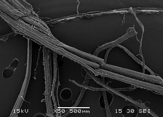
Photo: Production line at the co-operative enterprise CAVAC Biomatériaux, France. Natural fibres processed into a continuous mat (biofib) – Martin Ansell, BRE CICM, University of Bath, UK

In Spain three researchers from the Technical University of Madrid (UPM) have developed a new panel made with textile waste. They claim that it can significantly enhance both the thermal and acoustic conditions of buildings, while reducing greenhouse gas emissions and the energy impact associated with the development of construction materials.

Besides textiles, innovative natural fibre composite materials are a parallel field of the research on insulators that can preserve indoor air quality. These bio-based materials, such as straw and hemp, can reduce the incidence of mould growth because they breathe. The breathability of materials refers to their ability to absorb and desorb moisture naturally”, says expert Finlay White from Modcell, who contributed to the construction of what they claim are the world’s first commercially available straw houses, “For example, highly insulated buildings with poor ventilation can build-up high levels of moisture in the air. If the moisture meets a cool surface it will condensate and producing mould, unless it is managed. Bio-based materials have the means to absorb moisture so that the risk of condensation is reduced, preventing the potential for mould growth”.

The Bristol-based green technology firm [Modcell] is collaborating with the European Isobio project, which is testing bio-based insulators which perform 20% better than conventional materials. “This would lead to a 5% total energy reduction over the lifecycle of a building”, explains Martin Ansell, from BRE Centre for Innovative Construction Materials (BRE CICM), University of Bath, UK, another partner of the project.

“Costs would also be reduced. We are evaluating the thermal and hygroscopic properties of a range of plant-derived by-products including hemp, jute, rape and straw fibres plus corn cob residues. Advanced sol-gel coatings are being deposited on these fibres to optimise these properties in order to produce highly insulating and breathable construction materials”, Ansell concludes.

You can find Modcell here.

Here’s another image, which I believe is a closeup of the processed fibre shown in the above,

Production line at the co-operative enterprise CAVAC Biomatériaux, France. Natural fibres processed into a continuous mat (biofib) – Martin Ansell, BRE CICM, University of Bath, UK [Note: This caption appears to be a copy of the caption for the previous image]

Luminous electronic tiles (lumentile)

A Dec. 19, 2016 news item on Nanowerk introduces a ceramic tile that can be given a different look at the touch of a fingertip,

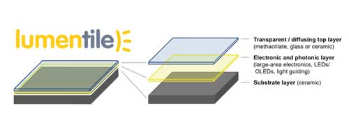
Using pioneering photonics technology, The ‘Luminous Electronic Tile’, or LUMENTILE, project mixes the simplicity of a plain ceramic tile with the complexity of today’s sophisticated touch screen technology, creating a light source and unparalleled interaction. All it takes is one tap to change the colour, look or mood of any room in your house.

This is the first time anyone has tried to embed electronics into ceramics or glass for a large-scale application. With the ability to play videos or display images, the tiles allow the user to turn their walls into a large ‘cinema’ screen, where each unit acts as a set of pixels of the overall display.

An undated Horizon 2020 webpage describes the ‘digital wallpaper’ in more detail,

Scientists from Italy have created ‘digital wallpaper’, allowing for a constant change in design and aesthetic controlled via a smartphone, tablet or computer.

Each Luminous Electronic Tile – or Lumentile – acts as a touch screen which can change colour, pattern or light intensity, play videos or display images.

If numerous tiles are arranged together, they can create a ‘cinema’ screen with each tile acting as a set of pixels for the overall display.

The combination of ceramic, glass and electronics could allow the user to have interchangeable control of the look and design of their surroundings by tapping the tile.

Each tile can be arranged to completely or partially cover walls of a room, floor or ceiling.

However, they can also be transferred to the exterior of buildings, as either flat or curved tiles to fit around columns or uneven surfaces.

Project co-ordinator Professor Guido Giuliani, said: “It may sound like the stuff of James Bond but external tiles would create a ‘chameleonic skin’ or instant camouflage.

“Although we are a long way off this yet, this would allow a car or building to blend completely into its surroundings, and hence ‘disappear’.”

Although these tiles cannot be purchased yet, they hope to be available to users in two years, with mass production by the end of 2020.

Lumentile received a grant of more than €2.4m from the Horizon 2020 programme via the Photonics Public Private Partnership. Created in Italy by the Universita Degli Studi Di Pavia, the Lumentile project also has a number of European partners from Finland, Switzerland and Spain.

A combination of ceramic, glass and organic electronics, the luminous tile includes structural materials, solid-state light sources and electronic chips and can be controlled with a central computer, a smart phone or tablet. [downloaded from http://www.nanowerk.com/nanotechnology-news/newsid=45417.php]

You can find a bit more information on the Lumentile project website.

Graphene Malaysia 2016 gathering and Malaysia’s National Graphene Action Plan 2020

Malaysia is getting ready to host a graphene conference according to an Oct. 10, 2016 news item on Nanotechnology Now,

The Graphene Malaysia 2016 [Nov. 8 – 9, 2016] (www.graphenemalaysiaconf.com) is jointly organized by NanoMalaysia Berhad and Phantoms Foundation. The conference will be centered on graphene industry interaction and collaborative innovation. The event will be launched under the National Graphene Action Plan 2020 (NGAP 2020), which will generate about 9,000 jobs and RM20 (US$4.86) billion GNI impact by the year 2020.

First speakers announced:
Murni Ali (Nanomalaysia, Malaysia) | Francesco Bonaccorso (Istituto Italiano di Tecnologia, Italy) | Antonio Castro Neto (NUS, Singapore) | Antonio Correia (Phantoms Foundation, Spain)| Pedro Gomez-Romero (ICN2 (CSIC-BIST), Spain) | Shu-Jen Han (Nanoscale Science & Technology IBM T.J. Watson Research Center, USA) | Kuan-Tsae Huang (AzTrong, USA/Taiwan) | Krzysztof Koziol (FGV Cambridge Nanosystems, UK) | Taavi Madiberk (Skeleton Technologies, Estonia) | Richard Mckie (BAE Systems, UK) | Pontus Nordin (Saab AB, Saab Aeronautics, Sweden) | Elena Polyakova (Graphene Laboratories Inc., USA) | Ahmad Khairuddin Abdul Rahim (Malaysian Investment Development Authority (MIDA), Malaysia) | Adisorn Tuantranont (Thailand Organic and Printed Electronics Innovation Center, Thailand) |Archana Venugopal (Texas Instruments, USA) | Won Jong Yoo (Samsung-SKKU Graphene-2D Center (SSGC), South Korea) | Hongwei Zhu (Tsinghua University, China)

You can check for more information and deadlines in the Nanotechnology Now Oct. 10, 2016 news item.

The Graphene Malalysia 2016 conference website can be found here and Malaysia’s National Graphene Action Plan 2020, which is well written, can be found here (PDF).  This portion from the executive summary offers some insight into Malyasia’s plans to launch itself into the world of high income nations,

Malaysia’s aspiration to become a high-income nation by 2020 with improved jobs and better outputs is driving the country’s shift away from “business as usual,” and towards more innovative and high value add products. Within this context, and in accordance with National policies and guidelines, Graphene, an emerging, highly versatile carbon-based nanomaterial, presents a unique opportunity for Malaysia to develop a high value economic ecosystem within its industries.  Isolated only in 2004, Graphene’s superior physical properties such as electrical/ thermal conductivity, high strength and high optical transparency, combined with its manufacturability have raised tremendous possibilities for its application across several functions and make it highly interesting for several applications and industries.  Currently, Graphene is still early in its development cycle, affording Malaysian companies time to develop their own applications instead of relying on international intellectual property and licenses.

Considering the potential, several leading countries are investing heavily in associated R&D. Approaches to Graphene research range from an expansive R&D focus (e.g., U.S. and the EU) to more focused approaches aimed at enhancing specific downstream applications with Graphene (e.g., South Korea). Faced with the need to push forward a multitude of development priorities, Malaysia must be targeted in its efforts to capture Graphene’s potential, both in terms of “how to compete” and “where to compete”. This National Graphene Action Plan 2020 lays out a set of priority applications that will be beneficial to the country as a whole and what the government will do to support these efforts.

Globally, much of the Graphene-related commercial innovation to date has been upstream, with producers developing techniques to manufacture Graphene at scale. There has also been some development in downstream sectors, as companies like Samsung, Bayer MaterialScience, BASF and Siemens explore product enhancement with Graphene in lithium-ion battery anodes and flexible displays, and specialty plastic and rubber composites. However the speed of development has been uneven, offering Malaysian industries willing to invest in innovation an opportunity to capture the value at stake. Since any innovation action plan has to be tailored to the needs and ambitions of local industry, Malaysia will focus its Graphene action plan initially on larger domestic industries (e.g., rubber) and areas already being targeted by the government for innovation such as energy storage for electric vehicles and conductive inks.

In addition to benefiting from the physical properties of Graphene, Malaysian downstream application providers may also capture the benefits of a modest input cost advantage for the domestic production of Graphene.  One commonly used Graphene manufacturing technique, the chemical vapour deposition (CVD) production method, requires methane as an input, which can be sourced economically from local biomass. While Graphene is available commercially from various producers around the world, downstream players may be able to enjoy some cost advantage from local Graphene supply. In addition, co-locating with a local producer for joint product development has the added benefit of speeding up the R&D lifecycle.

That business about finding downstream applications could also to the Canadian situation where we typically offer our resources (upstream) but don’t have an active downstream business focus. For example, we have graphite mines in Ontario and Québec which supply graphite flakes for graphene production which is all upstream. Less well developed are any plans for Canadian downstream applications.

Finally, it was interesting to note that the Phantoms Foundation is organizing this Malaysian conference since the same organization is organizing the ‘2nd edition of Graphene & 2D Materials Canada 2016 International Conference & Exhibition’ (you can find out more about the Oct. 18 – 20, 2016 event in my Sept. 23, 2016 posting). I think the Malaysians have a better title for their conference, far less unwieldy.