Tag Archives: Fabio Bergamin

A biochemical means of protecting passwords and anti-counterfeiting solution for art and other precious goods

I guess you could say my passwords are as precious to me as a piece.of art is to some people.

DNA can be used to confirm the authenticity of valuable art prints. (AI-​generated image: ETH Zurich)

An April 8, 2024 ETH Zurich press release (also on EurekAlert) by Fabio Bergamin features an approach that could make passwords secure from quantum computers, Note: A link has been removed,

Security experts fear Q-​Day, the day when quantum computers become so powerful that they can crack today’s passwords. Some experts estimate that this day will come within the next ten years. Password checks are based on cryptographic one-​way functions, which calculate an output value from an input value. This makes it possible to check the validity of a password without transmitting the password itself: the one-​way function converts the password into an output value that can then be used to check its validity in, say, online banking. What makes one-​way functions special is that it’s impossible to use their output value to deduce the input value – in other words, the password. At least not with today’s resources. However, future quantum computers could make this kind of inverse calculation easier.

Researchers at ETH Zurich have now presented a cryptographic one-​way function that works differently from today’s and will also be secure in the future. Rather than processing the data using arithmetic operations, it is stored as a sequence of nucleotides – the chemical building blocks of DNA.

Based on true randomness

“Our system is based on true randomness. The input and output values are physically linked, and it’s only possible to get from the input value to the output value, not the other way round,” explains Robert Grass, a professor in the Department of Chemistry and Applied Biosciences. “Since it’s a physical system and not a digital one, it can’t be decoded by an algorithm, not even by one that runs on a quantum computer,” adds Anne Lüscher, a doctoral student in Grass’s group. She is the lead author of the paper, which was published in the journal Nature Communications.

The researchers’ new system can serve as a counterfeit-​proof way of certifying the authenticity of valuable objects such as works of art. The technology could also be used to trace raw materials and industrial products.

How it works

The new biochemical one-​way function is based on a pool of one hundred million different DNA molecules. Each of the molecules contains two segments featuring a random sequence of nucleotides: one segment for the input value and one for the output value. There are several hundred identical copies of each of these DNA molecules in the pool, and the pool can also be divided into several pools; these are identical because they contain the same random DNA molecules. The pools can be located in different places, or they can be built into objects.

Anyone in possession of this DNA pool holds the security system’s lock. The polymerase chain reaction (PCR) can be used to test a key, or input value, which takes the form of a short sequence of nucleotides. During the PCR, this key searches the pool of hundreds of millions of DNA molecules for the molecule with the matching input value, and the PCR then amplifies the output value located on the same molecule. DNA sequencing is used to make the output value readable.

At first glance, the principle seems complicated. “However, producing DNA molecules with built-​in randomness is cheap and easy,” Grass says. The production costs for a DNA pool that can be divided up in this way are less than 1 Swiss franc. Using DNA sequencing to read out the output value is more time-​consuming and expensive, but many biology laboratories already possess the necessary equipment.

Securing valuable goods and supply chains

ETH Zurich has applied for a patent on this new technology. The researchers now want to optimise and refine it to bring it to market. Because using the method calls for specialised laboratory infrastructure, the scientists think the most likely application for this form of password verification is currently for highly sensitive goods or for access to buildings with restricted access. This technology won’t be an option for the broader public to check passwords until DNA sequencing in particular becomes easier.

A little more thought has already gone into the idea of using the technology for the forgery-​proof certification of works of art. For instance, if there are ten copies of a picture, the artist can mark them all with the DNA pool – perhaps by mixing the DNA into the paint, spraying it onto the picture or applying it to a specific spot.

If several owners later wish to have the authenticity of these artworks confirmed, they can get together, agree on a key (i.e. an input value) and carry out the DNA test. All the copies for which the test produces the same output value will have been proven genuine. The new technology could also be used to link crypto-​assets such as NFTs, which exist only in the digital world, to an object and thus to the physical world.

Furthermore, it would support counterfeit-​proof tracking along supply chains of industrial goods or raw materials. “The aviation industry, for example, has to be able to provide complete proof that it uses only original components. Our technology can guarantee traceability,” Grass says. In addition, the method could be used to label the authenticity of original medicines or cosmetics.

Here’s a link to and a citation for the paper,

Chemical unclonable functions based on operable random DNA pools by Anne M. Luescher, Andreas L. Gimpel, Wendelin J. Stark, Reinhard Heckel & Robert N. Grass. Nature Communications volume 15, Article number: 2955 (2024) DOI: https://doi.org/10.1038/s41467-024-47187-7 Published: 05 April 2024

This paper is open access.

Deriving gold from electronic waste

Caption: The gold nugget obtained from computer motherboards in three parts. The largest of these parts is around five millimetres wide. Credit: (Photograph: ETH Zurich / Alan Kovacevic)

A March 1, 2024 ETH Zurich press release (also on EurekAlert but published February 29, 2024) by Fabio Bergamin describes research into reclaiming gold from electronic waste, Note: A link has been removed.

In brief

  • Protein fibril sponges made by ETH Zurich researchers are hugely effective at recovering gold from electronic waste.
  • From 20 old computer motherboards, the researchers retrieved a 22-​carat gold nugget weighing 450 milligrams.
  • Because the method utilises various waste and industry byproducts, it is not only sustainable but cost effective as well.

Transforming base materials into gold was one of the elusive goals of the alchemists of yore. Now Professor Raffaele Mezzenga from the Department of Health Sciences and Technology at ETH Zurich has accomplished something in that vein. He has not of course transformed another chemical element into gold, as the alchemists sought to do. But he has managed to recover gold from electronic waste using a byproduct of the cheesemaking process.

Electronic waste contains a variety of valuable metals, including copper, cobalt, and even significant amounts of gold. Recovering this gold from disused smartphones and computers is an attractive proposition in view of the rising demand for the precious metal. However, the recovery methods devised to date are energy-​intensive and often require the use of highly toxic chemicals. Now, a group led by ETH Professor Mezzenga has come up with a very efficient, cost-​effective, and above all far more sustainable method: with a sponge made from a protein matrix, the researchers have successfully extracted gold from electronic waste.

Selective gold adsorption

To manufacture the sponge, Mohammad Peydayesh, a senior scientist in Mezzenga’s Group, and his colleagues denatured whey proteins under acidic conditions and high temperatures, so that they aggregated into protein nanofibrils in a gel. The scientists then dried the gel, creating a sponge out of these protein fibrils.

To recover gold in the laboratory experiment, the team salvaged the electronic motherboards from 20 old computer motherboards and extracted the metal parts. They dissolved these parts in an acid bath so as to ionise the metals.

When they placed the protein fibre sponge in the metal ion solution, the gold ions adhered to the protein fibres. Other metal ions can also adhere to the fibres, but gold ions do so much more efficiently. The researchers demonstrated this in their paper, which they have published in the journal Advanced Materials.

As the next step, the researchers heated the sponge. This reduced the gold ions into flakes, which the scientists subsequently melted down into a gold nugget. In this way, they obtained a nugget of around 450 milligrams out of the 20 computer motherboards. The nugget was 91 percent gold (the remainder being copper), which corresponds to 22 carats.

Economically viable

The new technology is commercially viable, as Mezzenga’s calculations show: procurement costs for the source materials added to the energy costs for the entire process are 50 times lower than the value of the gold that can be recovered.

Next, the researchers want to develop the technology to ready it for the market. Although electronic waste is the most promising starting product from which they want to extract gold, there are other possible sources. These include industrial waste from microchip manufacturing or from gold-​plating processes. In addition, the scientists plan to investigate whether they can manufacture the protein fibril sponges out of other protein-​rich byproducts or waste products from the food industry.

“The fact I love the most is that we’re using a food industry byproduct to obtain gold from electronic waste,” Mezzenga says. In a very real sense, he observes, the method transforms two waste products into gold. “You can’t get much more sustainable than that!”

If you have a problem accessing either of the two previously provided links to the press release, you can try this February 29, 2024 news item on ScienceDaily.

Here’s a link to and a citation for the paper,

Gold Recovery from E-Waste by Food-Waste Amyloid Aerogels by Mohammad Peydayesh, Enrico Boschi, Felix Donat, Raffaele Mezzenga. DOI: https://doi.org/10.1002/adma.202310642 First published online: 23 January 2024

This paper is open access.

‘No kiln’ ceramics

Sometimes it’s hard to believe what one reads and this piece about ceramics made without kilns  (for me) fits into that category (from a Feb. 28, 2017 ETH Zurich [English: Swiss Federal Institute of Technology in Zurich] [German: Eidgenössische Technische Hochschule Zürich]) press release (also on EurekAlert) by Fabio Bergamin),

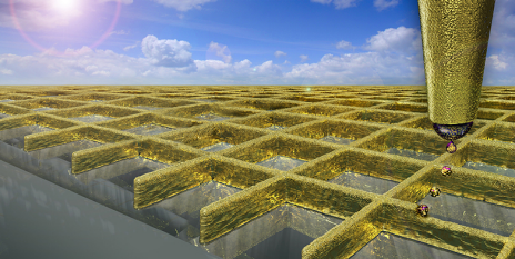
The manufacture of cement, bricks, bathroom tiles and porcelain crockery normally requires a great deal of heat: a kiln is used to fire the ceramic materials at temperatures well in excess of 1,000°C. Now, material scientists from ETH Zurich have developed what seems at first glance to be an astonishingly simple method of manufacture that works at room temperature. The scientists used a calcium carbonate nanopowder as the starting material and instead of firing it, they added a small amount of water and then compacted it.

“The manufacturing process is based on the geological process of rock formation,” explains Florian Bouville, a postdoc in the group of André Studart, Professor of Complex Materials. Sedimentary rock is formed from sediment that is compressed over millions of years through the pressure exerted by overlying deposits. This process turns calcium carbonate sediment into limestone with the help of the surrounding water. As the ETH researchers used calcium carbonate with an extremely fine particle size (nanoparticles) as the starting material, their compacting process took only an hour. “Our work is the first evidence that a piece of ceramic material can be manufactured at room temperature in such a short amount of time and with relatively low pressures,” says ETH professor Studart.

Stronger than concrete

As tests have shown, the new material can withstand about ten times as much force as concrete before it breaks, and is as stiff as stone or concrete. In other words, it is just as hard to deform.

So far, the scientists have produced material samples of about the size of a one-franc piece using a conventional hydraulic press such as those normally used in industry. “The challenge is to generate a sufficiently high pressure for the compacting process. Larger workpieces require a correspondingly greater force,” says Bouville. According to the scientists, ceramic pieces the size of small bathroom tiles should theoretically be feasible.

Energy-efficient and environmentally benign

“For a long time, material scientists have been searching for a way to produce ceramic materials under mild conditions, as the firing process requires a large amount of energy,” says Studart. The new room-temperature method – which experts refer to as cold sintering — is much more energy-efficient and also enables the production of composite materials containing, for example, plastic.

The technique is also of interest with a view to a future CO2-neutral society. Specifically, the carbonate nanoparticles could conceivably be produced using CO2 captured from the atmosphere or from waste gases from thermal power stations. In this scenario, the captured CO2 is allowed to react with a suitable rock in powder form to produce carbonate, which could then be used to manufacture ceramics at room temperature. The climate-damaging CO2 would thus be stored in ceramic products in the long term. These would constitute a CO2 sink and could help thermal power stations to operate on a carbon-neutral basis.

According to the scientists, in the long term, the new approach of cold sintering even has the potential to lead to more environmentally friendly substitutes for cement-based materials. However, great research efforts are needed to reach this goal. Cement production is not only energy-intensive, but it also generates large amounts of CO2 – unlike potential cold-sintered replacement materials.

Here’s a link to and a citation for the paper,

Geologically-inspired strong bulk ceramics made with water at room temperature by Florian Bouville & André R. Studart. Nature Communications 8, Article number: 14655 (2017) doi:10.1038/ncomms14655 Published online: 06 March 2017

This paper is open access.

Florian Bouville’s work in ceramics was last mentioned here in a March 25, 2014 posting.

Nanowalls (like waffles) for touchscreens

ETH Zurich has announced a new technique for creating transparent electrodes in a Jan. 6, 2016 news item on ScienceDaily,

Transparent electrodes have been manufactured for use in touchscreens using a novel nanoprinting process. The new electrodes are some of the most transparent and conductive that have ever been developed.

From smartphones to the operating interfaces of ticket machines and cash dispensers, every touchscreen we use requires transparent electrodes: The devices’ glass surface is coated with a barely visible pattern made of conductive material. It is because of this that the devices recognise whether and where exactly a finger is touching the surface.

Here’s an image illustrating the new electrodes,

With a special mode of electrohydrodynamic ink-jet printing scientists can create a grid of ultra fine gold walls. (Visualisations: Ben Newton / Digit Works)

With a special mode of electrohydrodynamic ink-jet printing scientists can create a grid of ultra fine gold walls. (Visualisations: Ben Newton / Digit Works)

I think these electrodes resemble waffles,

[downloaded from https://github.com/jhermann/Stack-O-Waffles] Credit: jherman

[downloaded from https://github.com/jhermann/Stack-O-Waffles] Credit: jherman

Getting back to the electrodes themselves, a Jan. 6, 2016 ETH Zurich press release (also on EurekAlert*)by Fabio Bergamin, which originated the news item, provides more details,

Researchers under the direction of Dimos Poulikakos, Professor of Thermodynamics, have now used 3D print technology to create a new type of transparent electrode, which takes the form of a grid made of gold or silver “nanowalls” on a glass surface. The walls are so thin that they can hardly be seen with the naked eye. It is the first time that scientists have created nanowalls like these using 3D printing. The new electrodes have a higher conductivity and are more transparent than those made of indium tin oxide, the standard material used in smartphones and tablets today. This is a clear advantage: The more transparent the electrodes, the better the screen quality. And the more conductive they are, the more quickly and precisely the touchscreen will work.

Third dimension

“Indium tin oxide is used because the material has a relatively high degree of transparency and the production of thin layers has been well researched, but it is only moderately conductive,” says Patrik Rohner, a PhD student in Poulikakos’ team. In order to produce more conductive electrodes, the ETH researchers opted for gold and silver, which conduct electricity much better. But because these metals are not transparent, the scientists had to make use of the third dimension. ETH professor Poulikakos explains: “If you want to achieve both high conductivity and transparency in wires made from these metals, you have a conflict of objectives. As the cross-sectional area of gold and silver wires grows, the conductivity increases, but the grid’s transparency decreases.”

The solution was to use metal walls only 80 to 500 nanometres thick, which are almost invisible when viewed from above. Because they are two to four times taller than they are wide, the cross-sectional area, and thus the conductivity, is sufficiently high.

Ink-jet printer with tiny print head

The researchers produced these tiny metal walls using a printing process known as Nanodrip, which Poulikakos and his colleagues developed three years ago. Its basic principle is a process called electrohydrodynamic ink-jet printing. In this process scientists use inks made from metal nanoparticles in a solvent; an electrical field draws ultra-small droplets of the metallic ink out of a glass capillary. The solvent evaporates quickly, allowing a three-dimensional structure to be built up drop by drop.

What is special about the Nanodrip process is that the droplets that come out of the glass capillary are about ten times smaller than the aperture itself. This allows for much smaller structures to be printed. “Imagine a water drop hanging from a tap that is turned off. And now imagine that another tiny droplet is hanging from this drop – we are only printing the tiny droplet,” Poulikakos explains. The researchers managed to create this special form of droplet by perfectly balancing the composition of metallic ink and the electromagnetic field used.

Cost-efficient production

The next big challenge will now be to upscale the method and develop the print process further so that it can be implemented on an industrial scale. To achieve this, the scientists are working with colleagues from ETH spin-off company Scrona.

Here’s a link to and a citation for the paper,

Electrohydrodynamic NanoDrip Printing of High Aspect Ratio Metal Grid Transparent Electrodes by Julian Schneider, Patrick Rohner, Deepankur Thureja, Martin Schmid, Patrick Galliker, Dimos Poulikalos. Advanced Functional Materials DOI: 10.1002/adfm.201503705 First published: 15 December 2015

This paper is behind a paywall.

*'(also on EurekAlert)’ added on Jan. 7, 2016.