Tag Archives: flexible screens

Wearable screen (flexible display) from the University of British Columbia (UBC)

If I read this correctly, the big selling point for UBC’s flexible, wearable display screen is energy efficiency. From a July 10, 2023 University of British Columbia (UBC) news release on EurekAlert,

Imagine a wearable patch that tracks your vital signs through changes in the colour display, or shipping labels that light up to indicate changes in temperature or sterility of food items.

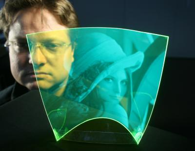
These are among the potential uses for a new flexible display created by UBC researchers and announced recently in ACS Applied Materials and Interfaces.

“This device is capable of fast, realtime and reversible colour change,” says researcher Claire Preston, who developed the device as part of her master’s in electrical and computer engineering at UBC. “It can stretch up to 30 per cent without losing performance. It uses a colour-changing technology that can be used for visual monitoring. And it is relatively cheap to manufacture.”

Previous attempts at creating stretchable displays have involved complex designs and materials, limiting their stretchability and optical quality. In this new research, scientists leaned on electrochromic displays—which are able to reversibly change colour, while requiring low power consumption—to overcome these limitations. [emphasis mine]

“We used PEDOT:PSS, an electrochromic material that consists of a conductive polymer combined with an ionic liquid, resulting in a stretchable electrode that acts as both the electrochromic element and the ion storage layer. This simplifies the device’s architecture and eliminates the need for a separate stretchable conductor,” says Ms. Preston.

The display is transparent and feels like a stiff rubber band. To support the thin layers of PEDOT and allow them to elongate without breaking, the team added a solid polymer electrolyte and a stretchable encapsulation material called styrene-ethylene-butylene-styrene (SEBS).

“The potential uses for this stretchable display are significant. It could be integrated into wearable devices for biometric monitoring, allowing for real-time visual feedback on vital signs. The displays could also be used in robotic skin, enabling robots to display information and interact more intuitively with humans,” noted senior author Dr. John Madden, a professor of electrical and computer engineering who supervised the work.

Additionally, the low power consumption and cost-effectiveness of this technology make it attractive for use in disposable applications such as indicator patches for medical purposes or smart packaging labels for sensitive shipments. It could also be used to actively change the colour of jackets, hats and other garments.

“While there is need for more work to integrate this device into everyday devices, this breakthrough brings us one step closer to a future where flexible and stretchable displays are a common part of our daily lives,” Dr. Madden added.

Here’s a link to and a citation for the paper,

Intrinsically Stretchable Integrated Passive Matrix Electrochromic Display Using PEDOT:PSS Ionic Liquid Composite by Claire Preston, Yuta Dobashi, Ngoc Tan Nguyen, Mirza Saquib Sarwar, Daniel Jun, Cédric Plesse, Xavier Sallenave, Frédéric Vidal, Pierre-Henri Aubert, and John D. W. Madden. ACS Appl. Mater. Interfaces 2023, 15, 23, 28288–28299 DOI: https://doi.org/10.1021/acsami.3c02902 Publication Date: June 5, 2023 Copyright © 2023 The Authors. Published by American Chemical Society

This paper is open access.

Tel Aviv University and the quest for super-slim, bendable displays

It’s beginning to seem like the quest for the Holy Grail. That is, the search for an object more myth than fact, but researchers at Tel Aviv University (TAU) believe they are on the right track to develop a slim, flexible screen according to a March 30, 2015 news item on Nanowerk (Note: A link has been removed),

From smartphones and tablets to computer monitors and interactive TV screens, electronic displays are everywhere. As the demand for instant, constant communication grows, so too does the urgency for more convenient portable devices — especially devices, like computer displays, that can be easily rolled up and put away, rather than requiring a flat surface for storage and transportation.

A new Tel Aviv University study, published recently in Nature Nanotechnology (“Light-emitting self-assembled peptide nucleic acids exhibit both stacking interactions and Watson–Crick base pairing”), suggests that a novel DNA-peptide structure can be used to produce thin, transparent, and flexible screens. The research, conducted by Prof. Ehud Gazit and doctoral student Or Berger of the Department of Molecular Microbiology and Biotechnology at TAU’s Faculty of Life Sciences, in collaboration with Dr. Yuval Ebenstein and Prof. Fernando Patolsky of the School of Chemistry at TAU’s Faculty of Exact Sciences, harnesses bionanotechnology to emit a full range of colors in one pliable pixel layer — as opposed to the several rigid layers that constitute today’s screens.

A March 30, 2015 American Friends of Tel Aviv University news release, which originated the news item, describes the material’s advantages and how the researchers developed it,

“Our material is light, organic, and environmentally friendly,” said Prof. Gazit. “It is flexible, and a single layer emits the same range of light that requires several layers today. By using only one layer, you can minimize production costs dramatically, which will lead to lower prices for consumers as well.”

For the purpose of the study, a part of Berger’s Ph.D. thesis, the researchers tested different combinations of peptides: short protein fragments, embedded with DNA elements which facilitate the self-assembly of a unique molecular architecture.

Peptides and DNA are two of the most basic building blocks of life. Each cell of every life form is composed of such building blocks. In the field of bionanotechnology, scientists utilize these building blocks to develop novel technologies with properties not available for inorganic materials such as plastic and metal.

“Our lab has been working on peptide nanotechnology for over a decade, but DNA nanotechnology is a distinct and fascinating field as well. When I started my doctoral studies, I wanted to try and converge the two approaches,” said Berger. “In this study, we focused on PNA — peptide nucleic acid, a synthetic hybrid molecule of peptides and DNA. We designed and synthesized different PNA sequences, and tried to build nano-metric architectures with them.”

Using methods such as electron microscopy and X-ray crystallography, the researchers discovered that three of the molecules they synthesized could self-assemble, in a few minutes, into ordered structures. The structures resembled the natural double-helix form of DNA, but also exhibited peptide characteristics. This resulted in a very unique molecular arrangement that reflects the duality of the new material.

“Once we discovered the DNA-like organization, we tested the ability of the structures to bind to DNA-specific fluorescent dyes,” said Berger. “To our surprise, the control sample, with no added dye, emitted the same fluorescence as the variable. This proved that the organic structure is itself naturally fluorescent.”

The structures were found to emit light in every color, as opposed to other fluorescent materials that shine only in one specific color. Moreover, light emission was observed also in response to electric voltage — which make it a perfect candidate for opto-electronic devices like display screens.

Here’s a link to and a citation for the paper,

Light-emitting self-assembled peptide nucleic acids exhibit both stacking interactions and Watson–Crick base pairing by Or Berger, Lihi Adler-Abramovich, Michal Levy-Sakin, Assaf Grunwald, Yael Liebes-Peer, Mor Bachar, Ludmila Buzhansky, Estelle Mossou, V. Trevor Forsyth, Tal Schwartz, Yuval Ebenstein, Felix Frolow, Linda J. W. Shimon, Fernando Patolsky, & Ehud Gazit. Nature Nanotechnology (2015) doi:10.1038/nnano.2015.27 Published online 16 March 2015

This paper is behind a paywall but a free preview is available via ReadCube Access.

The age of the ‘nano-pixel’

As mentioned here before, ‘The Diamond Age: Or, A Young Lady’s Illustrated Primer’, a 1985 novel by Neal Stephenson featured in its opening chapter a flexible, bendable, rollable, newspaper screen. It’s one of those devices promised by ‘nano evangelists’ that never quite seems to come into existence. However, ‘hope springs eternally’ as they say and a team from the University of Oxford claims to be bringing us one step closer.

From a July 10, 2014 University of Oxford press release (also on EurekAlert but dated July 9, 2014 and on Azoanano as a July 10, 2014 news item),

A new discovery will make it possible to create pixels just a few hundred nanometres across that could pave the way for extremely high-resolution and low-energy thin, flexible displays for applications such as ‘smart’ glasses, synthetic retinas, and foldable screens.

A team led by Oxford University scientists explored the link between the electrical and optical properties of phase change materials (materials that can change from an amorphous to a crystalline state). They found that by sandwiching a seven nanometre thick layer of a phase change material (GST) between two layers of a transparent electrode they could use a tiny current to ‘draw’ images within the sandwich ‘stack’.

Here’s a series of images the researchers have created using this technology,

Still images drawn with the technology: at around 70 micrometres across each image is smaller than the width of a human hair.  Courtesy University of Oxford

Still images drawn with the technology: at around 70 micrometres across each image is smaller than the width of a human hair. Courtesy University of Oxford

The press release offers a technical description,

Initially still images were created using an atomic force microscope but the team went on to demonstrate that such tiny ‘stacks’ can be turned into prototype pixel-like devices. These ‘nano-pixels’ – just 300 by 300 nanometres in size – can be electrically switched ‘on and off’ at will, creating the coloured dots that would form the building blocks of an extremely high-resolution display technology.

‘We didn’t set out to invent a new kind of display,’ said Professor Harish Bhaskaran of Oxford University’s Department of Materials, who led the research. ‘We were exploring the relationship between the electrical and optical properties of phase change materials and then had the idea of creating this GST ‘sandwich’ made up of layers just a few nanometres thick. We found that not only were we able to create images in the stack but, to our surprise, thinner layers of GST actually gave us better contrast. We also discovered that altering the size of the bottom electrode layer enabled us to change the colour of the image.’

The layers of the GST sandwich are created using a sputtering technique where a target is bombarded with high energy particles so that atoms from the target are deposited onto another material as a thin film.

‘Because the layers that make up our devices can be deposited as thin films they can be incorporated into very thin flexible materials – we have already demonstrated that the technique works on flexible Mylar sheets around 200 nanometres thick,’ said Professor Bhaskaran. ‘This makes them potentially useful for ‘smart’ glasses, foldable screens, windshield displays, and even synthetic retinas that mimic the abilities of photoreceptor cells in the human eye.’

Peiman Hosseini of Oxford University’s Department of Materials, first author of the paper, said: ‘Our models are so good at predicting the experiment that we can tune our prototype ‘pixels’ to create any colour we want – including the primary colours needed for a display. One of the advantages of our design is that, unlike most conventional LCD screens, there would be no need to constantly refresh all pixels, you would only have to refresh those pixels that actually change (static pixels remain as they were). This means that any display based on this technology would have extremely low energy consumption.’

The research suggests that flexible paper-thin displays based on the technology could have the capacity to switch between a power-saving ‘colour e-reader mode’, and a backlit display capable of showing video. Such displays could be created using cheap materials and, because they would be solid-state, promise to be reliable and easy to manufacture. The tiny ‘nano-pixels’ make it ideal for applications, such as smart glasses, where an image would be projected at a larger size as, even enlarged, they would offer very high-resolution.

Professor David Wright of the Department of Engineering at the University of Exeter, co-author of the paper, said: ‘Along with many other researchers around the world we have been looking into the use of these GST materials for memory applications for many years, but no one before thought of combining their electrical and optical functionality to provide entirely new kinds of non-volatile, high-resolution, electronic colour displays – so our work is a real breakthrough.’

The phase change material used was the alloy Ge2Sb2Te5 (Germanium-Antimony-Tellurium or GST) sandwiched between electrode layers made of indium tin oxide (ITO).

I gather the researchers are looking for investors (from the press release),

Whilst the work is still in its early stages, realising its potential, the Oxford team has filed a patent on the discovery with the help of Isis Innovation, Oxford University’s technology commercialisation company. Isis is now discussing the displays with companies who are interested in assessing the technology, and with investors.

Here’s a link to and a citation for the paper,

An optoelectronic framework enabled by low-dimensional phase-change films by Peiman Hosseini, C. David Wright, & Harish Bhaskaran. Nature 511, 206–211 (10 July 2014) doi:10.1038/nature13487 Published online 09 July 2014

This paper is behind a paywall.

Transparent image sensor has no electronics or internal components

This shows the world's first flexible and completely transparent image sensor. The plastic film is coated with fluorescent particles. Credit: Optics Express.

This shows the world’s first flexible and completely transparent image sensor. The plastic film is coated with fluorescent particles. Credit: Optics Express.

Stunning isn’t it? The work is from researchers at the Johannes Kepler University Linz in Austria and is featured in an article being published in Optics Express. From the Feb. 20, 2013 news release about the Optics Express article on EurekAlert,

Digital cameras, medical scanners, and other imaging technologies have advanced considerably during the past decade. Continuing this pace of innovation, an Austrian research team has developed an entirely new way of capturing images based on a flat, flexible, transparent, and potentially disposable polymer sheet. The team describes their new device and its possible applications in a paper published today in the Optical Society’s (OSA) open-access journal Optics Express.

The new imager, which resembles a flexible plastic film, uses fluorescent particles to capture incoming light and channel a portion of it to an array of sensors framing the sheet. With no electronics or internal components, the imager’s elegant design makes it ideal for a new breed of imaging technologies, including user interface devices that can respond not to a touch, but merely to a simple gesture.

The news release goes on to describe the technology,

The sensor is based on a polymer film known as a luminescent concentrator (LC), which is suffused with tiny fluorescent particles that absorb a very specific wavelength (blue light for example) and then reemit it at a longer wavelength (green light for example). Some of the reemitted fluorescent light is scattered out of the imager, but a portion of it travels throughout the interior of the film to the outer edges, where arrays of optical sensors (similar to 1-D pinhole cameras) capture the light. A computer then combines the signals to create a gray-scale image. “With fluorescence, a portion of the light that is reemitted actually stays inside the film,” says Bimber. [Oliver Bimber of the Johannes Kepler University Linz in Austria, co-author of the Optics Express paper] “This is the basic principle of our sensor.”

For the luminescent concentrator to work as an imager, Bimber and his colleagues had to determine precisely where light was falling across the entire surface of the film. This was the major technical challenge because the polymer sheet cannot be divided into individual pixels like the CCD camera inside a smartphone. Instead, fluorescent light from all points across its surface travels to all the edge sensors. Calculating where each bit of light entered the imager would be like determining where along a subway line a passenger got on after the train reached its final destination and all the passengers exited at once.

The solution came from the phenomenon of light attenuation, or dimming, as it travels through the polymer. The longer it travels, the dimmer it becomes. So by measuring the relative brightness of light reaching the sensor array, it was possible to calculate where the light entered the film. This same principle has already been employed in an input device that tracks the location of a single laser point on a screen.

The researchers were able to scale up this basic principle by measuring how much light arrives from every direction at each position on the image sensor at the film’s edge. They could then reconstruct the image by using a technique similar to X-ray computed tomography, more commonly known as a CT scan.

“In CT technology, it’s impossible to reconstruct an image from a single measurement of X-ray attenuation along one scanning direction alone,” says Bimber. “With a multiple of these measurements taken at different positions and directions, however, this becomes possible. Our system works in the same way, but where CT uses X-rays, our technique uses visible light.”

Currently, the resolution from this image sensor is low (32×32 pixels with the first prototypes). The main reason for this is the limited signal-to-noise ratio of the low-cost photodiodes being used. The researchers are planning better prototypes that cool the photodiodes to achieve a higher signal-to-noise ratio.

By applying advanced sampling techniques, the researchers can already enhance the resolution by reconstructing multiple images at different positions on the film. These positions differ by less than a single pixel (as determined by the final image, not the polymer itself). By having multiple of these slightly different images reconstructed, it’s possible to create a higher resolution image. “This does not require better photodiodes,” notes Bimber, “and does not make the sensor significantly slower. The more images we combine, the higher the final resolution is, up to a certain limit.”

The researchers discuss applications,

The main application the researchers envision for this new technology is in touch-free, transparent user interfaces that could seamlessly overlay a television or other display technology. This would give computer operators or video-game players full gesture control without the need for cameras or other external motion-tracking devices. The polymer sheet could also be wrapped around objects to provide them with sensor capabilities. Since the material is transparent, it’s also possible to use multiple layers that each fluoresce at different wavelengths to capture color images.

The researchers also are considering attaching their new sensor in front of a regular, high-resolution CCD sensor. This would allow recording of two images at the same time at two different exposures. “Combining both would give us a high-resolution image with less overexposed or underexposed regions if scenes with a high dynamic range or contrast are captured,” Bimber speculates. He also notes that the polymer sheet portion of the device is relatively inexpensive and therefore disposable. “I think there are many applications for this sensor that we are not yet aware of,” he concludes.

Here’s a citation and a link,

“Towards a transparent, flexible, scalable and disposable image sensor using thin-film luminescent concentrators,” A. Koppelhuber and O. Bimber, Optics Express, Vol. 21, Issue 4, pp. 4796-4810 (2013) (link: http://www.opticsinfobase.org/oe/abstract.cfm?uri=oe-21-4-4796).

Folding screens at University of Toronto and EPD (electronic paper display) with LG

University of Toronto researchers recently announced a breakthrough with regard to organic light-emitting diodes (OLEDs) and flexible screens. From the March 29, 2012 news item by Allyson Rowley on physorg.com,

Michael Helander and Zhibin Wang, PhD candidates in the Faculty of Applied Science and Engineering, are members of a research team that has developed the world’s most efficient organic light-emitting diodes (OLEDs) on flexible plastic. Good news for manufacturers and consumers alike, the discovery means a less costly, more efficient and environmentally friendly way to build brighter flat-panel displays on a thinner, more durable and flexible surface.

The students had been cleaning sheets of indium tin oxide – a material used in all flat-panel displays – when they noticed that devices built using their cleaned sheets had become much more efficient than expected, using less energy to achieve much higher brightness. After some investigation, they determined that this greater efficiency was the result of molecules of chlorine picked up from their cleaning solvent. With this surprising discovery, the two students engineered a prototype for a new kind of OLED device, which is both simpler in construction and more efficient.

According to Rowley’s University of Toronto March 26, 2012 news release,

Over time, though, OLED devices became more complex – the original two layers of molecules became many layers, which raised manufacturing costs and failure rates.

“Basically, we went back to the original idea – and started again,” said Wang. The team’s findings were published, and in December, Helander and Wang, together with Lu [ Professor Zheng-Hong Lu.who supervises both Helander and Wang] and another U of T grad student, launched OTI Lumionics, a startup that will take the next steps toward commercializing the technology.

While OTI Lumionics is taking its next steps, the company, LG Display based in Korea has announced production of a plastic electronic paper display (EPD). From the March 30, 2012 news item by Nancy Owano on physorg.com,

LG Display has set the production clock ticking for a plastic EPD (electronic paper display) product which in turn is expected to set e-book marketability fast-forward. In an announcement Thursday, Korea-based LG Display, which manufactures thin film transistor liquid crystal display, said it has already started up mass production of EPD for e-books.

Amar Toor’s March 29, 2012 item for engadget features the company’s news release, as well as, this detail,

The plan going forward is to supply the display to ODMs [original design manufacturer] in China, in the hopes of bringing final products to Europe by “the beginning of next month.” [May 2012?]

Apparently, the screen resolution is 1024 x 768 and it has a range of 40 degrees when bent from the centre.

Bending and twisting at Ceatac

CEATEC (Cutting Edge IT [Information Technology] and Electronics Comprehensive Exhibition) Japan, Oct.4-8, 2011 is a large technology fair being held in Chiba, near Tokyo. Some 800 companies are showcasing their latest and greatest according to the Oct. 4, 2011 news item on physorg.com,

Around 600 firms unveiled their innovations at the Combined Exhibition of Advanced Technologies (Ceatec) exhibition in Chiba, near Tokyo, expected to draw 200,000 visitors during its five-day run, organisers said.

The impact of Japan’s March 11 earthquake, tsunami and nuclear disaster gave added resonance to technologies on display, particularly those aimed at improving urban infrastructure and energy efficiency.

State-of-the-art radiation counters and power-saving technologies are in high demand after Japan’s disasters sparked fears over contamination and led to power shortages, requiring cuts to energy consumption this summer.

Japanese telecom giant NTT [Nippon Telegraph and Telephone] DoCoMo showed off a smartphone with changeable sensor-embedded shells that can detect bad breath, vital body signs and even be used to measure background radiation levels.

One item that particularly interested me is a transparent organic film from Murata Manufacturing. From the news item,

Electronics parts maker Murata Manufacturing unveiled devices using a newly developed transparent organic film that can deliver instructions via twisting motions or pressure.

One of its gadgets, a light-powered plate called the Leaf Grip Remote Controller, has no buttons but is instead operated by the user bending and twisting it.

Another application of the film is as a touch panel which responds to left-right and up-down finger swipes but also senses how strongly it is being pressed, unlike conventional touchscreen glass used on smartphones.

“Currently we give commands two-dimensionally on touch panels in smartphones and tablet computers but this invention would give us another dimension — how hard they are pressed,” Murata spokesman Kazuhisa Mashita said.

“This could enable users to scroll screens slowly by touching the screen lightly and move images faster by pressing it harder,” he told AFP [Agence France-Presse] ahead of the exhibition.

Earlier this year when CHI (computer-human interface) 2011 was taking place in Vancouver, Canada, I wrote about Roel Vertegaal and his team’s work on their PaperPhone and bending and twisting gestures (May 12, 2011 posting).

Bending and twisting a flexible screen doesn’t seem all that complicated but when you think about making those gestures meaningful,  i. e., ‘slowing a screen image by pressing more softly’, you realize just how much effort and thought are required for features, that if successful, will not be noticed.

Graphene dreams of the Morph

For anyone who’s not familiar with the Morph, it’s an idea that Nokia and the University of Cambridge’s Nanoscience Centre have been working on for the last few years. Originally announced as a type of flexible phone that you could wrap around your wrist, the Morph is now called a concept.  Here’s an animation illustrating some of the concepts which include flexibility and self-cleaning,

There have been very few announcements of any kind about the Morph or the technology that will support this concept. A few months ago, they did make an announcement about researching graphene as a means of actualizing the concept (noted in my May 6, 2011 posting [scroll down about 1/2 way]).

Interestingly the latest research published  on graphene and the flexible, transparent screens that are necessary to making something like the Morph a reality has come from a lab at Rice University. From the August 1, 2011 news item on Nanowerk,

The lab of Rice chemist James Tour lab has created thin films that could revolutionize touch-screen displays, solar panels and LED lighting. The research was reported in the online edition of ACS Nano (“Rational Design of Hybrid Graphene Films for High-Performance Transparent Electrodes”).

Flexible, see-through video screens may be the “killer app” that finally puts graphene — the highly touted single-atom-thick form of carbon — into the commercial spotlight once and for all, Tour said. Combined with other flexible, transparent electronic components being developed at Rice and elsewhere, the breakthrough could lead to computers that wrap around the wrist and solar cells that wrap around just about anything. [emphasis mine]

The lab’s hybrid graphene film is a strong candidate to replace indium tin oxide (ITO), a commercial product widely used as a transparent, conductive coating. It’s the essential element in virtually all flat-panel displays, including touch screens on smart phones and iPads, and is part of organic light-emitting diodes (OLEDs) and solar cells.

Here’s James Tour and Yu Zhu, the paper’s lead author, explaining how the flexible screen was developed,

There are other flexible screens and competitors to the Morph notably the PaperPhone mentioned in my May 6,2011 posting (scroll down about 2/3 of the way) and in my May 12, 2011 posting featuring an interview with Roel Vertegaal of Queen’s University, Ontario, Canada, about the PaperPhone. (We did not discuss the role that graphene might or might not play in the development of the Paperphone’s screens.)

I wonder what impact this work at Rice will have not only for the Morph and the PaperPhone but on the European Union’s pathfinder research competition (the prize is $1B Euros), mentioned in my June 13, 2011 posting about graphene (scroll down about 1/3 of the way). Graphene is one of the research areas being considered for the prize.

ETA Aug. 5, 2011: Tour’s team just published another paper on graphene, one that proves you can make it from anything containing carbon according the Aug. 4, 2011 news item, One Box of Girl Scout Cookies Worth $15 Billion: Lab Shows Troop How Any Carbon Source Can Become Valuable Graphene, on Science Daily,

The cookie gambit started on a dare when Tour mentioned at a meeting that his lab had produced graphene from table sugar.

“I said we could grow it from any carbon source — for example, a Girl Scout cookie, because Girl Scout Cookies were being served at the time,” Tour recalled. “So one of the people in the room said, ‘Yes, please do it. … Let’s see that happen.'”

Members of Girl Scouts of America Troop 25080 came to Rice’s Smalley Institute for Nanoscale Science and Technology to see the process. Rice graduate students Gedeng Ruan, lead author of the paper, and Zhengzong Sun calculated that at the then-commercial rate for pristine graphene — $250 for a two-inch square — a box of traditional Girl Scout shortbread cookies could turn a $15 billion profit.

Here’s the full reference for this second paper,

Gedeng Ruan, Zhengzong Sun, Zhiwei Peng, James M. Tour. Growth of Graphene from Food, Insects and Waste. ACS Nano, 2011; 110729113834087 DOI: 10.1021/nn202625c

The article is behind a paywall.