Tag Archives: gallium

Flat gallium (gallenene) and nanoelectronics

Another day, another 2D material. A March 9, 2018 news item on ScienceDaily announced the latest thin material from Rice university,

Scientists at Rice University and the Indian Institute of Science, Bangalore, have discovered a method to make atomically flat gallium that shows promise for nanoscale electronics.

The Rice lab of materials scientist Pulickel Ajayan and colleagues in India created two-dimensional gallenene, a thin film of conductive material that is to gallium what graphene is to carbon.

Extracted into a two-dimensional form, the novel material appears to have an affinity for binding with semiconductors like silicon and could make an efficient metal contact in two-dimensional electronic devices, the researchers said.

A March 9, 2018 Rice University news release (also on EurekAlert), which originated the news item, describes the process for creating gallenene,

Gallium is a metal with a low melting point; unlike graphene and many other 2-D structures, it cannot yet be grown with vapor phase deposition methods. Moreover, gallium also has a tendency to oxidize quickly. And while early samples of graphene were removed from graphite with adhesive tape, the bonds between gallium layers are too strong for such a simple approach.

So the Rice team led by co-authors Vidya Kochat, a former postdoctoral researcher at Rice, and Atanu Samanta, a student at the Indian Institute of Science, used heat instead of force.

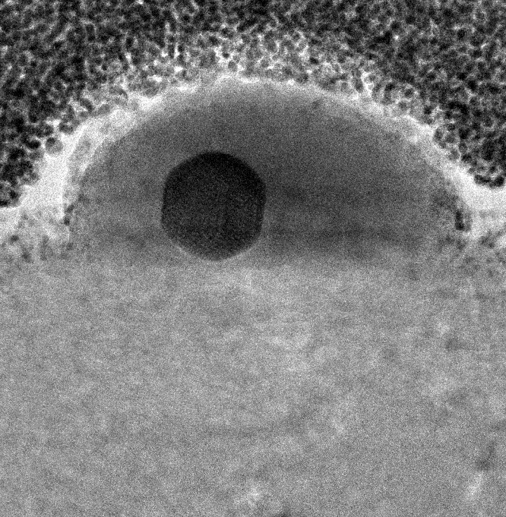
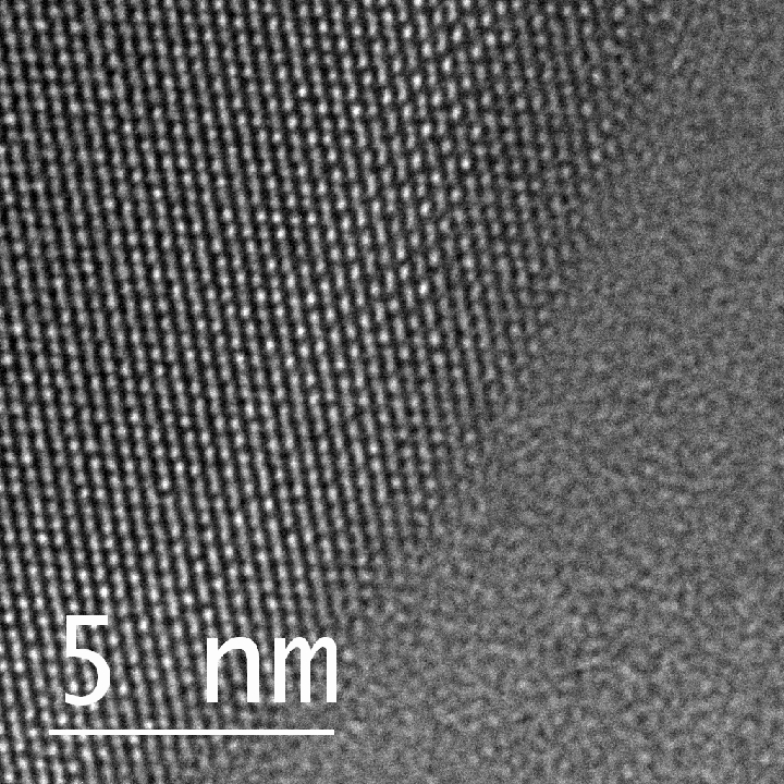
Rather than a bottom-up approach, the researchers worked their way down from bulk gallium by heating it to 29.7 degrees Celsius (about 85 degrees Fahrenheit), just below the element’s melting point. That was enough to drip gallium onto a glass slide. As a drop cooled just a bit, the researchers pressed a flat piece of silicon dioxide on top to lift just a few flat layers of gallenene.

They successfully exfoliated gallenene onto other substrates, including gallium nitride, gallium arsenide, silicone and nickel. That allowed them to confirm that particular gallenene-substrate combinations have different electronic properties and to suggest that these properties can be tuned for applications.

“The current work utilizes the weak interfaces of solids and liquids to separate thin 2-D sheets of gallium,” said Chandra Sekhar Tiwary, principal investigator on the project he completed at Rice before becoming an assistant professor at the Indian Institute of Technology in Gandhinagar, India. “The same method can be explored for other metals and compounds with low melting points.”

Gallenene’s plasmonic and other properties are being investigated, according to Ajayan. “Near 2-D metals are difficult to extract, since these are mostly high-strength, nonlayered structures, so gallenene is an exception that could bridge the need for metals in the 2-D world,” he said.

Co-authors of the paper are graduate student Yuan Zhang and Associate Research Professor Robert Vajtai of Rice; Anthony Stender, a former Rice postdoctoral researcher and now an assistant professor at Ohio University; Sanjit Bhowmick, Praveena Manimunda and Syed Asif of Bruker Nano Surfaces, Minneapolis; and Rice alumnus Abhishek Singh of the Indian Institute of Science. Ajayan is chair of Rice’s Department of Materials Science and NanoEngineering, the Benjamin M. and Mary Greenwood Anderson Professor in Engineering and a professor of chemistry.

The Air Force Office of Scientific Research sponsored the research, with additional support from the Indo-US Science and Technology Forum, the government of India and a Rice Center for Quantum Materials/Smalley-Curl Postdoctoral Fellowship in Quantum Materials.

Here’s a link to and a citation for the paper,

Atomically thin gallium layers from solid-melt exfoliation by Vidya Kochat, Atanu Samanta, Yuan Zhang, Sanjit Bhowmick, Praveena Manimunda, Syed Asif S. Asif, Anthony S. Stender, Robert Vajtai, Abhishek K. Singh, Chandra S. Tiwary, and Pulickel M. Ajayan. Science Advances 09 Mar 2018: Vol. 4, no. 3, e1701373 DOI: 10.1126/sciadv.1701373

This paper appears to be open access.

Substituting graphene and other carbon materials for scarce metals

A Sept. 19, 2017 news item on Nanowerk announces a new paper from the Chalmers University of Technology (Sweden), the lead institution for the Graphene Flagship (a 1B Euro 10 year European Commission programme), Note: A link has been removed,

Scarce metals are found in a wide range of everyday objects around us. They are complicated to extract, difficult to recycle and so rare that several of them have become “conflict minerals” which can promote conflicts and oppression. A survey at Chalmers University of Technology now shows that there are potential technology-based solutions that can replace many of the metals with carbon nanomaterials, such as graphene (Journal of Cleaner Production, “Carbon nanomaterials as potential substitutes for scarce metals”).

They can be found in your computer, in your mobile phone, in almost all other electronic equipment and in many of the plastics around you. Society is highly dependent on scarce metals, and this dependence has many disadvantages.

A Sept. 19, 2017 Chalmers University of Technology press release by Ulrika Ernstrom,, which originated the news item, provides more detail about the possibilities,

They can be found in your computer, in your mobile phone, in many of the plastics around you and in almost all electronic equipment. Society is highly dependent on scarce metals, and this dependence has many disadvantages.
Scarce metals such as tin, silver, tungsten and indium are both rare and difficult to extract since the workable concentrations are very small. This ensures the metals are highly sought after – and their extraction is a breeding ground for conflicts, such as in the Democratic Republic of the Congo where they fund armed conflicts.
In addition, they are difficult to recycle profitably since they are often present in small quantities in various components such as electronics.
Rickard Arvidsson and Björn Sandén, researchers in environmental systems analysis at Chalmers University of Technology, have now examined an alternative solution: substituting carbon nanomaterials for the scarce metals. These substances – the best known of which is graphene – are strong materials with good conductivity, like scarce metals.
“Now technology development has allowed us to make greater use of the common element carbon,” says Sandén. “Today there are many new carbon nanomaterials with similar properties to metals. It’s a welcome new track, and it’s important to invest in both the recycling and substitution of scarce metalsfrom now on.”
The Chalmers researchers have studied  the main applications of 14 different metals, and by reviewing patents and scientific literature have investigated the potential for replacing them by carbon nanomaterials. The results provide a unique overview of research and technology development in the field.
According to Arvidsson and Sandén the summary shows that a shift away from the use of scarce metals to carbon nanomaterials is already taking place.
….
“There are potential technology-based solutions for replacing 13 out of the 14 metals by carbon nanomaterials in their most common applications. The technology development is at different stages for different metals and applications, but in some cases such as indium and gallium, the results are very promising,” Arvidsson says.
“This offers hope,” says Sandén. “In the debate on resource constraints, circular economy and society’s handling of materials, the focus has long been on recycling and reuse. Substitution is a potential alternative that has not been explored to the same extent and as the resource issues become more pressing, we now have more tools to work with.”
The research findings were recently published in the Journal of Cleaner Production. Arvidsson and Sandén stress that there are significant potential benefits from reducing the use of scarce metals, and they hope to be able to strengthen the case for more research and development in the field.
“Imagine being able to replace scarce metals with carbon,” Sandén says. “Extracting the carbon from biomass would create a natural cycle.”
“Since carbon is such a common and readily available material, it would also be possible to reduce the conflicts and geopolitical problems associated with these metals,” Arvidsson says.
At the same time they point out that more research is needed in the field in order to deal with any new problems that may arise if the scarce metals are replaced.
“Carbon nanomaterials are only a relatively recent discovery, and so far knowledge is limited about their environmental impact from a life-cycle perspective. But generally there seems to be a potential for a low environmental impact,” Arvidsson says.

FACTS AND MORE INFORMATION

Carbon nanomaterials consist solely or mainly of carbon, and are strong materials with good conductivity. Several scarce metals have similar properties. The metals are found, for example, in cables, thin screens, flame-retardants, corrosion protection and capacitors.
Rickard Arvidsson and Björn Sandén at Chalmers University of Technology have investigated whether the carbon nanomaterials graphene, fullerenes and carbon nanotubes have the potential to replace 14 scarce metals in their main areas of application (see table). They found potential technology-based solutions to replace the metals with carbon nanomaterials for all applications except for gold in jewellery. The metals which we are closest to being able to substitute are indium, gallium, beryllium and silver.

Here’s a link to and a citation for the paper,

Carbon nanomaterials as potential substitutes for scarce metals by Rickard Arvidsson, Björn A. Sandén. Journal of Cleaner Production (0959-6526). Vol. 156 (2017), p. 253-261. DOI: https://doi.org/10.1016/j.jclepro.2017.04.048

This paper appears to be open access.

Revolutionizing electronics with liquid metal technology?

I’m not sure I’d call it the next big advance in electronics, there are too many advances jockeying for that position but this work from Australia and the US is fascinating. From a Feb. 17, 2017 news item on ScienceDaily,

A new technique using liquid metals to create integrated circuits that are just atoms thick could lead to the next big advance for electronics.

The process opens the way for the production of large wafers around 1.5 nanometres in depth (a sheet of paper, by comparison, is 100,000nm thick).

Other techniques have proven unreliable in terms of quality, difficult to scale up and function only at very high temperatures — 550 degrees or more.

A Feb. 17, 2017 RMIT University press release (also on EurekAlert), which originated the news item, expands on the theme (Note: A link has been removed),

Distinguished Professor Kourosh Kalantar-zadeh, from RMIT’s School of Engineering, led the project, which also included colleagues from RMIT and researchers from CSIRO, Monash University, North Carolina State University and the University of California.

He said the electronics industry had hit a barrier.

“The fundamental technology of car engines has not progressed since 1920 and now the same is happening to electronics. Mobile phones and computers are no more powerful than five years ago.

“That is why this new 2D printing technique is so important – creating many layers of incredibly thin electronic chips on the same surface dramatically increases processing power and reduces costs.

“It will allow for the next revolution in electronics.”

Benjamin Carey, a researcher with RMIT and the CSIRO, said creating electronic wafers just atoms thick could overcome the limitations of current chip production.

It could also produce materials that were extremely bendable, paving the way for flexible electronics.

“However, none of the current technologies are able to create homogenous surfaces of atomically thin semiconductors on large surface areas that are useful for the industrial scale fabrication of chips.

“Our solution is to use the metals gallium and indium, which have a low melting point.

“These metals produce an atomically thin layer of oxide on their surface that naturally protects them. It is this thin oxide which we use in our fabrication method.

“By rolling the liquid metal, the oxide layer can be transferred on to an electronic wafer, which is then sulphurised. The surface of the wafer can be pre-treated to form individual transistors.

“We have used this novel method to create transistors and photo-detectors of very high gain and very high fabrication reliability in large scale.”

Here’s a link to and a citation for the paper,

Wafer-scale two-dimensional semiconductors from printed oxide skin of liquid metals by Benjamin J. Carey, Jian Zhen Ou, Rhiannon M. Clark, Kyle J. Berean, Ali Zavabeti, Anthony S. R. Chesman, Salvy P. Russo, Desmond W. M. Lau, Zai-Quan Xu, Qiaoliang Bao, Omid Kevehei, Brant C. Gibson, Michael D. Dickey, Richard B. Kaner, Torben Daeneke, & Kourosh Kalantar-Zadeh. Nature Communications 8, Article number: 14482 (2017) doi:10.1038/ncomms14482
Published online: 17 February 2017

This paper is open access.

Being solid and liquid over a range of 1000 degrees Fahrenheit means it’s perpetual ice

Duke University researchers along with their international collaborators have made an extraordinary observation. From an Aug. 3, 2016 news item on ScienceDaily,

Imagine pouring a glass of ice water and having the ice cubes remain unchanged hours later, even under a broiler’s heat or in the very back corner of the freezer.

That’s fundamentally the surprising discovery recently made by an international group of researchers led by an electrical engineering professor at Duke University in a paper published online in Nature Matter on July 25, 2016. But instead of a refreshing mixture of H2O in a pint glass, the researchers were working with the chemical element gallium on a nanoscopic scale.

This image shows a single gallium nanoparticle sitting on top of a sapphire base. The black sphere in the center reveals the presence of solid gallium within the liquid drop exterior. The sapphire base is important, as it is rigid with a relatively high surface energy. As the nanoparticle and sapphire try to minimize their total energy, this combination of properties drives the formation and coexistence of the two phases. Courtesy: Duke University

This image shows a single gallium nanoparticle sitting on top of a sapphire base. The black sphere in the center reveals the presence of solid gallium within the liquid drop exterior. The sapphire base is important, as it is rigid with a relatively high surface energy. As the nanoparticle and sapphire try to minimize their total energy, this combination of properties drives the formation and coexistence of the two phases. Courtesy: Duke University

An Aug. 3, 2016 Duke University news release (also on EurekAlert), which originated the news item, explains more about gallium and about this new state,

Gallium is a soft, silvery bluish metal at room temperature. Raise the heat to 86 degrees Fahrenheit, however, and it melts. Drop the temperature to subzero levels, and it becomes hard and brittle. But when gallium nanoparticles sit on top of a sapphire surface, they form a solid core surrounded by a liquid outer layer. The discovery marks the first time that this stable phase coexistence phenomenon at the nanoscale has ever been directly observed.

“This odd combination of a liquid and solid state existing together has been predicted theoretically and observed indirectly in other materials in narrow bands of specific temperatures,” said April Brown, the John Cocke Professor of Electrical and Computer Engineering at Duke. “But this finding was very unexpected, especially because of its stability over such a large temperature range.”

The temperature range Brown is referring to covers more than 1,000 degrees Fahrenheit, all the way from -135 to 980 degrees.

“At a fundamental level, this finding reveals the need to reconsider all our presumptions about solid–liquid equilibrium,” wrote Andrés Aguado, professor of theoretical, atomic and optical physics at the University of Valladolid in Spain, in a News and Views piece appearing in the same edition of Nature Matter. “At a more applied level, the results hold much promise for future nanotechnology applications.”

Gallium is an important element in electronics and is used in microwave circuits, high-speed switching circuits and infrared circuits. The discovery of this novel part-solid, part-liquid nanoparticle phase could be useful in ultraviolet sensors, molecular sensing devices and enhanced photodetectors.

Brown hopes this work is just the tip of the iceberg, as she is planning on creating a facility at Duke to investigate what other nanoparticles might have similar unexpected phase qualities.

The research was conducted in conjunction with researchers at the Institute of Nanotechnology-CNR-Italy, the University of Western Australia, the University of Melbourne and Johannes Kepler University Linz.

This is an atomic view of liquid and solid gallium coexisting in a single nanoparticle taken by a transmission electron microscope. The circular shape on the left-hand side shows gallium atoms in an organized, crystalline, solid structure, while the atoms on the right are in liquid form, showing no organized structure at all. Courtesy: Duke University

This is an atomic view of liquid and solid gallium coexisting in a single nanoparticle taken by a transmission electron microscope. The circular shape on the left-hand side shows gallium atoms in an organized, crystalline, solid structure, while the atoms on the right are in liquid form, showing no organized structure at all. Courtesy: Duke University

Here’s a link to and a citation for the paper,

Thermally stable coexistence of liquid and solid phases in gallium nanoparticles by Maria Losurdo, Alexandra Suvorova, Sergey Rubanov, Kurt Hingerl, & April S. Brown.  Nature Materials (2016) doi:10.1038/nmat4705 Published online 25 July 2016

This paper is behind a paywall.