Tag Archives: Graphene Flagship

Canada’s ‘Smart Cities’ will need new technology (5G wireless) and, maybe, graphene

I recently published [March 20, 2018] a piece on ‘smart cities’ both an art/science event in Toronto and a Canadian government initiative without mentioning the necessity of new technology to support all of the grand plans. On that note, it seems the Canadian federal government and two provincial (Québec and Ontario) governments are prepared to invest in one of the necessary ‘new’ technologies, 5G wireless. The Canadian Broadcasting Corporation’s (CBC) Shawn Benjamin reports about Canada’s 5G plans in suitably breathless (even in text only) tones of excitement in a March 19, 2018 article,

The federal, Ontario and Quebec governments say they will spend $200 million to help fund research into 5G wireless technology, the next-generation networks with download speeds 100 times faster than current ones can handle.

The so-called “5G corridor,” known as ENCQOR, will see tech companies such as Ericsson, Ciena Canada, Thales Canada, IBM and CGI kick in another $200 million to develop facilities to get the project up and running.

The idea is to set up a network of linked research facilities and laboratories that these companies — and as many as 1,000 more across Canada — will be able to use to test products and services that run on 5G networks.

Benjamin’s description of 5G is focused on what it will make possible in the future,

If you think things are moving too fast, buckle up, because a new 5G cellular network is just around the corner and it promises to transform our lives by connecting nearly everything to a new, much faster, reliable wireless network.

The first networks won’t be operational for at least a few years, but technology and telecom companies around the world are already planning to spend billions to make sure they aren’t left behind, says Lawrence Surtees, a communications analyst with the research firm IDC.

The new 5G is no tentative baby step toward the future. Rather, as Surtees puts it, “the move from 4G to 5G is a quantum leap.”

In a downtown Toronto soundstage, Alan Smithson recently demonstrated a few virtual reality and augmented reality projects that his company MetaVRse is working on.

The potential for VR and AR technology is endless, he said, in large part for its potential to help hurdle some of the walls we are already seeing with current networks.

Virtual Reality technology on the market today is continually increasing things like frame rates and screen resolutions in a constant quest to make their devices even more lifelike.

… They [current 4G networks] can’t handle the load. But 5G can do so easily, Smithson said, so much so that the current era of bulky augmented reality headsets could be replaced buy a pair of normal looking glasses.

In a 5G world, those internet-connected glasses will automatically recognize everyone you meet, and possibly be able to overlay their name in your field of vision, along with a link to their online profile. …

Benjamin also mentions ‘smart cities’,

In a University of Toronto laboratory, Professor Alberto Leon-Garcia researches connected vehicles and smart power grids. “My passion right now is enabling smart cities — making smart cities a reality — and that means having much more immediate and detailed sense of the environment,” he said.

Faster 5G networks will assist his projects in many ways, by giving planners more, instant data on things like traffic patterns, energy consumption, variou carbon footprints and much more.

Leon-Garcia points to a brightly lit map of Toronto [image embedded in Benjamin’s article] in his office, and explains that every dot of light represents a sensor transmitting real time data.

Currently, the network is hooked up to things like city buses, traffic cameras and the city-owned fleet of shared bicycles. He currently has thousands of data points feeding him info on his map, but in a 5G world, the network will support about a million sensors per square kilometre.

Very exciting but where is all this data going? What computers will be processing the information? Where are these sensors located? Benjamin does not venture into those waters nor does The Economist in a February 13, 2018 article about 5G, the Olympic Games in Pyeonchang, South Korea, but the magazine does note another barrier to 5G implementation,

“FASTER, higher, stronger,” goes the Olympic motto. So it is only appropriate that the next generation of wireless technology, “5G” for short, should get its first showcase at the Winter Olympics  under way in Pyeongchang, South Korea. Once fully developed, it is supposed to offer download speeds of at least 20 gigabits per second (4G manages about half that at best) and response times (“latency”) of below 1 millisecond. So the new networks will be able to transfer a high-resolution movie in two seconds and respond to requests in less than a hundredth of the time it takes to blink an eye. But 5G is not just about faster and swifter wireless connections.

The technology is meant to enable all sorts of new services. One such would offer virtual- or augmented-reality experiences. At the Olympics, for example, many contestants are being followed by 360-degree video cameras. At special venues sports fans can don virtual-reality goggles to put themselves right into the action. But 5G is also supposed to become the connective tissue for the internet of things, to link anything from smartphones to wireless sensors and industrial robots to self-driving cars. This will be made possible by a technique called “network slicing”, which allows operators quickly to create bespoke networks that give each set of devices exactly the connectivity they need.

Despite its versatility, it is not clear how quickly 5G will take off. The biggest brake will be economic. [emphasis mine] When the GSMA, an industry group, last year asked 750 telecoms bosses about the most salient impediment to delivering 5G, more than half cited the lack of a clear business case. People may want more bandwidth, but they are not willing to pay for it—an attitude even the lure of the fanciest virtual-reality applications may not change. …

That may not be the only brake, Dexter Johnson in a March 19, 2018 posting on his Nanoclast blog (on the IEEE [Institute of Electrical and Electronics Engineers] website), covers some of the others (Note: Links have been removed),

Graphene has been heralded as a “wonder material” for well over a decade now, and 5G has been marketed as the next big thing for at least the past five years. Analysts have suggested that 5G could be the golden ticket to virtual reality and artificial intelligence, and promised that graphene could improve technologies within electronics and optoelectronics.

But proponents of both graphene and 5G have also been accused of stirring up hype. There now seems to be a rising sense within industry circles that these glowing technological prospects will not come anytime soon.

At Mobile World Congress (MWC) in Barcelona last month [February 2018], some misgivings for these long promised technologies may have been put to rest, though, thanks in large part to each other.

In a meeting at MWC with Jari Kinaret, a professor at Chalmers University in Sweden and director of the Graphene Flagship, I took a guided tour around the Pavilion to see some of the technologies poised to have an impact on the development of 5G.

Being invited back to the MWC for three years is a pretty clear indication of how important graphene is to those who are trying to raise the fortunes of 5G. But just how important became more obvious to me in an interview with Frank Koppens, the leader of the quantum nano-optoelectronic group at Institute of Photonic Sciences (ICFO) just outside of Barcelona, last year.

He said: “5G cannot just scale. Some new technology is needed. And that’s why we have several companies in the Graphene Flagship that are putting a lot of pressure on us to address this issue.”

In a collaboration led by CNIT—a consortium of Italian universities and national laboratories focused on communication technologies—researchers from AMO GmbH, Ericsson, Nokia Bell Labs, and Imec have developed graphene-based photodetectors and modulators capable of receiving and transmitting optical data faster than ever before.

The aim of all this speed for transmitting data is to support the ultrafast data streams with extreme bandwidth that will be part of 5G. In fact, at another section during MWC, Ericsson was presenting the switching of a 100 Gigabits per second (Gbps) channel based on the technology.

“The fact that Ericsson is demonstrating another version of this technology demonstrates that from Ericsson’s point of view, this is no longer just research” said Kinaret.

It’s no mystery why the big mobile companies are jumping on this technology. Not only does it provide high-speed data transmission, but it also does it 10 times more efficiently than silicon or doped silicon devices, and will eventually do it more cheaply than those devices, according to Vito Sorianello, senior researcher at CNIT.

Interestingly, Ericsson is one of the tech companies mentioned with regard to Canada’s 5G project, ENCQOR and Sweden’s Chalmers University, as Dexter Johnson notes, is the lead institution for the Graphene Flagship.. One other fact to note, Canada’s resources include graphite mines with ‘premium’ flakes for producing graphene. Canada’s graphite mines are located (as far as I know) in only two Canadian provinces, Ontario and Québec, which also happen to be pitching money into ENCQOR. My March 21, 2018 posting describes the latest entry into the Canadian graphite mining stakes.

As for the questions I posed about processing power, etc. It seems the South Koreans have found answers of some kind but it’s hard to evaluate as I haven’t found any additional information about 5G and its implementation in South Korea. If anyone has answers, please feel free to leave them in the ‘comments’. Thank you.

Nano- and neuro- together for nanoneuroscience

This is not the first time I’ve posted about nanotechnology and neuroscience (see this April 2, 2013 piece about then new brain science initiative in the US and Michael Berger’s  Nanowerk Spotlight article/review of an earlier paper covering the topic of nanotechnology and neuroscience).

Interestingly, the European Union (EU) had announced its two  $1B Euro research initiatives, the Human Brain Project and the Graphene Flagship (see my Jan. 28, 2013 posting about it),  months prior to the US brain research push. For those unfamiliar with the nanotechnology effort, graphene is a nanomaterial and there is high interest in its potential use in biomedical technology, thus partially connecting both EU projects.

In any event, Berger is highlighting a nanotechnology and neuroscience connection again in his Oct. 18, 2017 Nanowerk Spotlight article, or overview of, a new paper, which updates our understanding of the potential connections between the two fields (Note: A link has been removed),

Over the past several years, nanoscale analysis tools and in the design and synthesis of nanomaterials have generated optical, electrical, and chemical methods that can readily be adapted for use in neuroscience and brain activity mapping.

A review paper in Advanced Functional Materials (“Nanotechnology for Neuroscience: Promising Approaches for Diagnostics, Therapeutics and Brain Activity Mapping”) summarizes the basic concepts associated with neuroscience and the current journey of nanotechnology towards the study of neuron function by addressing various concerns on the significant role of nanomaterials in neuroscience and by describing the future applications of this emerging technology.

The collaboration between nanotechnology and neuroscience, though still at the early stages, utilizes broad concepts, such as drug delivery, cell protection, cell regeneration and differentiation, imaging and surgery, to give birth to novel clinical methods in neuroscience.

Ultimately, the clinical translation of nanoneuroscience implicates that central nervous system (CNS) diseases, including neurodevelopmental, neurodegenerative and psychiatric diseases, have the potential to be cured, while the industrial translation of nanoneuroscience indicates the need for advancement of brain-computer interface technologies.

Future Developing Arenas in Nanoneuroscience

The Brain Activity Map (BAM) Project aims to map the neural activity of every neuron across all neural circuits with the ultimate aim of curing diseases associated with the nervous system. The announcement of this collaborative, public-private research initiative in 2013 by President Obama has driven the surge in developing methods to elucidate neural circuitry. Three current developing arenas in the context of nanoneuroscience applications that will push such initiative forward are 1) optogenetics, 2) molecular/ion sensing and monitoring and 3) piezoelectric effects.

In their review, the authors discuss these aspects in detail.

Neurotoxicity of Nanomaterials

By engineering particles on the scale of molecular-level entities – proteins, lipid bilayers and nucleic acids – we can stereotactically interface with many of the components of cell systems, and at the cutting edge of this technology, we can begin to devise ways in which we can manipulate these components to our own ends. However, interfering with the internal environment of cells, especially neurons, is by no means simple.

“If we are to continue to make great strides in nanoneuroscience, functional investigations of nanomaterials must be complemented with robust toxicology studies,” the authors point out. “A database on the toxicity of materials that fully incorporates these findings for use in future schema must be developed. These databases should include information and data on 1) the chemical nature of the nanomaterials in complex aqueous environments; 2) the biological interactions of nanomaterials with chemical specificity; 3) the effects of various nanomaterial properties on living systems; and 4) a model for the simulation and computation of possible effects of nanomaterials in living systems across varying time and space. If we can establish such methods, it may be possible to design nanopharmaceuticals for improved research as well as quality of life.”

“However, challenges in nanoneuroscience are present in many forms, such as neurotoxicity; the inability to cross the blood-brain barrier [emphasis mine]; the need for greater specificity, bioavailability and short half-lives; and monitoring of disease treatment,” the authors conclude their review. “The nanoneurotoxicity surrounding these nanomaterials is a barrier that must be overcome for the translation of these applications from bench-to-bedside. While the challenges associated with nanoneuroscience seem unending, they represent opportunities for future work.”

I have a March 26, 2015 posting about Canadian researchers breaching the blood-brain barrier and an April 13, 2016 posting about US researchers at Cornell University also breaching the blood-brain barrier. Perhaps the “inability” mentioned in this Spotlight article means that it can’t be done consistently or that it hasn’t been achieved on humans.

Here’s a link to and a citation for the paper,

Nanotechnology for Neuroscience: Promising Approaches for Diagnostics, Therapeutics and Brain Activity Mapping by Anil Kumar, Aaron Tan, Joanna Wong, Jonathan Clayton Spagnoli, James Lam, Brianna Diane Blevins, Natasha G, Lewis Thorne, Keyoumars Ashkan, Jin Xie, and Hong Liu. Advanced Functional Materials Volume 27, Issue 39, October 19, 2017 DOI: 10.1002/adfm.201700489 Version of Record online: 14 AUG 2017

© 2017 WILEY-VCH Verlag GmbH & Co. KGaA, Weinheim

I took a look at the authors’ information and found that most of these researchers are based in  China and in the UK, with a sole researcher based in the US.

Substituting graphene and other carbon materials for scarce metals

A Sept. 19, 2017 news item on Nanowerk announces a new paper from the Chalmers University of Technology (Sweden), the lead institution for the Graphene Flagship (a 1B Euro 10 year European Commission programme), Note: A link has been removed,

Scarce metals are found in a wide range of everyday objects around us. They are complicated to extract, difficult to recycle and so rare that several of them have become “conflict minerals” which can promote conflicts and oppression. A survey at Chalmers University of Technology now shows that there are potential technology-based solutions that can replace many of the metals with carbon nanomaterials, such as graphene (Journal of Cleaner Production, “Carbon nanomaterials as potential substitutes for scarce metals”).

They can be found in your computer, in your mobile phone, in almost all other electronic equipment and in many of the plastics around you. Society is highly dependent on scarce metals, and this dependence has many disadvantages.

A Sept. 19, 2017 Chalmers University of Technology press release by Ulrika Ernstrom,, which originated the news item, provides more detail about the possibilities,

They can be found in your computer, in your mobile phone, in many of the plastics around you and in almost all electronic equipment. Society is highly dependent on scarce metals, and this dependence has many disadvantages.
Scarce metals such as tin, silver, tungsten and indium are both rare and difficult to extract since the workable concentrations are very small. This ensures the metals are highly sought after – and their extraction is a breeding ground for conflicts, such as in the Democratic Republic of the Congo where they fund armed conflicts.
In addition, they are difficult to recycle profitably since they are often present in small quantities in various components such as electronics.
Rickard Arvidsson and Björn Sandén, researchers in environmental systems analysis at Chalmers University of Technology, have now examined an alternative solution: substituting carbon nanomaterials for the scarce metals. These substances – the best known of which is graphene – are strong materials with good conductivity, like scarce metals.
“Now technology development has allowed us to make greater use of the common element carbon,” says Sandén. “Today there are many new carbon nanomaterials with similar properties to metals. It’s a welcome new track, and it’s important to invest in both the recycling and substitution of scarce metalsfrom now on.”
The Chalmers researchers have studied  the main applications of 14 different metals, and by reviewing patents and scientific literature have investigated the potential for replacing them by carbon nanomaterials. The results provide a unique overview of research and technology development in the field.
According to Arvidsson and Sandén the summary shows that a shift away from the use of scarce metals to carbon nanomaterials is already taking place.
….
“There are potential technology-based solutions for replacing 13 out of the 14 metals by carbon nanomaterials in their most common applications. The technology development is at different stages for different metals and applications, but in some cases such as indium and gallium, the results are very promising,” Arvidsson says.
“This offers hope,” says Sandén. “In the debate on resource constraints, circular economy and society’s handling of materials, the focus has long been on recycling and reuse. Substitution is a potential alternative that has not been explored to the same extent and as the resource issues become more pressing, we now have more tools to work with.”
The research findings were recently published in the Journal of Cleaner Production. Arvidsson and Sandén stress that there are significant potential benefits from reducing the use of scarce metals, and they hope to be able to strengthen the case for more research and development in the field.
“Imagine being able to replace scarce metals with carbon,” Sandén says. “Extracting the carbon from biomass would create a natural cycle.”
“Since carbon is such a common and readily available material, it would also be possible to reduce the conflicts and geopolitical problems associated with these metals,” Arvidsson says.
At the same time they point out that more research is needed in the field in order to deal with any new problems that may arise if the scarce metals are replaced.
“Carbon nanomaterials are only a relatively recent discovery, and so far knowledge is limited about their environmental impact from a life-cycle perspective. But generally there seems to be a potential for a low environmental impact,” Arvidsson says.

FACTS AND MORE INFORMATION

Carbon nanomaterials consist solely or mainly of carbon, and are strong materials with good conductivity. Several scarce metals have similar properties. The metals are found, for example, in cables, thin screens, flame-retardants, corrosion protection and capacitors.
Rickard Arvidsson and Björn Sandén at Chalmers University of Technology have investigated whether the carbon nanomaterials graphene, fullerenes and carbon nanotubes have the potential to replace 14 scarce metals in their main areas of application (see table). They found potential technology-based solutions to replace the metals with carbon nanomaterials for all applications except for gold in jewellery. The metals which we are closest to being able to substitute are indium, gallium, beryllium and silver.

Here’s a link to and a citation for the paper,

Carbon nanomaterials as potential substitutes for scarce metals by Rickard Arvidsson, Björn A. Sandén. Journal of Cleaner Production (0959-6526). Vol. 156 (2017), p. 253-261. DOI: https://doi.org/10.1016/j.jclepro.2017.04.048

This paper appears to be open access.

2D printed transistors in Ireland

2D transistors seem to be a hot area for research these days. In Ireland, the AMBER Centre has announced a transistor consisting entirely of 2D nanomaterials in an April 6, 2017 news item on Nanowerk,

Researchers in AMBER, the Science Foundation Ireland-funded materials science research centre hosted in Trinity College Dublin, have fabricated printed transistors consisting entirely of 2-dimensional nanomaterials for the first time. These 2D materials combine exciting electronic properties with the potential for low-cost production.

This breakthrough could unlock the potential for applications such as food packaging that displays a digital countdown to warn you of spoiling, wine labels that alert you when your white wine is at its optimum temperature, or even a window pane that shows the day’s forecast. …

An April 7, 2017 AMBER Centre press release (also on EurekAlert), which originated the news item, expands on the theme,

Prof Jonathan Coleman, who is an investigator in AMBER and Trinity’s School of Physics, said, “In the future, printed devices will be incorporated into even the most mundane objects such as labels, posters and packaging.

Printed electronic circuitry (constructed from the devices we have created) will allow consumer products to gather, process, display and transmit information: for example, milk cartons could send messages to your phone warning that the milk is about to go out-of-date.

We believe that 2D nanomaterials can compete with the materials currently used for printed electronics. Compared to other materials employed in this field, our 2D nanomaterials have the capability to yield more cost effective and higher performance printed devices. However, while the last decade has underlined the potential of 2D materials for a range of electronic applications, only the first steps have been taken to demonstrate their worth in printed electronics. This publication is important because it shows that conducting, semiconducting and insulating 2D nanomaterials can be combined together in complex devices. We felt that it was critically important to focus on printing transistors as they are the electric switches at the heart of modern computing. We believe this work opens the way to print a whole host of devices solely from 2D nanosheets.”

Led by Prof Coleman, in collaboration with the groups of Prof Georg Duesberg (AMBER) and Prof. Laurens Siebbeles (TU Delft,Netherlands), the team used standard printing techniques to combine graphene nanosheets as the electrodes with two other nanomaterials, tungsten diselenide and boron nitride as the channel and separator (two important parts of a transistor) to form an all-printed, all-nanosheet, working transistor.

Printable electronics have developed over the last thirty years based mainly on printable carbon-based molecules. While these molecules can easily be turned into printable inks, such materials are somewhat unstable and have well-known performance limitations. There have been many attempts to surpass these obstacles using alternative materials, such as carbon nanotubes or inorganic nanoparticles, but these materials have also shown limitations in either performance or in manufacturability. While the performance of printed 2D devices cannot yet compare with advanced transistors, the team believe there is a wide scope to improve performance beyond the current state-of-the-art for printed transistors.

The ability to print 2D nanomaterials is based on Prof. Coleman’s scalable method of producing 2D nanomaterials, including graphene, boron nitride, and tungsten diselenide nanosheets, in liquids, a method he has licensed to Samsung and Thomas Swan. These nanosheets are flat nanoparticles that are a few nanometres thick but hundreds of nanometres wide. Critically, nanosheets made from different materials have electronic properties that can be conducting, insulating or semiconducting and so include all the building blocks of electronics. Liquid processing is especially advantageous in that it yields large quantities of high quality 2D materials in a form that is easy to process into inks. Prof. Coleman’s publication provides the potential to print circuitry at extremely low cost which will facilitate a range of applications from animated posters to smart labels.

Prof Coleman is a partner in Graphene flagship, a €1 billion EU initiative to boost new technologies and innovation during the next 10 years.

Here’s a link to and a citation for the paper,

All-printed thin-film transistors from networks of liquid-exfoliated nanosheets by Adam G. Kelly, Toby Hallam, Claudia Backes, Andrew Harvey, Amir Sajad Esmaeily, Ian Godwin, João Coelho, Valeria Nicolosi, Jannika Lauth, Aditya Kulkarni, Sachin Kinge, Laurens D. A. Siebbeles, Georg S. Duesberg, Jonathan N. Coleman. Science  07 Apr 2017: Vol. 356, Issue 6333, pp. 69-73 DOI: 10.1126/science.aal4062

This paper is behind a paywall.

Graphene-based neural probes

I have two news bits (dated almost one month apart) about the use of graphene in neural probes, one from the European Union and the other from Korea.

European Union (EU)

This work is being announced by the European Commission’s (a subset of the EU) Graphene Flagship (one of two mega-funding projects announced in 2013; 1B Euros each over ten years for the Graphene Flagship and the Human Brain Project).

According to a March 27, 2017 news item on ScienceDaily, researchers have developed a graphene-based neural probe that has been tested on rats,

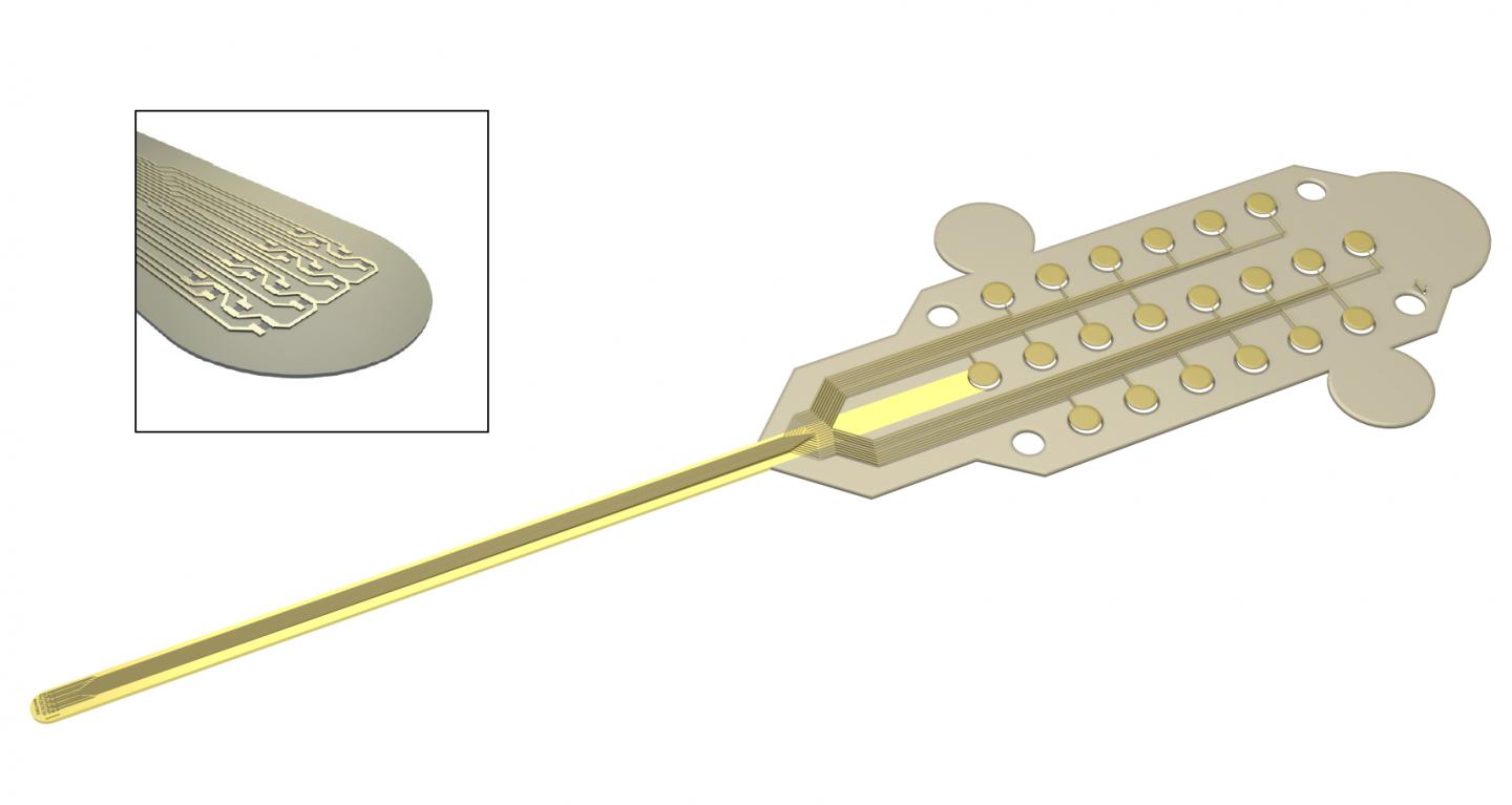
Measuring brain activity with precision is essential to developing further understanding of diseases such as epilepsy and disorders that affect brain function and motor control. Neural probes with high spatial resolution are needed for both recording and stimulating specific functional areas of the brain. Now, researchers from the Graphene Flagship have developed a new device for recording brain activity in high resolution while maintaining excellent signal to noise ratio (SNR). Based on graphene field-effect transistors, the flexible devices open up new possibilities for the development of functional implants and interfaces.

The research, published in 2D Materials, was a collaborative effort involving Flagship partners Technical University of Munich (TU Munich; Germany), Institut d’Investigacions Biomèdiques August Pi i Sunyer (IDIBAPS; Spain), Spanish National Research Council (CSIC; Spain), The Biomedical Research Networking Center in Bioengineering, Biomaterials and Nanomedicine (CIBER-BBN; Spain) and the Catalan Institute of Nanoscience and Nanotechnology (ICN2; Spain).

Caption: Graphene transistors integrated in a flexible neural probe enables electrical signals from neurons to be measured with high accuracy and density. Inset: The tip of the probe contains 16 flexible graphene transistors. Credit: ICN2

A March 27, 2017 Graphene Flagship press release on EurekAlert, which originated the news item, describes the work,  in more detail,

The devices were used to record the large signals generated by pre-epileptic activity in rats, as well as the smaller levels of brain activity during sleep and in response to visual light stimulation. These types of activities lead to much smaller electrical signals, and are at the level of typical brain activity. Neural activity is detected through the highly localised electric fields generated when neurons fire, so densely packed, ultra-small measuring devices is important for accurate brain readings.

The neural probes are placed directly on the surface of the brain, so safety is of paramount importance for the development of graphene-based neural implant devices. Importantly, the researchers determined that the graphene-based probes are non-toxic, and did not induce any significant inflammation.

Devices implanted in the brain as neural prosthesis for therapeutic brain stimulation technologies and interfaces for sensory and motor devices, such as artificial limbs, are an important goal for improving quality of life for patients. This work represents a first step towards the use of graphene in research as well as clinical neural devices, showing that graphene-based technologies can deliver the high resolution and high SNR needed for these applications.

First author Benno Blaschke (TU Munich) said “Graphene is one of the few materials that allows recording in a transistor configuration and simultaneously complies with all other requirements for neural probes such as flexibility, biocompability and chemical stability. Although graphene is ideally suited for flexible electronics, it was a great challenge to transfer our fabrication process from rigid substrates to flexible ones. The next step is to optimize the wafer-scale fabrication process and improve device flexibility and stability.”

Jose Antonio Garrido (ICN2), led the research. He said “Mechanical compliance is an important requirement for safe neural probes and interfaces. Currently, the focus is on ultra-soft materials that can adapt conformally to the brain surface. Graphene neural interfaces have shown already great potential, but we have to improve on the yield and homogeneity of the device production in order to advance towards a real technology. Once we have demonstrated the proof of concept in animal studies, the next goal will be to work towards the first human clinical trial with graphene devices during intraoperative mapping of the brain. This means addressing all regulatory issues associated to medical devices such as safety, biocompatibility, etc.”

Caption: The graphene-based neural probes were used to detect rats’ responses to visual stimulation, as well as neural signals during sleep. Both types of signals are small, and typically difficult to measure. Credit: ICN2

Here’s a link to and a citation for the paper,

Mapping brain activity with flexible graphene micro-transistors by Benno M Blaschke, Núria Tort-Colet, Anton Guimerà-Brunet, Julia Weinert, Lionel Rousseau, Axel Heimann, Simon Drieschner, Oliver Kempski, Rosa Villa, Maria V Sanchez-Vives. 2D Materials, Volume 4, Number 2 DOI https://doi.org/10.1088/2053-1583/aa5eff Published 24 February 2017

© 2017 IOP Publishing Ltd

This paper is behind a paywall.

Korea

While this research from Korea was published more recently, the probe itself has not been subjected to in vivo (animal testing). From an April 19, 2017 news item on ScienceDaily,

Electrodes placed in the brain record neural activity, and can help treat neural diseases like Parkinson’s and epilepsy. Interest is also growing in developing better brain-machine interfaces, in which electrodes can help control prosthetic limbs. Progress in these fields is hindered by limitations in electrodes, which are relatively stiff and can damage soft brain tissue.

Designing smaller, gentler electrodes that still pick up brain signals is a challenge because brain signals are so weak. Typically, the smaller the electrode, the harder it is to detect a signal. However, a team from the Daegu Gyeongbuk Institute of Science & Technology [DGIST} in Korea developed new probes that are small, flexible and read brain signals clearly.

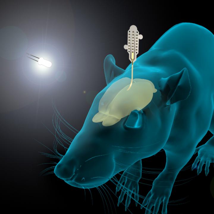
This is a pretty interesting way to illustrate the research,

Caption: Graphene and gold make a better brain probe. Credit: DGIST

An April 19, 2017 DGIST press release (also on EurekAlert), which originated the news item, expands on the theme (Note: A link has been removed),

The probe consists of an electrode, which records the brain signal. The signal travels down an interconnection line to a connector, which transfers the signal to machines measuring and analysing the signals.

The electrode starts with a thin gold base. Attached to the base are tiny zinc oxide nanowires, which are coated in a thin layer of gold, and then a layer of conducting polymer called PEDOT. These combined materials increase the probe’s effective surface area, conducting properties, and strength of the electrode, while still maintaining flexibility and compatibility with soft tissue.

Packing several long, thin nanowires together onto one probe enables the scientists to make a smaller electrode that retains the same effective surface area of a larger, flat electrode. This means the electrode can shrink, but not reduce signal detection. The interconnection line is made of a mix of graphene and gold. Graphene is flexible and gold is an excellent conductor. The researchers tested the probe and found it read rat brain signals very clearly, much better than a standard flat, gold electrode.

“Our graphene and nanowires-based flexible electrode array can be useful for monitoring and recording the functions of the nervous system, or to deliver electrical signals to the brain,” the researchers conclude in their paper recently published in the journal ACS Applied Materials and Interfaces.

The probe requires further clinical tests before widespread commercialization. The researchers are also interested in developing a wireless version to make it more convenient for a variety of applications.

Here’s a link to and a citation for the paper,

Enhancement of Interface Characteristics of Neural Probe Based on Graphene, ZnO Nanowires, and Conducting Polymer PEDOT by Mingyu Ryu, Jae Hoon Yang, Yumi Ahn, Minkyung Sim, Kyung Hwa Lee, Kyungsoo Kim, Taeju Lee, Seung-Jun Yoo, So Yeun Kim, Cheil Moon, Minkyu Je, Ji-Woong Choi, Youngu Lee, and Jae Eun Jang. ACS Appl. Mater. Interfaces, 2017, 9 (12), pp 10577–10586 DOI: 10.1021/acsami.7b02975 Publication Date (Web): March 7, 2017

Copyright © 2017 American Chemical Society

This paper is behind a paywall.

Developing cortical implants for future speech neural prostheses

I’m guessing that graphene will feature in these proposed cortical implants since the project leader is a member of the Graphene Flagship’s Biomedical Technologies Work Package. (For those who don’t know, the Graphene Flagship is one of two major funding initiatives each receiving funding of 1B Euros over 10 years from the European Commission as part of their FET [Future and Emerging Technologies)] Initiative.)  A Jan. 12, 2017 news item on Nanowerk announces the new project (Note: A link has been removed),

BrainCom is a FET Proactive project, funded by the European Commission with 8.35M€ [8.3 million Euros] for the next 5 years, holding its Kick-off meeting on January 12-13 at ICN2 (Catalan Institute of Nanoscience and Nanotechnology) and the UAB [ Universitat Autònoma de Barcelona]. This project, coordinated by ICREA [Catalan Institution for Research and Advanced Studies] Research Prof. Jose A. Garrido from ICN2, will permit significant advances in understanding of cortical speech networks and the development of speech rehabilitation solutions using innovative brain-computer interfaces.

A Jan. 12, 2017 ICN2 press release, which originated the news item expands on the theme (it is a bit repetitive),

More than 5 million people worldwide suffer annually from aphasia, an extremely invalidating condition in which patients lose the ability to comprehend and formulate language after brain damage or in the course of neurodegenerative disorders. Brain-computer interfaces (BCIs), enabled by forefront technologies and materials, are a promising approach to treat patients with aphasia. The principle of BCIs is to collect neural activity at its source and decode it by means of electrodes implanted directly in the brain. However, neurorehabilitation of higher cognitive functions such as language raises serious issues. The current challenge is to design neural implants that cover sufficiently large areas of the brain to allow for reliable decoding of detailed neuronal activity distributed in various brain regions that are key for language processing.

BrainCom is a FET Proactive project funded by the European Commission with 8.35M€ for the next 5 years. This interdisciplinary initiative involves 10 partners including technologists, engineers, biologists, clinicians, and ethics experts. They aim to develop a new generation of neuroprosthetic cortical devices enabling large-scale recordings and stimulation of cortical activity to study high level cognitive functions. Ultimately, the BraimCom project will seed a novel line of knowledge and technologies aimed at developing the future generation of speech neural prostheses. It will cover different levels of the value chain: from technology and engineering to basic and language neuroscience, and from preclinical research in animals to clinical studies in humans.

This recently funded project is coordinated by ICREA Prof. Jose A. Garrido, Group Leader of the Advanced Electronic Materials and Devices Group at the Institut Català de Nanociència i Nanotecnologia (Catalan Institute of Nanoscience and Nanotechnology – ICN2) and deputy leader of the Biomedical Technologies Work Package presented last year in Barcelona by the Graphene Flagship. The BrainCom Kick-Off meeting is held on January 12-13 at ICN2 and the Universitat Autònoma de Barcelona (UAB).

Recent developments show that it is possible to record cortical signals from a small region of the motor cortex and decode them to allow tetraplegic [also known as, quadriplegic] people to activate a robotic arm to perform everyday life actions. Brain-computer interfaces have also been successfully used to help tetraplegic patients unable to speak to communicate their thoughts by selecting letters on a computer screen using non-invasive electroencephalographic (EEG) recordings. The performance of such technologies can be dramatically increased using more detailed cortical neural information.

BrainCom project proposes a radically new electrocorticography technology taking advantage of unique mechanical and electrical properties of novel nanomaterials such as graphene, 2D materials and organic semiconductors.  The consortium members will fabricate ultra-flexible cortical and intracortical implants, which will be placed right on the surface of the brain, enabling high density recording and stimulation sites over a large area. This approach will allow the parallel stimulation and decoding of cortical activity with unprecedented spatial and temporal resolution.

These technologies will help to advance the basic understanding of cortical speech networks and to develop rehabilitation solutions to restore speech using innovative brain-computer paradigms. The technology innovations developed in the project will also find applications in the study of other high cognitive functions of the brain such as learning and memory, as well as other clinical applications such as epilepsy monitoring.

The BrainCom project Consortium members are:

  • Catalan Institute of Nanoscience and Nanotechnology (ICN2) – Spain (Coordinator)
  • Institute of Microelectronics of Barcelona (CNM-IMB-CSIC) – Spain
  • University Grenoble Alpes – France
  • ARMINES/ Ecole des Mines de St. Etienne – France
  • Centre Hospitalier Universitaire de Grenoble – France
  • Multichannel Systems – Germany
  • University of Geneva – Switzerland
  • University of Oxford – United Kingdom
  • Ludwig-Maximilians-Universität München – Germany
  • Wavestone – Luxembourg

There doesn’t seem to be a website for the project but there is a BrainCom webpage on the European Commission’s CORDIS (Community Research and Development Information Service) website.

Graphene Flagship high points

The European Union’s Graphene Flagship project has provided a series of highlights in place of an overview for the project’s ramp-up phase (in 2013 the Graphene Flagship was announced as one of two winners of a science competition, the other winner was the Human Brain Project, with two prizes of 1B Euros for each project). Here are the highlights from the April 19, 2016 Graphene Flagship press release,

Graphene and Neurons – the Best of Friends

Flagship researchers have shown that it is possible to interface untreated graphene with neuron cells whilst maintaining the integrity of these vital cells [1]. This result is a significant first step towards using graphene to produce better deep brain implants which can both harness and control the brain.

Graphene and Neurons
 

This paper emerged from the Graphene Flagship Work Package Health and Environment. Prof. Prato, the WP leader from the University of Trieste in Italy, commented that “We are currently involved in frontline research in graphene technology towards biomedical applications, exploring the interactions between graphene nano- and micro-sheets with the sophisticated signalling machinery of nerve cells. Our work is a first step in that direction.”

[1] Fabbro A., et al., Graphene-Based Interfaces do not Alter Target Nerve Cells. ACS Nano, 10 (1), 615 (2016).

Pressure Sensing with Graphene: Quite a Squeeze

The Graphene Flagship developed a small, robust, highly efficient squeeze film pressure sensor [2]. Pressure sensors are present in most mobile handsets and by replacing current sensor membranes with a graphene membrane they allow the sensor to decrease in size and significantly increase its responsiveness and lifetime.

Discussing this work which emerged from the Graphene Flagship Work Package Sensors is the paper’s lead author, Robin Dolleman from the Technical University of Delft in The Netherlands “After spending a year modelling various systems the idea of the squeeze-film pressure sensor was formed. Funding from the Graphene Flagship provided the opportunity to perform the experiments and we obtained very good results. We built a squeeze-film pressure sensor from 31 layers of graphene, which showed a 45 times higher response than silicon based devices, while reducing the area of the device by a factor of 25. Currently, our work is focused on obtaining similar results on monolayer graphene.”


[2] Dolleman R. J. et al., Graphene Squeeze-Film Pressure Sensors. Nano Lett., 16, 568 (2016)

Frictionless Graphene


Image caption: A graphene nanoribbon was anchored at the tip of a atomic force microscope and dragged over a gold surface. The observed friction force was extremely low.

Image caption: A graphene nanoribbon was anchored at the tip of a atomic force microscope and dragged over a gold surface. The observed friction force was extremely low.

Research done within the Graphene Flagship, has observed the onset of superlubricity in graphene nanoribbons sliding on a surface, unravelling the role played by ribbon size and elasticity [3]. This important finding opens up the development potential of nanographene frictionless coatings. This research lead by the Graphene Flagship Work Package Nanocomposites also involved researchers from Work Package Materials and Work Package Health and the Environment, a shining example of the inter-disciplinary, cross-collaborative approach to research undertaken within the Graphene Flagship. Discussing this further is the Work Package Nanocomposites Leader, Dr Vincenzo Palermo from CNR National Research Council, Italy “Strengthening the collaboration and interactions with other Flagship Work Packages created added value through a strong exchange of materials, samples and information”.

[3] Kawai S., et al., Superlubricity of graphene nanoribbons on gold surfaces. Science. 351, 6276, 957 (2016) 

​Graphene Paddles Forward

Work undertaken within the Graphene Flagship saw Spanish automotive interiors specialist, and Flagship partner, Grupo Antolin SA work in collaboration with Roman Kayaks to develop an innovative kayak that incorporates graphene into its thermoset polymeric matrices. The use of graphene and related materials results in a significant increase in both impact strength and stiffness, improving the resistance to breakage in critical areas of the boat. Pushing the graphene canoe well beyond the prototype demonstration bubble, Roman Kayaks chose to use the K-1 kayak in the Canoe Marathon World Championships held in September in Gyor, Hungary where the Graphene Canoe was really put through its paces.

Talking further about this collaboration from the Graphene Flagship Work Package Production is the WP leader, Dr Ken Teo from Aixtron Ltd., UK “In the Graphene Flagship project, Work Package Production works as a technology enabler for real-world applications. Here we show the worlds first K-1 kayak (5.2 meters long), using graphene related materials developed by Grupo Antolin. We are very happy to see that graphene is creating value beyond traditional industries.” 

​Graphene Production – a Kitchen Sink Approach

Researchers from the Graphene Flagship have devised a way of producing large quantities of graphene by separating graphite flakes in liquids with a rotating tool that works in much the same way as a kitchen blender [4]. This paves the way to mass production of high quality graphene at a low cost.

The method was produced within the Graphene Flagship Work Package Production and is talked about further here by the WP deputy leader, Prof. Jonathan Coleman from Trinity College Dublin, Ireland “This technique produced graphene at higher rates than most other methods, and produced sheets of 2D materials that will be useful in a range of applications, from printed electronics to energy generation.” 

[4] Paton K.R., et al., Scalable production of large quantities of defect-free few-layer graphene by shear exfoliation in liquids. Nat. Mater. 13, 624 (2014).

Flexible Displays – Rolled Up in your Pocket

Working with researchers from the Graphene Flagship the Flagship partner, FlexEnable, demonstrated the world’s first flexible display with graphene incorporated into its pixel backplane. Combined with an electrophoretic imaging film, the result is a low-power, durable display suitable for use in many and varied environments.

Emerging from the Graphene Flagship Work Package Flexible Electronics this illustrates the power of collaboration.  Talking about this is the WP leader Dr Henrik Sandberg from the VTT Technical Research Centre of Finland Ltd., Finland “Here we show the power of collaboration. To deliver these flexible demonstrators and prototypes we have seen materials experts working together with components manufacturers and system integrators. These devices will have a potential impact in several emerging fields such as wearables and the Internet of Things.”

​Fibre-Optics Data Boost from Graphene

A team of researches from the Graphene Flagship have demonstrated high-performance photo detectors for infrared fibre-optic communication systems based on wafer-scale graphene [5]. This can increase the amount of information transferred whilst at the same time make the devises smaller and more cost effective.

Discussing this work which emerged from the Graphene Flagship Work Package Optoelectronics is the paper’s lead author, Daniel Schall from AMO, Germany “Graphene has outstanding properties when it comes to the mobility of its electric charge carriers, and this can increase the speed at which electronic devices operate.”

[5] Schall D., et al., 50 GBit/s Photodetectors Based on Wafer-Scale Graphene for Integrated Silicon Photonic Communication Systems. ACS Photonics. 1 (9), 781 (2014)

​Rechargeable Batteries with Graphene

A number of different research groups within the Graphene Flagship are working on rechargeable batteries. One group has developed a graphene-based rechargeable battery of the lithium-ion type used in portable electronic devices [6]. Graphene is incorporated into the battery anode in the form of a spreadable ink containing a suspension of graphene nanoflakes giving an increased energy efficiency of 20%. A second group of researchers have demonstrated a lithium-oxygen battery with high energy density, efficiency and stability [7]. They produced a device with over 90% efficiency that may be recharged more than 2,000 times. Their lithium-oxygen cell features a porous, ‘fluffy’ electrode made from graphene together with additives that alter the chemical reactions at work in the battery.

Graphene Flagship researchers show how the 2D material graphene can improve the energy capacity, efficiency and stability of lithium-oxygen batteries.

Both devices were developed in different groups within the Graphene Flagship Work Package Energy and speaking of the technology further is Prof. Clare Grey from Cambridge University, UK “What we’ve achieved is a significant advance for this technology, and suggests whole new areas for research – we haven’t solved all the problems inherent to this chemistry, but our results do show routes forward towards a practical device”.

[6] Liu T., et al. Cycling Li-O2 batteries via LiOH formation and decomposition. Science. 350, 6260, 530 (2015)

[7] Hassoun J., et al., An Advanced Lithium-Ion Battery Based on a Graphene Anode and a Lithium Iron Phosphate Cathode. Nano Lett., 14 (8), 4901 (2014)

Graphene – What and Why?

Graphene is a two-dimensional material formed by a single atom-thick layer of carbon, with the carbon atoms arranged in a honeycomb-like lattice. This transparent, flexible material has a number of unique properties. For example, it is 100 times stronger than steel, and conducts electricity and heat with great efficiency.

A number of practical applications for graphene are currently being developed. These include flexible and wearable electronics and antennas, sensors, optoelectronics and data communication systems, medical and bioengineering technologies, filtration, super-strong composites, photovoltaics and energy storage.

Graphene and Beyond

The Graphene Flagship also covers other layered materials, as well as hybrids formed by combining graphene with these complementary materials, or with other materials and structures, ranging from polymers, to metals, cement, and traditional semiconductors such as silicon. Graphene is just the first of thousands of possible single layer materials. The Flagship plans to accelerate their journey from laboratory to factory floor.

Especially exciting is the possibility of stacking monolayers of different elements to create materials not found in nature, with properties tailored for specific applications. Such composite layered materials could be combined with other nanomaterials, such as metal nanoparticles, in order to further enhance their properties and uses.​

Graphene – the Fruit of European Scientific Excellence

Europe, North America and Asia are all active centres of graphene R&D, but Europe has special claim to be at the centre of this activity. The ground-breaking experiments on graphene recognised in the award of the 2010 Nobel Prize in Physics were conducted by European physicists, Andre Geim and Konstantin Novoselov, both at Manchester University. Since then, graphene research in Europe has continued apace, with major public funding for specialist centres, and the stimulation of academic-industrial partnerships devoted to graphene and related materials. It is European scientists and engineers who as part of the Graphene Flagship are closely coordinating research efforts, and accelerating the transfer of layered materials from the laboratory to factory floor.

For anyone who would like links to the published papers, you can check out an April 20, 2016 news item featuring the Graphene Flagship highlights on Nanowerk.

With over 150 partners from over 20 countries, the European Union’s Graphene Flagship research initiative unveils its work package devoted to biomedical technologies

An April 11, 2016 news item on Nanowerk announces the Graphene Flagship’s latest work package,

With a budget of €1 billion, the Graphene Flagship represents a new form of joint, coordinated research on an unprecedented scale, forming Europe’s biggest ever research initiative. It was launched in 2013 to bring together academic and industrial researchers to take graphene from the realm of academic laboratories into European society in the timeframe of 10 years. The initiative currently involves over 150 partners from more than 20 European countries. The Graphene Flagship, coordinated by Chalmers University of Technology (Sweden), is implemented around 15 scientific Work Packages on specific science and technology topics, such as fundamental science, materials, health and environment, energy, sensors, flexible electronics and spintronics.

Today [April 11, 2016], the Graphene Flagship announced in Barcelona the creation of a new Work Package devoted to Biomedical Technologies, one emerging application area for graphene and other 2D materials. This initiative is led by Professor Kostas Kostarelos, from the University of Manchester (United Kingdom), and ICREA Professor Jose Antonio Garrido, from the Catalan Institute of Nanoscience and Nanotechnology (ICN2, Spain). The Kick-off event, held in the Casa Convalescència of the Universitat Autònoma de Barcelona (UAB), is co-organised by ICN2 (ICREA Prof Jose Antonio Garrido), Centro Nacional de Microelectrónica (CNM-IMB-CSIC, CIBER-BBN; CSIC Tenured Scientist Dr Rosa Villa), and Institut d’Investigacions Biomèdiques August Pi i Sunyer (IDIBAPS; ICREA Prof Mavi Sánchez-Vives).

An April 11, 2016 ICN2 press release, which originated the news item, provides more detail about the Biomedical Technologies work package and other work packages,

The new Work Package will focus on the development of implants based on graphene and 2D-materials that have therapeutic functionalities for specific clinical outcomes, in disciplines such as neurology, ophthalmology and surgery. It will include research in three main areas: Materials Engineering; Implant Technology & Engineering; and Functionality and Therapeutic Efficacy. The objective is to explore novel implants with therapeutic capacity that will be further developed in the next phases of the Graphene Flagship.

The Materials Engineering area will be devoted to the production, characterisation, chemical modification and optimisation of graphene materials that will be adopted for the design of implants and therapeutic element technologies. Its results will be applied by the Implant Technology and Engineering area on the design of implant technologies. Several teams will work in parallel on retinal, cortical, and deep brain implants, as well as devices to be applied in the periphery nerve system. Finally, The Functionality and Therapeutic Efficacy area activities will centre on development of devices that, in addition to interfacing the nerve system for recording and stimulation of electrical activity, also have therapeutic functionality.

Stimulation therapies will focus on the adoption of graphene materials in implants with stimulation capabilities in Parkinson’s, blindness and epilepsy disease models. On the other hand, biological therapies will focus on the development of graphene materials as transport devices of biological molecules (nucleic acids, protein fragments, peptides) for modulation of neurophysiological processes. Both approaches involve a transversal innovation environment that brings together the efforts of different Work Packages within the Graphene Flagship.

A leading role for Barcelona in Graphene and 2D-Materials

The kick-off meeting of the new Graphene Flagship Work Package takes place in Barcelona because of the strong involvement of local institutions and the high international profile of Catalonia in 2D-materials and biomedical research. Institutions such as the Catalan Institute of Nanoscience and Nanotechnology (ICN2) develop frontier research in a supportive environment which attracts talented researchers from abroad, such as ICREA Research Prof Jose Antonio Garrido, Group Leader of the ICN2 Advanced Electronic Materials and Devices Group and now also Deputy Leader of the Biomedical Technologies Work Package. Until summer 2015 he was leading a research group at the Technische Universität München (Germany).

Further Graphene Flagship events in Barcelona are planned; in May 2016 ICN2 will also host a meeting of the Spintronics Work Package. ICREA Prof Stephan Roche, Group Leader of the ICN2 Theoretical and Computational Nanoscience Group, is the deputy leader of this Work Package led by Prof Bart van Wees, from the University of Groningen (The Netherlands). Another Work Package, on optoelectronics, is led by Prof Frank Koppens from the Institute of Photonic Sciences (ICFO, Spain), with Prof Andrea Ferrari from the University of Cambridge (United Kingdom) as deputy. Thus a number of prominent research institutes in Barcelona are deeply involved in the coordination of this European research initiative.

Kostas Kostarelos, the leader of the Biomedical Technologies Graphene Flagship work package, has been mentioned here before in the context of his blog posts for The Guardian science blog network (see my Aug. 7, 2014 post for a link to his post on metaphors used in medicine).

Tempest in a teapot or a sign of things to come? UK’s National Graphene Institute kerfuffle

A scandal-in-the-offing, intellectual property, miffed academics, a chortling businessman, graphene, and much more make this a fascinating story.

Before launching into the main attractions, those unfamiliar with the UK graphene effort might find this background informal useful. Graphene, was first isolated at the University of Manchester in 2004 by scientists Andre Geim* and Konstantin Novoselov, Russian immigrants, both of whom have since become Nobel laureates and knights of the realm. The excitement in the UK and elsewhere is due to graphene’s extraordinary properties which could lead to transparent electronics, foldable/bendable electronics, better implants, efficient and inexpensive (they hope) water filters, and more. The UK government has invested a lot of money in graphene as has the European Union (1B Euros in the Graphene Flagship) in the hope that huge economic benefits will be reaped.

Dexter Johnson’s March 15, 2016 posting on his Nanoclast blog (on the IEEE [Institute for Electrical and Electronics Engineers] website) provides details about the situation (Note: Links have been removed),

A technology that, a year ago, was being lauded as the “first commercially viable consumer product” using graphene now appears to be caught up in an imbroglio over who owns its intellectual property rights. The resulting controversy has left the research institute behind the technology in a bit of a public relations quagmire.

The venerable UK publication The Sunday Times reported this week on what appeared to be a mutiny occurring at the National Graphene Institute (NGI) located at the University of Manchester. Researchers at the NGI had reportedly stayed away from working at the institute’s gleaming new $71 million research facility over fears that their research was going to end up in the hands of foreign companies, in particular a Taiwan-based company called BGT Materials.

The “first commercially viable consumer product” noted in Dexter’s posting was a graphene-based lightbulb which was announced by the NGI to much loud crowing in March 2015 (see my March 30, 2015 posting). The company producing the lightbulb was announced as “… Graphene Lighting PLC is a spin-out based on a strategic partnership with the National Graphene Institute (NGI) at The University of Manchester to create graphene applications.” There was no mention of BGT.

Dexter describes the situation from the BGT perspective (from his March 15, 2016 posting), Note: Links have been removed,

… BGT did not demur when asked by  the Times whether it owned the technology. In fact, Chung Ping Lai, BGT’s CEO, claimed it was his company that had invented the technology for the light bulb and not the NGI. The Times report further stated that Lai controls all the key patents and claims to be delighted with his joint venture with the university. “I believe in luck and I have had luck in Manchester,” Lai told the Times.

With companies outside the UK holding majority stakes in the companies spun out of the NGI—allowing them to claim ownership of the technologies developed at the institute—one is left to wonder what was the purpose of the £50 million (US $79 million) earmarked for graphene research in the UK more than four years ago? Was it to develop a local economy based around graphene—a “Graphene Valley”, if you will? Or was it to prop up the local construction industry through the building of shiny new buildings that reportedly few people occupy? That’s the charge leveled by Andre Geim, Nobel laureate for his discovery of graphene, and NGI’s shining star. Geim reportedly described the new NGI building as: “Money put in the British building industry rather than science.”

Dexter ends his March 15, 2016 posting with an observation  that will seem familiar to Canadians,

Now, it seems the government’s eagerness to invest in graphene research—or at least, the facilities for conducting that research—might have ended up bringing it to the same place as its previous lack of investment: the science is done in the UK and the exploitation of the technology is done elsewhere.

The March 13, 2016 Sunday Times article [ETA on April 3, 2016: This article is now behind a paywall] by Tom Harper, Jon Ungoed-Thomas and Michael Sheridan, which seems to be the source of Dexter’s posting, takes a more partisan approach,

ACADEMICS are boycotting a top research facility after a company linked to China was given access to lucrative confidential material from one of Britain’s greatest scientific breakthroughs.

Some scientists at Manchester University working on graphene, a wonder substance 200 times stronger than steel, refuse to work at the new £61m national institution, set up to find ways to exploit the material, amid concerns over a deal struck between senior university management and BGT Materials.

The academics are concerned that the National Graphene Institute (NGI), which was opened last year by George Osborne, the chancellor, and forms one of the key planks of his “northern powerhouse” industrial strategy, does not have the necessary safeguards to protect their confidential research, which could revolutionise the electronics, energy, health and building industries.

BGT, which is controlled by a Taiwanese businessman, subsequently agreed to work with a Chinese manufacturing company and university to develop similar graphene technology.

BGT says its work in Manchester has been successful and it is “offensive” and “untrue” to suggest that it would unfairly use intellectual property. The university say there is no evidence “whatsoever” of unfair use of confidential information. Manchester says it is understandable that some scientists are cautious about the collaborative environment of the new institute. But one senior academic said the arrangement with BGT had caused the university’s graphene research to descend into “complete anarchy”.

The academic said: “The NGI is a national facility, and why should we use it for a company, which is not even an English [owned] company? How much [intellectual property] is staying in England and how much is going to Taiwan?”

The row highlights concerns that the UK has dawdled in developing one of its greatest discoveries. Nearly 50% of ­graphene-related patents have been filed in China, and just 1% in Britain.

Manchester signed a £5m “research collaboration agreement” with BGT Materials in October 2013. Although the company is controlled by a Taiwanese businessman, Chung-ping Lai, the university does have a 17.5% shareholding.

Manchester claimed that the commercial deal would “attract a significant number of jobs to the city” and “benefit the UK economy”.

However, an investigation by The Sunday Times has established:

Only four jobs have been created as a result of the deal and BGT has not paid the full £5m due under the agreement after two projects were cancelled.

Pictures sent to The Sunday Times by a source at the university last month show that the offices at the NGI [National Graphene Institute], which can accommodate 120 staff, were deserted.

British-based businessmen working with graphene have also told The Sunday Times of their concerns about the institute’s information security. Tim Harper, a Manchester-based graphene entrepreneur, said: “We looked at locating there [at the NGI] but we take intellectual property extremely seriously and it is a problem locating in such a facility.

“If you don’t have control over your computer systems or the keys to your lab, then you’ve got a problem.”

I recommend reading Dexter’s post and the Sunday Times article as they provide some compelling insight into the UK situation vis à vis nanotechnology, science, and innovation.

*’Gheim’ corrected to ‘Geim’ on March 30, 2016.

Graphene and neurons in a UK-Italy-Spain collaboration

There’s been a lot of talk about using graphene-based implants in the brain due to the material’s flexibility along with its other properties. A step forward has been taking according to a Jan. 29, 2016 news item on phys.org,

Researchers have successfully demonstrated how it is possible to interface graphene – a two-dimensional form of carbon – with neurons, or nerve cells, while maintaining the integrity of these vital cells. The work may be used to build graphene-based electrodes that can safely be implanted in the brain, offering promise for the restoration of sensory functions for amputee or paralysed patients, or for individuals with motor disorders such as epilepsy or Parkinson’s disease.

A Jan. 29, 2016 Cambridge University press release (also on EurekAlert), which originated the news item, provides more detail,

Previously, other groups had shown that it is possible to use treated graphene to interact with neurons. However the signal to noise ratio from this interface was very low. By developing methods of working with untreated graphene, the researchers retained the material’s electrical conductivity, making it a significantly better electrode.

“For the first time we interfaced graphene to neurons directly,” said Professor Laura Ballerini of the University of Trieste in Italy. “We then tested the ability of neurons to generate electrical signals known to represent brain activities, and found that the neurons retained their neuronal signalling properties unaltered. This is the first functional study of neuronal synaptic activity using uncoated graphene based materials.”

Our understanding of the brain has increased to such a degree that by interfacing directly between the brain and the outside world we can now harness and control some of its functions. For instance, by measuring the brain’s electrical impulses, sensory functions can be recovered. This can be used to control robotic arms for amputee patients or any number of basic processes for paralysed patients – from speech to movement of objects in the world around them. Alternatively, by interfering with these electrical impulses, motor disorders (such as epilepsy or Parkinson’s) can start to be controlled.

Scientists have made this possible by developing electrodes that can be placed deep within the brain. These electrodes connect directly to neurons and transmit their electrical signals away from the body, allowing their meaning to be decoded.

However, the interface between neurons and electrodes has often been problematic: not only do the electrodes need to be highly sensitive to electrical impulses, but they need to be stable in the body without altering the tissue they measure.

Too often the modern electrodes used for this interface (based on tungsten or silicon) suffer from partial or complete loss of signal over time. This is often caused by the formation of scar tissue from the electrode insertion, which prevents the electrode from moving with the natural movements of the brain due to its rigid nature.

Graphene has been shown to be a promising material to solve these problems, because of its excellent conductivity, flexibility, biocompatibility and stability within the body.

Based on experiments conducted in rat brain cell cultures, the researchers found that untreated graphene electrodes interfaced well with neurons. By studying the neurons with electron microscopy and immunofluorescence the researchers found that they remained healthy, transmitting normal electric impulses and, importantly, none of the adverse reactions which lead to the damaging scar tissue were seen.

According to the researchers, this is the first step towards using pristine graphene-based materials as an electrode for a neuro-interface. In future, the researchers will investigate how different forms of graphene, from multiple layers to monolayers, are able to affect neurons, and whether tuning the material properties of graphene might alter the synapses and neuronal excitability in new and unique ways. “Hopefully this will pave the way for better deep brain implants to both harness and control the brain, with higher sensitivity and fewer unwanted side effects,” said Ballerini.

“We are currently involved in frontline research in graphene technology towards biomedical applications,” said Professor Maurizio Prato from the University of Trieste. “In this scenario, the development and translation in neurology of graphene-based high-performance biodevices requires the exploration of the interactions between graphene nano- and micro-sheets with the sophisticated signalling machinery of nerve cells. Our work is only a first step in that direction.”

“These initial results show how we are just at the tip of the iceberg when it comes to the potential of graphene and related materials in bio-applications and medicine,” said Professor Andrea Ferrari, Director of the Cambridge Graphene Centre. “The expertise developed at the Cambridge Graphene Centre allows us to produce large quantities of pristine material in solution, and this study proves the compatibility of our process with neuro-interfaces.”

The research was funded by the Graphene Flagship [emphasis mine],  a European initiative which promotes a collaborative approach to research with an aim of helping to translate graphene out of the academic laboratory, through local industry and into society.

Here’s a link to and a citation for the paper,

Graphene-Based Interfaces Do Not Alter Target Nerve Cells by Alessandra Fabbro, Denis Scaini, Verónica León, Ester Vázquez, Giada Cellot, Giulia Privitera, Lucia Lombardi, Felice Torrisi, Flavia Tomarchio, Francesco Bonaccorso, Susanna Bosi, Andrea C. Ferrari, Laura Ballerini, and Maurizio Prato. ACS Nano, 2016, 10 (1), pp 615–623 DOI: 10.1021/acsnano.5b05647 Publication Date (Web): December 23, 2015

Copyright © 2015 American Chemical Society

This paper is behind a paywall.

There are a couple things I found a bit odd about this project. First, all of the funding is from the Graphene Flagship initiative. I was expecting to see at least some funding from the European Union’s other mega-sized science initiative, the Human Brain Project. Second, there was no mention of Spain nor were there any quotes from the Spanish researchers. For the record, the Spanish institutions represented were: University of Castilla-La Mancha, Carbon Nanobiotechnology Laboratory, and the Basque Foundation for Science.