Tag Archives: Horizon 2020 programme

Art and 5G at museums in Turin (Italy)

Caption: In the framework of EU-funded project 5GTours, R1 humanoid robot tested at GAM (Turin) its ability to navigate and interact with visitors at the 20th-century collections, accompanying them to explore a selection of the museum’s most representative works, such as Andy Warhol’s “Orange car crash”. The robot has been designed and developed by IIT, while the 5G connection was set up by TIM using Ericsson technology.. Credit: IIT-Istituto Italiano di Tecnologia/GAM

This May 27, 2022 Istituto Italiano di Tecnologia (IIT) press release on EurekAlert offers an intriguing view into the potential for robots in art galleries,

Robotics, 5G and art: during the month of May visitors to the Turin’s art museums, Turin Civic Gallery of Modern and Contemporary Art (GAM) and Turin City Museum of Ancient Art (Palazzo Madama), had the opportunity to be part of various experiments based on 5G-network technology. Interactive technologies and robots were the focus of an innovative enjoyment of the art collections, with a great appreciation from the public.

Visitors to the GAM and to Palazzo Madama were provided with a number of engaging interactive experiences made possible through a significant collaboration between public and private organisations, which have been working together for more than three years to experiment the potential of new 5G technology in the framework of the EU-funded project 5GTours (https://5gtours.eu/).

The demonstrations set up in Turin led to the creation of innovative applications in the tourism and culture sectors that can easily be replicated in any artistic or museum context.

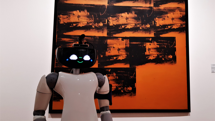
In both venues, visitors had the opportunity to meet R1, the humanoid robot designed by the IIT-Istituto Italiano di Tecnologia (Italian Institute of Technology) in Genova and created to operate in domestic and professional environments, whose autonomous and remote navigation system is well integrated with the bandwidth and latency offered by a 5G connection. R1, the robot – 1 metre 25 cm in height, weighing 50 kg, made 50% from plastic and 50% from carbon fibre and metal – is able to describe the works and answer questions regarding the artist or the period in history to which the work belongs. 5G connectivity is required in order to transmit the considerable quantity of data generated by the robot’s sensors and the algorithms that handle environmental perception, autonomous navigation and dialogue to external processing systems with extremely rapid response times.

At Palazzo Madama R1 humanoid robot led a guided tour of the Ceramics Room, while at GAM it was available to visitors of the twentieth-century collections, accompanying them to explore a selection of the museum’s most representative works. R1 robot explained and responded to questions about six relevant paintings: Felice Casorati’s “Daphne a Pavarolo”, Osvaldo Lucini’s “Uccello 2”, Marc Chagall’s “Dans mon pays”, Alberto Burri’s “Sacco”, Andy Warhol’s “Orange car crash” and Mario Merz’s “Che Fare?”.

Moreover, visitors – with the use of Meta Quest visors also connected to the 5G network – were required to solve a puzzle, putting the paintings in the Guards’ Room back into their frames. With these devices, the works in the hall, which in reality cannot be touched, can be handled and moved virtually. Lastly, the visitors involved had the opportunity to visit the underground spaces of Palazzo Madama with the mini-robot Double 3, which uses the 5G network to move reactively and precisely within the narrow spaces.

At GAM a class of students from a local school were able to remotely connect and manoeuvre the mini-robot Double 3 located in the rooms of the twentieth-century collections at the GAM directly from their classroom. A treasure hunt held in the museum with the participants never leaving the school.

In the Educational Area, a group of youngsters had the opportunity of collaborating in the painting of a virtual work of art on a large technological wall, drawing inspiration from works by Nicola De Maria.

The 5G network solutions created at the GAM and at Palazzo Madama by TIM [Telecom Italia] with Ericsson technology in collaboration with the City of Turin and the Turin Museum Foundation, guarantee constant high-speed transmission and extremely low latency. These solutions, which comply with 3GPP standard, are extremely flexible in terms of setting up and use. In the case of Palazzo Madama, a UNESCO World Heritage Site, tailor-made installations were designed, using apparatus and solutions that perfectly integrate with the museum spaces, while at the same time guaranteeing extremely high performance. At the GAM, the Radio Dot System has been implemented, a new 5G solution from Ericsson that is small enough to be held in the palm of a hand, and that provides network coverage and performance required for busy indoor areas. Thanks to these activities, Turin is ever increasingly playing a role as an open-air laboratory for urban innovation; since 2021 it has been the location of the “House of Emerging Technology – CTE NEXT”, a veritable centre for technology transfer via 5G and for emerging technologies coordinated by the Municipality of Turin and financed by the Ministry for Economic Development.

Through these solutions, Palazzo Madama and the GAM are now unique examples of technology in Italy and a rare example on a European level of museum buildings with full 5G coverage.

The experience was the result of the project financed by the European Union, 5G-TOURS 5G smarT mObility, media and e-health for toURists and citizenS”, the city of Turin – Department and Directorate of Innovation, in collaboration with the Department of Culture – Ericsson, TIM [Telecom Italia], the Turin Museum Foundation and the IIT-Istituto Italiano di Tecnologia (Italian Institute of Technology) of Genova, with the contribution of the international partners Atos and Samsung. The 5G coverage within the two museums was set up by TIM using Ericsson technology, solutions that perfectly integrated with the areas within the two museums structures.

Just in case you missed the link in the press release, you can find more information about this European Union Horizon 2020-funded 5G project, here at 5G TOURS (SmarT mObility, media and e-health for toURists and citizenS). You can find out more about the grant, e.g., this project sunset in July 2022, here.

The long road to commercializing nanotechnology-enabled products in Europe: the IP Nanoker Project

IP Nanoker, a nanotechnology commercialization project, was a European Union 7th Framework Programme-funded project from 2005 – 2009. So, how does IP Nanoker end up in a June 11, 2014 news item on Nanowerk? The road to commercialization is not only long, it is also winding as this news item points out in an illuminating fashion,

Superior hip, knee and dental implants, a new generation of transparent airplane windows and more durable coatings for automotive engines are just some of the products made possible – and cheaper – by the EU-funded IP NANOKER project. Many of these materials are now heading to market, boosting Europe’s competitiveness and creating jobs.

Launched back in 2005, the four-year project set out to build upon Europe’s expertise and knowledge in nanoceramics and nanocomposites.

Nanocomposites entirely made up of ceramic and metallic nanoscale particles – particles that are usually between 1 and 100 nanometres in size – are a broad new class of engineered materials that combine excellent mechanical performance with critical functionalities such as transparency, biocompatibility, and wear resistance.

These materials offer improvements over conventional materials. For some advanced optical applications – such as windows for aircraft – glass is too brittle. Nanoceramics offer both transparency and toughness, and thanks to IP NANOKER, can now be manufactured at a significantly reduced cost.
Indeed, one of the most important outcomes of IP NANOKER has been the development of new dense nanostructured materials as hard as diamond. The fabrication of these super hard materials require extreme conditions of high temperature and pressure, which is why IP NANOKER project partners developed a customised Spark Plasma Sintering machine.

“This new equipment is the largest in the world (12 metres high, 6 metres wide and 5 metres deep), and features a pressing force up to 400 tonnes and will allow the fabrication of near-net shaped products up to 400mm in diameter”, explains project coordinator Ramon Torrecillas from Spain’s Council for Scientific Research (CSIC).

This is obviously a distilled and simplified version of what occurred but, first, they developed the technology, then they developed a machine that would allow them to manufacture their nanotechnology-enabled materials. It’s unclear as to whether or not the machine was developed during the project years of 2005 – 2009 but the project can trace its impact in other ways (from the March 27, 2014 European Union news release), which originated the news item,

The project promises to have a long-lasting impact. In 2013, some former IP NANOKER partners launched a public-private initiative with the objective of bridging the gap between research and industry and boosting the industrial application of Spark Plasma Sintering in the development of nanostructured multifunctional materials.

Potential new nanomaterial-based products hitting the market soon include ultra-hard cutting and mining tools, tough ceramic armour and mirrors for space telescopes.

“Another positive result arising from IP NANOKER was the launch in 2011 of Nanoker Research, a Spanish spin-off company,” says Prof Torrecillas. “This company was formed by researchers from two of the project partners, CSIC and Cerámica Industrial Montgatina, and currently employs 19 people.”
IP NANOKER was also instrumental in creating the Nanomaterials and Nanotechnology Research Centre (CINN) in Spain, a joint initiative of the CSIC, the University of Oviedo and the Regional Government of Asturias.

As a result of its economic and societal impact, IP NANOKER was selected as project finalist in two European project competitions: Industrial Technologies 2012 and Euronanoforum 2013.
Some three years after its completion, the positive effects of the project are still being felt. Prof Torrecillas is delighted with the results, and argues that only a pan-European project could have achieved such ambitious goals.

“As an industry-led project, IP NANOKER provided a suitable framework for research on top-end applications that require not only costly technologies but also very specific know-how,” he says. “Thus, bringing together the best European experts in materials science, chemistry, physics and engineering and focusing the work of these multidisciplinary teams on specific applications, was the only way to face the project challenges.”

The technology for producing these materials/coatings has yet to be truly commercialized. They face a somewhat tumultuous future as they develop markets for their products and build up manufacturing capabilities almost simultaneously.

They will definitely use ‘push’ strategies, i.e., try to convince car manufacturers, hip implant manufacturers,etc. their materials are a necessity for improved sales of the product (car, hip implant, etc.).

They could also use ‘pull’ strategies with retailers (convince them their sales will improve) and or the general public (this will make your life easier, better, more exciting, safer, etc.). The hope with a pull strategy is that retailers and/or the general public will start demanding these improved products (car, hip implants, etc.) and the manufacturers will be clamouring for your nanotechnology-enabled materials.

Of course, if you manage to create a big demand, then you have the problem of delivering your product, which brings this post back to manufacturing and having to address capacity issues. You will also have competitors, which likely means the technology and/or  the buyers’ ideas about the technology, will evolve, at least in the short term, while the market (as they say) shakes out.

If you want to read more about some of the issues associated with commercializing nanotechnology-enabled products, there’s this Feb. 10, 2014 post titled, ‘Valley of Death’, ‘Manufacturing Middle’, and other concerns in new government report about the future of nanomanufacturing in the US‘ about a report from the US Government Accountability Office (GAO) and a May 23, 2014 post titled, ‘Competition, collaboration, and a smaller budget: the US nano community responds‘, which touches on some commercialization issues, albeit, within a very different context.

One final note, it’s interesting to note that the March 2014 news release about IP Nanoker is on a Horizon 2020 (this replaces the European Union’s 7th Framework Programme) news website. I expect officials want to emphasize the reach and impact these funded projects have over time.

Nanosafety in Europe: a proposed research strategy for 2015 – 2025

It looks like one of those ‘nanosafety’ days since earlier today I posted US NISOH (National Institute of Occupational Health and Safety) invites you to a meeting about nanomaterials and risk and now I have this June 25, 2013 news item on Nanowerk describing a European initiative,

The Finnish Insitute of Occupational Health, together with the members of the European Nanosafety Cluster, that is, over a hundred European nanosafety research experts, have produced a research strategy for the European Commission. [emphasis mine] The strategy outlines the focal points of nanomaterial safety research for the Commission’s 8th framework programme (Horizon 2020).

The document, Nanosafety in Europe 2015-2025: Towards Safe and Sustainable Nanomaterials and Nanotechnology Innovations, available for free, is over 200 pp. and it was presented, according to the June 20, 2013 Finnish Institute of Occupational Health press release, at the EuroNanoForum being held in Dublin, Ireland from June 18 – 20, 2013.  (The forum was last mentioned in my June 12, 2013 post about Ireland’s Nanoweek which is taking place concurrently [more or less]). From the Finnish Institute of Occupational Health and Safety (FIOH) June 20, 2013 press release,

The document outlines the requirements of strategic research. The focus should be on research that also aims to determine the characteristics of nanomaterials that may be biologically harmful to both people and the environment.

”The ultimate issue of the whole nano field is the safety of the materials and technologies used. One of the goals of the research is that in the future we will be able to group industrially produced nanomaterials easily and economically according to their characteristics, and that we will be able to anticipate the possible health risks of the materials to consumers and the workers who handle them,” stresses specialist research scientist Lea Pylkkänen from FIOH, who co-ordinated the work on the research strategy.

Nanotechnology is defined as a key enabling technology (KET) in the Horizon 2020 programme. It is also considered a significant field from the perspective of European competitiveness, for example.
Research strategy the product of over one hundred European researchers

FIOH produced the research strategy together with the members of the European Nanosafety Cluster, that is, over a hundred european nanosafety research experts. These represented, for example, exposure and risk assessment, molecular biology, toxicology, and material research. Finnish experts involved were from FIOH, the Universtiy of Eastern Finland, the Tampere University of Technology, the Finnish Safety and Chemicals Agency, and the VTT Technical Research Centre of Finland. If needed, the strategy can be later updated.

EU funding is crucial for Finnish nanotechnology and nanosafety research and for the existence of the Nanosafety Centre, for example.

”Domestic funding in this field is scarce: Finland does not have a single funding programme that focuses on nanoresearch. Only individual research projects occasionally receive funding from, for example, the Academy of Finland and the Finnish Work Environment Fund,” Savolainen says.

FIOH’s Nanosafety Research Centre is the leading European research centre for the safety of industrial nanoparticle safety, especially in the field of occupational safety.
Ceremonial presentation of the research programme

Research Professor Kai Savolainen will present the 220-page Nanosafety in Europe 2015-2025: Towards Safe and Sustainable Nanomaterials and Nanotechnology Innovations research strategy to the European Commission and the representatives of the Irish government on Thursday 20 June in Dublin, Ireland at the NanoSafety Cluster meeting, during the EuroNanoForum 2013 congress. Representing the Commission will be Herbert von Bose, European Commission Research DG Director, Industrial Technologies and Christos Tokamanis, Head of Unit, New Generation Products,  Directorate G – Industrial Technologies. Sharon McGuinness, Assistant Chief Executive of the Health and Safety Authority will represent the Irish government.

I’m trying to imagine the logistics involved in having more than 100 researchers collaborate (as per the excerpt from the news item).

Unfortunately, I haven’t had time to look at the report yet but if you manage to take a look at it, please do let me know what you think about it.

Graphene and Human Brain Project win biggest research award in history (& this is the 2000th post)

The European Commission has announced the two winners of its FET (Future and Emerging Technologies) Flagships Initiative in a Jan. 28, 2013 news release,

The winning Graphene and Human Brain initiatives are set to receive one billion euros each, to deliver 10 years of world-beating science at the crossroads of science and technology. Each initiative involves researchers from at least 15 EU Member States and nearly 200 research institutes.

“Graphene” will investigate and exploit the unique properties of a revolutionary carbon-based material. Graphene is an extraordinary combination of physical and chemical properties: it is the thinnest material, it conducts electricity much better than copper, it is 100-300 times stronger than steel and it has unique optical properties. The use of graphene was made possible by European scientists in 2004, and the substance is set to become the wonder material of the 21st century, as plastics were to the 20th century, including by replacing silicon in ICT products.

The “Human Brain Project” will create the world’s largest experimental facility for developing the most detailed model of the brain, for studying how the human brain works and ultimately to develop personalised treatment of neurological and related diseases. This research lays the scientific and technical foundations for medical progress that has the potential to will dramatically improve the quality of life for millions of Europeans.

The European Commission will support “Graphene” and the “Human Brain Project” as FET “flagships” over 10 years through its research and innovation funding programmes. Sustained funding for the full duration of the project will come from the EU’s research framework programmes, principally from the Horizon 2020 programme (2014-2020) which is currently negotiated in the European Parliament and Council.

European Commission Vice President Neelie Kroes said: “Europe’s position as a knowledge superpower depends on thinking the unthinkable and exploiting the best ideas. This multi-billion competition rewards home-grown scientific breakthroughs and shows that when we are ambitious we can develop the best research in Europe. To keep Europe competitive, to keep Europe as the home of scientific excellence, EU governments must agree an ambitious budget for the Horizon 2020 programme in the coming weeks.”

“Graphene” is led by Prof. Jari Kinaret, from Sweden’s Chalmers University. The Flagship involves over 100 research groups, with 136 principal investigators, including four Nobel laureates. “The Human Brain Project” involves scientists from 87 institutions and is led by Prof. Henry Markram of the École Polytechnique Fédérale de Lausanne.

As noted in my Jan. 24, 2013 posting about the new Cambridge Graphene Centre in the UK, while the Graphene flagship lead is from Sweden, the UK  has more educational institutions than any other country party to the flagship consortium.

Here are some funding details from the Jan. 28, 2013 news release,

Horizon 2020 is the new EU programme for research and innovation, presented by the Commission as part of its EU budget proposal for 2014 to 2020. In order to give a boost to research and innovation as a driver of growth and jobs, the Commission has proposed an ambitious budget of €80 billion over seven years, including the FET flagship programme itself.

The winners will receive up to €54 million from the European Commission’s ICT 2013 Work Programme. Further funding will come from subsequent EU research framework programmes, private partners including universities, Member States and industry.

1 billion Euros sounds like a lot of money but it’s being paid out over 10 years (100 million per year) and through many institutional layers at the European Commission and at the educational institutions themselves. One wonders how much of the money will go to research rather than administration.

2000th posting: My heartfelt thanks to everyone who has taken the time to read this blog and and to those who’ve taken the time to comment on the blog, on Twitter, or directly to me. Your interest has kept this blog going far longer than I believed it would.