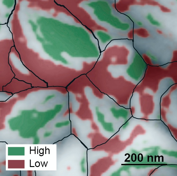
This atomic force microscopy image of the grainy surface of a perovskite solar cell reveals a new path to much greater efficiency. Individual grains are outlined in black, low-performing facets are red, and high-performing facets are green. A big jump in efficiency could possibly be obtained if the material can be grown so that more high-performing facets develop. (Credit: Berkeley Lab)
It’s always fascinating to observe a trend (or a craze) in science, an endeavour that outsiders (like me) tend to think of as impervious to such vagaries. Perovskite seems to be making its way past the trend/craze phase and moving into a more meaningful phase. From a July 4, 2016 news item on Nanowerk,
Scientists from the Department of Energy’s Lawrence Berkeley National Laboratory (Berkeley Lab) have discovered a possible secret to dramatically boosting the efficiency of perovskite solar cells hidden in the nanoscale peaks and valleys of the crystalline material.
Solar cells made from compounds that have the crystal structure of the mineral perovskite have captured scientists’ imaginations. They’re inexpensive and easy to fabricate, like organic solar cells. Even more intriguing, the efficiency at which perovskite solar cells convert photons to electricity has increased more rapidly than any other material to date, starting at three percent in 2009 — when researchers first began exploring the material’s photovoltaic capabilities — to 22 percent today. This is in the ballpark of the efficiency of silicon solar cells.
Now, as reported online July 4, 2016 in the journal Nature Energy (“Facet-dependent photovoltaic efficiency variations in single grains of hybrid halide perovskite”), a team of scientists from the Molecular Foundry and the Joint Center for Artificial Photosynthesis, both at Berkeley Lab, found a surprising characteristic of a perovskite solar cell that could be exploited for even higher efficiencies, possibly up to 31 percent.
A July 4, 2016 Berkeley Lab news release (also on EurekAlert), which originated the news item, details the research,
Using photoconductive atomic force microscopy, the scientists mapped two properties on the active layer of the solar cell that relate to its photovoltaic efficiency. The maps revealed a bumpy surface composed of grains about 200 nanometers in length, and each grain has multi-angled facets like the faces of a gemstone.
Unexpectedly, the scientists discovered a huge difference in energy conversion efficiency between facets on individual grains. They found poorly performing facets adjacent to highly efficient facets, with some facets approaching the material’s theoretical energy conversion limit of 31 percent.
The scientists say these top-performing facets could hold the secret to highly efficient solar cells, although more research is needed.
“If the material can be synthesized so that only very efficient facets develop, then we could see a big jump in the efficiency of perovskite solar cells, possibly approaching 31 percent,” says Sibel Leblebici, a postdoctoral researcher at the Molecular Foundry.
Leblebici works in the lab of Alexander Weber-Bargioni, who is a corresponding author of the paper that describes this research. Ian Sharp, also a corresponding author, is a Berkeley Lab scientist at the Joint Center for Artificial Photosynthesis. Other Berkeley Lab scientists who contributed include Linn Leppert, Francesca Toma, and Jeff Neaton, the director of the Molecular Foundry.
A team effort
The research started when Leblebici was searching for a new project. “I thought perovskites are the most exciting thing in solar right now, and I really wanted to see how they work at the nanoscale, which has not been widely studied,” she says.
She didn’t have to go far to find the material. For the past two years, scientists at the nearby Joint Center for Artificial Photosynthesis have been making thin films of perovskite-based compounds, and studying their ability to convert sunlight and CO2 into useful chemicals such as fuel. Switching gears, they created pervoskite solar cells composed of methylammonium lead iodide. They also analyzed the cells’ performance at the macroscale.
The scientists also made a second set of half cells that didn’t have an electrode layer. They packed eight of these cells on a thin film measuring one square centimeter. These films were analyzed at the Molecular Foundry, where researchers mapped the cells’ surface topography at a resolution of ten nanometers. They also mapped two properties that relate to the cells’ photovoltaic efficiency: photocurrent generation and open circuit voltage.
This was performed using a state-of-the-art atomic force microscopy technique, developed in collaboration with Park Systems, which utilizes a conductive tip to scan the material’s surface. The method also eliminates friction between the tip and the sample. This is important because the material is so rough and soft that friction can damage the tip and sample, and cause artifacts in the photocurrent.
Surprise discovery could lead to better solar cells
The resulting maps revealed an order of magnitude difference in photocurrent generation, and a 0.6-volt difference in open circuit voltage, between facets on the same grain. In addition, facets with high photocurrent generation had high open circuit voltage, and facets with low photocurrent generation had low open circuit voltage.
“This was a big surprise. It shows, for the first time, that perovskite solar cells exhibit facet-dependent photovoltaic efficiency,” says Weber-Bargioni.
Adds Toma, “These results open the door to exploring new ways to control the development of the material’s facets to dramatically increase efficiency.”
In practice, the facets behave like billions of tiny solar cells, all connected in parallel. As the scientists discovered, some cells operate extremely well and others very poorly. In this scenario, the current flows towards the bad cells, lowering the overall performance of the material. But if the material can be optimized so that only highly efficient facets interface with the electrode, the losses incurred by the poor facets would be eliminated.
“This means, at the macroscale, the material could possibly approach its theoretical energy conversion limit of 31 percent,” says Sharp.
A theoretical model that describes the experimental results predicts these facets should also impact the emission of light when used as an LED. …
The Molecular Foundry is a DOE Office of Science User Facility located at Berkeley Lab. The Joint Center for Artificial Photosynthesis is a DOE Energy Innovation Hub led by the California Institute of Technology in partnership with Berkeley Lab.
Here’s a link to and a citation for the paper,
Facet-dependent photovoltaic efficiency variations in single grains of hybrid halide perovskite by Sibel Y. Leblebici, Linn Leppert, Yanbo Li, Sebastian E. Reyes-Lillo, Sebastian Wickenburg, Ed Wong, Jiye Lee, Mauro Melli, Dominik Ziegler, Daniel K. Angell, D. Frank Ogletree, Paul D. Ashby, Francesca M. Toma, Jeffrey B. Neaton, Ian D. Sharp, & Alexander Weber-Bargioni. Nature Energy 1, Article number: 16093 (2016 doi:10.1038/nenergy.2016.93 Published online: 04 July 2016
This paper is behind a paywall.
Dexter Johnson’s July 6, 2016 posting on his Nanoclast blog (on the IEEE [Institute of Electrical and Electronics Engineers] website} presents his take on the impact that this new finding may have,
The rise of the crystal perovskite as a potential replacement for silicon in photovoltaics has been impressive over the last decade, with its conversion efficiency improving from 3.8 to 22.1 percent over that time period. Nonetheless, there has been a vague sense that this rise is beginning to peter out of late, largely because when a solar cell made from perovskite gets larger than 1 square centimeter the best conversion efficiency had been around 15.6 percent. …