Tag Archives: Jung-Hun Seo

Diamond-based electronics?

A May 24, 2016 news item on ScienceDaily describes the latest research on using diamonds as semiconductors,

Along with being a “girl’s best friend,” diamonds also have remarkable properties that could make them ideal semiconductors. This is welcome news for electronics; semiconductors are needed to meet the rising demand for more efficient electronics that deliver and convert power.

The thirst for electronics is unlikely to cease and almost every appliance or device requires a suite of electronics that transfer, convert and control power. Now, researchers have taken an important step toward that technology with a new way to dope single crystals of diamonds, a crucial process for building electronic devices.

A May 24, 2016 American Institute of Physics (AIP) news release (also on EurekAlert), which originated the news item, provides more detail,

For power electronics, diamonds could serve as the perfect material. They are thermally conductive, which means diamond-based devices would dissipate heat quickly and easily, foregoing the need for bulky and expensive methods for cooling. Diamond can also handle high voltages and power. Electrical currents also flow through diamonds quickly, meaning the material would make for energy efficient devices.

But among the biggest challenges to making diamond-based devices is doping, a process in which other elements are integrated into the semiconductor to change its properties. Because of diamond’s rigid crystalline structure, doping is difficult.

Currently, you can dope diamond by coating the crystal with boron and heating it to 1450 degrees Celsius. But it’s difficult to remove the boron coating at the end. This method only works on diamonds consisting of multiple crystals stuck together. Because such polydiamonds have irregularities between the crystals, single-crystals would be superior semiconductors.

You can dope single crystals by injecting boron atoms while growing the crystals artificially. The problem is the process requires powerful microwaves that can degrade the quality of the crystal.

Now, Ma [Zhengqiang (Jack) Ma, an electrical and computer engineering professor at the University of Wisconsin-Madison] and his colleagues have found a way to dope single-crystal diamonds with boron at relatively low temperatures and without any degradation. The researchers discovered if you bond a single-crystal diamond with a piece of silicon doped with boron, and heat it to 800 degrees Celsius, which is low compared to the conventional techniques, the boron atoms will migrate from the silicon to the diamond. It turns out that the boron-doped silicon has defects such as vacancies, where an atom is missing in the lattice structure. Carbon atoms from the diamond will fill those vacancies, leaving empty spots for boron atoms.

This technique also allows for selective doping, which means more control when making devices. You can choose where to dope a single-crystal diamond simply by bonding the silicon to that spot.

The new method only works for P-type doping, where the semiconductor is doped with an element that provides positive charge carriers (in this case, the absence of electrons, called holes).

“We feel like we found a very easy, inexpensive, and effective way to do it,” Ma said. The researchers are already working on a simple device using P-type single-crystal diamond semiconductors.

But to make electronic devices like transistors, you need N-type doping that gives the semiconductor negative charge carriers (electrons). And other barriers remain. Diamond is expensive and single crystals are very small.

Still, Ma says, achieving P-type doping is an important step, and might inspire others to find solutions for the remaining challenges. Eventually, he said, single-crystal diamond could be useful everywhere — perfect, for instance, for delivering power through the grid.

Here’s an image the researchers have released,
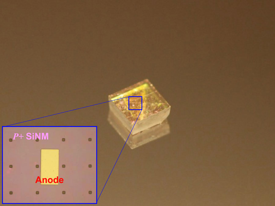
Optical image of a diode array on a natural single crystalline diamond plate. (The image looks blurred due to light scattering by the array of small pads on top of the diamond plate.) Inset shows the deposited anode metal on top of heavy doped Si nanomembrane that is bonded to natural single crystalline diamond. CREDIT: Jung-Hun Seo

Optical image of a diode array on a natural single crystalline diamond plate. (The image looks blurred due to light scattering by the array of small pads on top of the diamond plate.) Inset shows the deposited anode metal on top of heavy doped Si nanomembrane that is bonded to natural single crystalline diamond. CREDIT: Jung-Hun Seo Courtesy: American Institute of Physics

Here’s a link to and a citation for the paper,

Thermal diffusion boron doping of single-crystal natural diamond by Jung-Hun Seo, Henry Wu, Solomon Mikael, Hongyi Mi, James P. Blanchard, Giri Venkataramanan, Weidong Zhou, Shaoqin Gong, Dane Morgan, and Zhenqiang Ma. J. Appl. Phys. 119, 205703 (2016); http://dx.doi.org/10.1063/1.4949327

This paper appears to be open access.

Cellulose Nanofibrillated Fiber Based Transistors from the University of Wisconsin-Madison

There’s a team of researchers at the University of Wisconsin-Madison working to substitute silicon used in computer chips with cellulose derived from wood (my May 27, 2015 posting). Their latest effort, featuring mobile electronics, is described in a July 1, 2015 news item on Azonano,

A report published by the U.S. Environmental Protection Agency in 2012 showed that about 152 million mobile devices are discarded every year, of which only 10 percent is recycled — a legacy of waste that consumes a tremendous amount of natural resources and produces a lot of trash made from expensive and non-biodegradable materials like highly purified silicon.

Now researchers from the University of Wisconsin-Madison have come up with a new solution to alleviate the environmental burden of discarded electronics. They have demonstrated the feasibility of making microwave biodegradable thin-film transistors from a transparent, flexible biodegradable substrate made from inexpensive wood, called cellulose nanofibrillated fiber (CNF). This work opens the door for green, low-cost, portable electronic devices in future.

A June 30, 2015 American Institute of Physics news release by Zhengzheng Zhang, which originated the news item, describes the research in more detail,

“We found that cellulose nanofibrillated fiber based transistors exhibit superior performance as that of conventional silicon-based transistors,” said Zhenqiang Ma, the team leader and a professor of electrical and computer engineering at the UW-Madison. “And the bio-based transistors are so safe that you can put them in the forest, and fungus will quickly degrade them. They become as safe as fertilizer.”

Nowadays, the majority of portable electronics are built on non-renewable, non-biodegradable materials such as silicon wafers, which are highly purified, expensive and rigid substrates, but cellulose nanofibrillated fiber films have the potential to replace silicon wafers as electronic substrates in environmental friendly, low-cost, portable gadgets or devices of the future.

Cellulose nanofibrillated fiber is a sustainable, strong, transparent nanomaterial made from wood. Compared to other polymers like plastics, the wood nanomaterial is biocompatible and has relatively low thermal expansion coefficient, which means the material won’t change shape as the temperature changes. All these superior properties make cellulose nanofibril an outstanding candidate for making portable green electronics.

To create high-performance devices, Ma’s team employed silicon nanomembranes as the active material in the transistor — pieces of ultra-thin films (thinner than a human hair) peeled from the bulk crystal and then transferred and glued onto the cellulose nanofibrill substrate to create a flexible, biodegradable and transparent silicon transistor.To create high-performance devices, Ma’s team employed silicon nanomembranes as the active material in the transistor — pieces of ultra-thin films (thinner than a human hair) peeled from the bulk crystal and then transferred and glued onto the cellulose nanofibrill substrate to create a flexible, biodegradable and transparent silicon transistor.

But to make portable electronics, the biodegradable transistor needed to be able to operate at microwave frequencies, which is the working range of most wireless devices. The researchers thus conducted a series of experiments such as measuring the current-voltage characteristics to study the device’s functional performance, which finally showed the biodegradable transistor has superior microwave-frequency operation capabilities comparable to existing semiconductor transistors.

“Biodegradable electronics provide a new solution for environmental problems brought by consumers’ pursuit of quickly upgraded portable devices,” said Ma. “It can be anticipated that future electronic chips and portable devices will be much greener and cheaper than that of today.”

Next, Ma and colleagues plan to develop more complicated circuit system based on the biodegradable transistors.

Here’s a link to and a citation for the team’s latest paper,

Microwave flexible transistors on cellulose nanofibrillated fiber substrates by Jung-Hun Seo, Tzu-Hsuan Chang, Jaeseong Lee, Ronald Sabo, Weidong Zhou, Zhiyong Cai, Shaoqin Gong, and Zhenqiang Ma.  Applied Physics Letters, Volume 106, Issue 26 or  Appl. Phys. Lett. 106, 262101 (2015); http://dx.doi.org/10.1063/1.4921077

This is an open access paper.