Tag Archives: Kazu Suenaga

Unraveling carbyne (one-dimensional carbon)

An international group of researchers has developed a technique for producing a record-breaking length of one-dimensional carbon (carbon chain) according to an April 4, 2016 news item on Nanowerk,

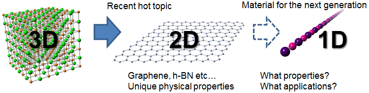
Elemental carbon appears in many different modifications, including diamond, fullerenes and graphene. Their unique structural, electronic, mechanical, transport and optical properties have a broad range of applications in physics, chemistry and materials science, including composite materials, nanoscale light emitting devices and energy harvesting materials. Within the “carbon family”, only carbyne, the truly one-dimensional form of carbon, has not yet been synthesized despite having been studied for more than 50 years. Its extreme instability in ambient conditions rendered the final experimental proof of its existence elusive.

An international collaboration of researchers now succeeded in developing a novel route for the bulk production of carbon chains composed of more than 6,400 carbon atoms by using thin double-walled carbon nanotubes as protective hosts for the chains.

An April 4, 2016 University of Vienna press release (also on EurekAlert) provides another perspective on the research,

Even in its elemental form, the high bond versatility of carbon allows for many different well-known materials, including diamond and graphite. A single layer of graphite, termed graphene, can then be rolled or folded into carbon nanotubes or fullerenes, respectively. To date, Nobel prizes have been awarded for both graphene (2010) and fullerenes (1996). Although the existence of carbyne, an infinitely long carbon chain, was proposed in 1885 by Adolf von Baeyer (Nobel laureate for his overall contributions in organic chemistry, 1905), scientists have not yet been able to synthesize this material. Von Baeyer even suggested that carbyne would remain elusive as its high reactivity would always lead to its immediate destruction. Nevertheless, carbon chains of increasing length have been successfully synthesized over the last 50 years, with a record of around 100 carbon atoms (2003). This record has now been broken by more than one order of magnitude, with the demonstration of micrometer length-scale chains.

The new record

Researchers from the University of Vienna, led by Thomas Pichler, have presented a novel approach to grow and stabilize carbon chains with a record length of 6,000 carbon atoms, improving the previous record by more than one order of magnitude. They use the confined space inside a double-walled carbon nanotube as a nano-reactor to grow ultra-long carbon chains on a bulk scale. In collaboration with the groups of Kazu Suenaga at the AIST Tsukuba [National Institute of Advanced Industrial Science and Technology] in Japan, Lukas Novotny at the ETH Zürich [Swiss Federal Institute of Technology] in Switzerland and Angel Rubio at the MPI [Max Planck Institute] Hamburg in Germany and UPV/EHU [University of the Basque Country] San Sebastian in Spain, the existence of the chains has been unambiguously confirmed by using a multitude of sophisticated, complementary methods. These are temperature dependent near- and far-field Raman spectroscopy with different lasers (for the investigation of electronic and vibrational properties), high resolution transmission electron spectroscopy (for the direct observation of carbyne inside the carbon nanotubes) and x-ray scattering (for the confirmation of bulk chain growth).

The researchers present their study in the latest edition of Nature Materials. “The direct experimental proof of confined ultra-long linear carbon chains, which are more than an order of magnitude longer than the longest proven chains so far, can be seen as a promising step towards the final goal of unraveling the “holy grail” of carbon allotropes, carbyne”, explains the lead author, Lei Shi.

Application potential

Carbyne is very stable inside double-walled carbon nanotubes. This property is crucial for its eventual application in future materials and devices. According to theoretical models, carbyne’s mechanical properties exceed all known materials, outperforming both graphene and diamond. Carbyne’s electrical properties suggest novel nanoelectronic applications in quantum spin transport and magnetic semiconductors.

Here’s a link to and a citation for the paper,

Confined linear carbon chains as a route to bulk carbyne by Lei Shi, Philip Rohringer, Kazu Suenaga, Yoshiko Niimi, Jani Kotakoski, Jannik C. Meyer, Herwig Peterlik, Marius Wanko, Seymur Cahangirov, Angel Rubio, Zachary J. Lapin, Lukas Novotny, Paola Ayala, & Thomas Pichler. Nature Materials (2016) doi:10.1038/nmat4617 Published online 04 April 2016

This paper is behind a paywall.

But, there is this earlier and open access version on arXiv.org,

Confined linear carbon chains: A route to bulk carbyne
Lei Shi, Philip Rohringer, Kazu Suenaga, Yoshiko Niimi, Jani Kotakoski, Jannik C. Meyer, Herwig Peterlik, Paola Ayala, Thomas Pichler (Submitted on 17 Jul 2015 (v1), last revised 20 Jul 2015 (this version, v2))

Nestling a two-element atomic chain inside a carbon nanotube

While there doesn’t seem to be a short-term application for this research from Japan, the idea of nestling a chain of two elements inside a carbon nanotube is intriguing, from an Oct. 16, 2014 news item on Nanowerk,

Kazutomo Suenaga of the Nanotube Research Center (NTRC) of the National Institute of Advanced Industrial Science and Technology (AIST) and Ryosuke Senga of the Nano-carbon Characterization Team, NTRC, AIST, have synthesized an atomic chain in which two elements are aligned alternately and have evaluated its physical properties on an atomic level.

An ionic crystalline atomic chain of cesium iodine (CsI) has been synthesized by aligning a cesium ion (Cs+), a cation and an iodine ion (I-), an anion, alternately by encapsulating CsI in the microscopic space inside a carbon nanotube. Furthermore, by using an advanced aberration-corrected electron microscope, the physical phenomena unique to the CsI atomic chain, such as the difference in dynamic behavior of its cations and anions, have been discovered. In addition, from theoretical calculation using density functional theory (DFT), this CsI atomic chain has been found to indicate different optical properties from a three-dimensional CsI crystal, and applications to new optical devices are anticipated.

An Oct. 16, 2014 National Institute of Advanced Industrial Science and Technology (AIST) press release, which originated the news item, situates the research within a social and historical context,

Social Background of Research

In the accelerating and ballooning information society, electronic devices used in computers and smartphones has constantly demanded higher performance and efficiency. The materials currently drawing expectations are low-dimensional materials with a single to few-atom width and thickness. Two-dimensional materials, typified by graphene, indicate unique physical characteristics not found in three-dimensional materials, such as its excellent electrical transport properties, and are being extensively researched.

An atomic chain, which has an even finer structure with a width of only one atom, has been predicted to display excellent electrical transport properties, like two-dimensional materials. Although expectations were higher than for two-dimensional materials from the viewpoint of integration, it had attracted little attention until now. This is because of the technological difficulties faced by the various processes of academic research from synthesis to analysis of atomic chains, and academic understanding has not progressed far (Fig. 1).

Figure 1
Figure 1 : Transition of target materials in material research

History of Research

AIST has been developing element analysis methods on a single-atom level to detect certain special structures including impurities, dopants and defects, that affect the properties of low-dimensional materials such as carbon nanotubes and graphene (AIST press releases on July 6, 2009, January 12, 2010, December 16, 2010 and July 9, 2012). In this research, efforts were made for the synthesis and analysis of the atomic chain, a low-dimensional material, using the accumulated technological expertise. This research has been supported by both the Strategic Basic Research Program of the Japan Science and Technology Agency (FY2012 to FY2016), and the Grants-in-aid for Scientific Research of the Japan Society for the Promotion of Science, “Development of elemental technology for the atomic-scale evaluation and application of low-dimensional materials using nano-space” (FY2014 to FY2016).

The press release also offers more details about the research and future applications,

Details of Research

The developed technology is the technology to expose carbon nanotubes, with a diameter of 1 nm or smaller, to CsI vapor to encapsulate CsI in the microscopic space inside the carbon nanotubes, to synthesize an atomic chain in which two elements, Cs and I, are aligned alternately. Furthermore, by combining aberration-corrected electron microscopy and an electronic spectroscopic technique known as electron energy-loss spectroscopy (EELS) detailed structural analysis of this atomic chain was conducted. In order to identify each atom aligned at a distance of 1 nm or less without destroying them, the accelerating voltage of the electron microscope was significantly lowered to 60 kV to reduce damage to the sample by electron beams, while maintaining sufficient spatial resolution of around 1 nm. Figure 2 indicates the smallest CsI crystal confirmed so far, and the CsI atomic chain synthesized in this research.

Figure 2
Figure 2 : Comparison of CsI atomic chain and CsI crystal
(Top: Actual annular dark-field images, Bottom: Corresponding models)

Figure 3 shows the annular dark-field (ADF) image of the CsI atomic chain and the element mapping for Cs and I, respectively, obtained by EELS. It can be seen that the two elements are aligned alternately. There has not been any report of this simple and ideal structure actually being produced and observed, and it can be said to be a fundamental, important finding in material science.

Normally, in an ADF image, those with larger atomic numbers appear brighter. However, in this CsI atomic chain, I (atomic number 53) appears brighter than Cs (atomic number 55). This is because Cs, being a cation, moves more actively (more accurately, the total amount of electrons scattered by the Cs atom is not very different from those of the I atom, but the electrons scattered by the moving Cs atom generate spatial expansion), indicating a difference in dynamic behavior of the cation and the anion that cannot occur in a large three-dimensional crystal. Locations where single Cs atom or I atom is absent, namely vacancies, were also found (Fig. 3, right).

The unique behavior and structure influence various physical properties. When optical absorption spectra were calculated using DFT, the response of the CsI atomic chain to light differed with the direction of incidence. Furthermore, it was found that in a CsI atomic chain with vacancies, the electron state of vacancy sites where the I atom is absent possess a donor level at which electrons were easily released, while vacancy sites where the Cs atom is absent possess a receptor level at which electrons were easily received. By making use of these physical properties, applications to new electro-optical devices, such as a micro-light source and an optical switch using light emission from a single vacancy in the CsI atomic chain, are conceivable. In addition, further research into combinations of other elements triggered by the present results may lead to the development of new materials and device applications. There are expectations for atomic chains to be the next-generation materials for devices in search of further miniaturization and integration.

Figure 3
Figure 3 : Synthesized CsI atomic chain, encapsulated in double-walled carbon nanotube
(From left: ADF image, element maps for Cs and I, model, ADF image of CsI atomic chains with vacancies)

Future Plans

Since the CsI atomic chain displays optical properties significantly different from large crystals that can be seen by the human eye, there are expectations for its application for new electro-optical devices such as a micro-light source and an optical switch using light emission from a single vacancy in the CsI atomic chain. The researchers will conduct experimental research in its application, focused on detailed study of its various physical properties, starting with its optical properties. In addition to CsI, efforts will also be made in the development of new materials that combine various elements, by applying this technology to other materials.

Furthermore, the mechanism of all adsorbents of radioactive substances (carbon nanotubes, zeolite, Prussian blue, etc.) currently being developed for commercial use are methods of encapsulating radioactive atoms inside microscopic space in the material. The researchers hope to utilize the knowledge of the behavior of the Cs atom in a microscopic space obtained in this research, to improve adsorption performance.

Here’s a link to and a citation for the research paper,

Atomic structure and dynamic behaviour of truly one-dimensional ionic chains inside ​carbon nanotubes by Ryosuke Senga, Hannu-Pekka Komsa, Zheng Liu, Kaori Hirose-Takai, Arkady V. Krasheninnikov, & Kazu Suenaga. Nature Materials (2014) doi:10.1038/nmat4069 Published online 14 September 2014

This paper is behind a paywall.