Tag Archives: Kojiro Uetani

Growing electronics on trees

An April 26, 2022 news item on phys.org caught my eye with its mention of nanocellulose, trees, and electronics,

Electronics can grow on trees thanks to nanocellulose paper semiconductors

Semiconducting nanomaterials with 3D network structures have high surface areas and a lot of pores that make them excellent for applications involving adsorbing, separating, and sensing. However, simultaneously controlling the electrical properties and creating useful micro- and macro-scale structures, while achieving excellent functionality and end-use versatility, remains challenging. Now, Osaka University researchers, in collaboration with The University of Tokyo, Kyushu University, and Okayama University, have developed a nanocellulose paper semiconductor that provides both nano−micro−macro trans-scale designability of the 3D structures and wide tunability of the electrical properties. Their findings are published in ACS Nano.

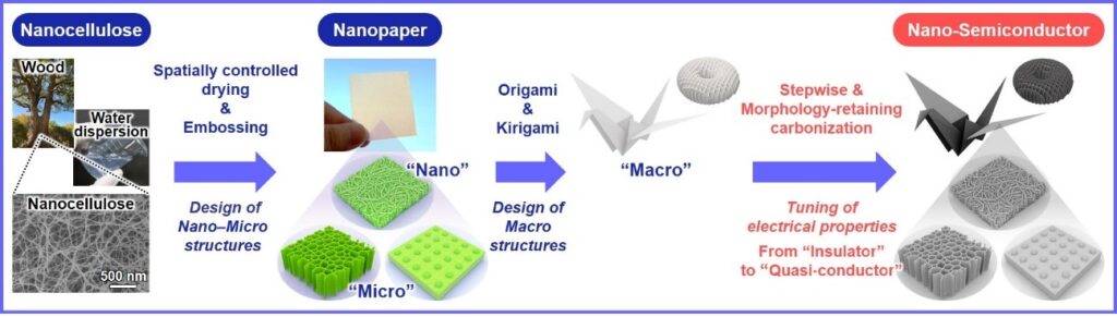
Cellulose is a natural and easy to source material derived from wood. Cellulose nanofibers (nanocellulose) can be made into sheets of flexible nanocellulose paper (nanopaper) with dimensions like those of standard A4. Nanopaper does not conduct an electric current; however, heating can introduce conducting properties. Unfortunately, this exposure to heat can also disrupt the nanostructure.

The researchers have therefore devised a treatment process that allows them to heat the nanopaper without damaging the structures of the paper from the nanoscale up to the macroscale.

Caption: Schematic diagram of the preparation of the wood nanocellulose-derived nano-semiconductor with customizable electrical properties and 3D structures Credit: 2022 Koga et al. Nanocellulose paper semiconductor with a 3D network structure and its nano−micro−macro trans-scale design. ACS Nano

An April 28, 2022 Osaka University news release (also on EurekAlert), which originated the news item, provides more detail about the work

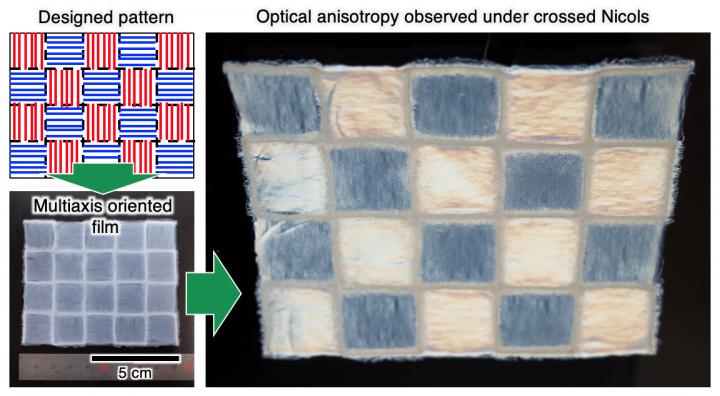
“An important property for the nanopaper semiconductor is tunability because this allows devices to be designed for specific applications,” explains study author Hirotaka Koga. “We applied an iodine treatment that was very effective for protecting the nanostructure of the nanopaper. Combining this with spatially controlled drying meant that the pyrolysis treatment did not substantially alter the designed structures and the selected temperature could be used to control the electrical properties.”

The researchers used origami (paper folding) and kirigami (paper cutting) techniques to provide playful examples of the flexibility of the nanopaper at the macrolevel. A bird and box were folded, shapes including an apple and snowflake were punched out, and more intricate structures were produced by laser cutting. This demonstrated the level of detail possible, as well as the lack of damage caused by the heat treatment.

Examples of successful applications showed nanopaper semiconductor sensors incorporated into wearable devices to detect exhaled moisture breaking through facemasks and moisture on the skin. The nanopaper semiconductor was also used as an electrode in a glucose biofuel cell and the energy generated lit a small bulb.

“The structure maintenance and tunability that we have been able to show is very encouraging for the translation of nanomaterials into practical devices,” says Associate Professor Koga. “We believe that our approach will underpin the next steps in sustainable electronics made entirely from plant materials.”

About Osaka University

Osaka University was founded in 1931 as one of the seven imperial universities of Japan and is now one of Japan’s leading comprehensive universities with a broad disciplinary spectrum. This strength is coupled with a singular drive for innovation that extends throughout the scientific process, from fundamental research to the creation of applied technology with positive economic impacts. Its commitment to innovation has been recognized in Japan and around the world, being named Japan’s most innovative university in 2015 (Reuters 2015 Top 100) and one of the most innovative institutions in the world in 2017 (Innovative Universities and the Nature Index Innovation 2017). Now, Osaka University is leveraging its role as a Designated National University Corporation selected by the Ministry of Education, Culture, Sports, Science and Technology to contribute to innovation for human welfare, sustainable development of society, and social transformation.

Here’s a link to and a citation for the paper,

Nanocellulose Paper Semiconductor with a 3D Network Structure and Its Nano–Micro–Macro Trans-Scale Design by Hirotaka Koga, Kazuki Nagashima, Koichi Suematsu, Tsunaki Takahashi, Luting Zhu, Daiki Fukushima, Yintong Huang, Ryo Nakagawa, Jiangyang Liu, Kojiro Uetani, Masaya Nogi, Takeshi Yanagida, and Yuta Nishina. ACS Nano 2022, XXXX, XXX, XXX-XXX DOI: https://doi.org/10.1021/acsnano.1c10728 Publication Date:April 26, 2022 © 2022 The Authors. Published by American Chemical Society

The paper appears to be open access.

Nanocellulose films made with liquid-phase fabrication method

I always appreciate a reference to Star Trek and three-dimensional chess was one of my favourite concepts. You’ll find that and more in a May 19, 2020 news item on Nanowerk,

Researchers at The Institute of Scientific and Industrial Research at Osaka University [Japan] introduced a new liquid-phase fabrication method for producing nanocellulose films with multiple axes of alignment. Using 3D-printing methods for increased control, this work may lead to cheaper and more environmentally friendly optical and thermal devices.

Ever since appearing on the original Star Trek TV show in the 1960s, the game of “three-dimensional chess” has been used as a metaphor for sophisticated thinking. Now, researchers at Osaka University can say that they have added their own version, with potential applications in advanced optics and inexpensive smartphone displays.

It’s not exactly three-dimensional chess but this nanocellulose film was produced by 3D printing methods,

Caption: Developed multiaxis nanocellulose-oriented film. Credit: Osaka University

A May 20, 2020 Osaka University press release (also on EurekAlert but dated May 19, 2020), which originated the news item, provides more detail,

Many existing optical devices, including liquid-crystal displays (LCDs) found in older flat-screen televisions, rely on long needle-shaped molecules aligned in the same direction. However, getting fibers to line up in multiple directions on the same device is much more difficult. Having a method that can reliably and cheaply produce optical fibers would accelerate the manufacture of low-cost displays or even “paper electronics”–computers that could be printed from biodegradable materials on demand.

Cellulose, the primary component of cotton and wood, is an abundant renewable resource made of long molecules. Nanocelluloses are nanofibers made of uniaxially aligned cellulose molecular chains that have different optical and heat conduction properties along one direction compared to the another.

In newly published research from the Institute of Scientific and Industrial Research at Osaka University, nanocellulose was harvested from sea pineapples, a kind of sea squirt. They then used liquid-phase 3D-pattering, which combined the wet spinning of nanofibers with the precision of 3D-printing. A custom-made triaxial robot dispensed a nanocellulose aqueous suspension into an acetone coagulation bath.

“We developed this liquid-phase three-dimensional patterning technique to allow for nanocellulose alignment along any preferred axis,” says first author Kojiro Uetani. The direction of the patterns could be programmed so that it formed an alternating checkerboard pattern of vertically- and horizontally-aligned fibers.

To demonstrate the method, a film was sandwiched between two orthogonal polarizing films. Under the proper viewing conditions, a birefringent checkerboard pattern appeared. They also measured the thermal transfer and optical retardation properties.

“Our findings could aid in the development of next-generation optical materials and paper electronics,” says senior author Masaya Nogi. “This could be the start of bottom-up techniques for building sophisticated and energy-efficient optical and thermal materials.”

Here’s a link to and a citation for the paper,

Checkered Films of Multiaxis Oriented Nanocelluloses by Liquid-Phase Three-Dimensional Patterning by Kojiro Uetani, Hirotaka Koga and Masaya Nogi. Nanomaterials 2020, 10(5), 958; DOI: https://doi.org/10.3390/nano10050958 Published: 18 May 2020

This is an open access paper.

Dessert or computer screen?

Scientists at Japan’s University of Osaka have a technique for creating higher resolution computer and smart phone screens from the main ingredient for a dessert, nata de coco. From the nata de coco Wikipedia entry (Note: Links have been removed),

Nata de coco (also marketed as “coconut gel”) is a chewy, translucent, jelly-like food produced by the fermentation of coconut water,[1] which gels through the production of microbial cellulose by ‘Komagataeibacter xylinus’. Originating in the Philippines, nata de coco is most commonly sweetened as a candy or dessert, and can accompany a variety of foods, including pickles, drinks, ice cream, puddings, and fruit cocktails.[2]

An April 18, 2018 news item on Nanowerk announces the research (Note: A link has been removed),

A team at the Institute of Scientific and Industrial Research at Osaka University has determined the optical parameters of cellulose molecules with unprecedented precision. They found that cellulose’s intrinsic birefringence, which describes how a material reacts differently to light of various orientations, is powerful enough to be used in optical displays, such as flexible screens or electronic paper (ACS Macro Letters, “Estimation of the Intrinsic Birefringence of Cellulose Using Bacterial Cellulose Nanofiber Films”

An April 18, 2019 Osaka University press release on AlphaGalileo, which originated the news release, provides some historical context for the use of cellulose along with additional detail about the research,

Cellulose is an ancient material that may be poised for a major comeback. It has been utilized for millennia as the primary component of paper books, cotton clothing, and nata de coco, a tropical dessert made from coconut water. While books made of dead trees and plain old shirts might seem passé in world increasingly filled with tablets and smartphones, researchers at Osaka University have shown that cellulose might have just what it takes to make our modern electronic screens cheaper and provide sharper, more vibrant images.

Cellulose, a naturally occurring polymer, consists of many long molecular chains. Because of its rigidity and strength, cellulose helps maintain the structural integrity of the cell walls in plants. It makes up about 99% of the nanofibers that comprise nata de coco, and helps create its unique and tasty texture.

The team at Osaka University achieved better results using unidirectionally-aligned cellulose nanofiber films created by stretching hydrogels from nata de coco at various rates. Nata de coco nanofibers allow the cellulose chains to be straight on the molecular level, and this is helpful for the precise determination of the intrinsic birefringence–that is, the maximum birefringence of fully extended polymer chains. The researchers were also able to measure the birefringence more accurately through improvements in method. “Using high quality samples and methods, we were able to reliably determine the inherent birefringence of cellulose, for which very different values had been previously estimated,” says senior author Masaya Nogi.

The main application the researchers envision is as light compensation films for liquid crystal displays (LCDs), since they operate by controlling the brightness of pixels with filters that allow only one orientation of light to pass through. Potentially, any smartphone, computer, or television that has an LCD screen could see improved contrast, along with reduced color unevenness and light leakage with the addition of cellulose nanofiber films.

“Cellulose nanofibers are promising light compensation materials for optoelectronics, such as flexible displays and electronic paper, since they simultaneously have good transparency, flexibility, dimensional stability, and thermal conductivity,” says lead author Kojiro Uetani. “So look for this ancient material in your future high-tech devices.”

Here’s a link to and a citation for the paper,

Estimation of the Intrinsic Birefringence of Cellulose Using Bacterial Cellulose Nanofiber Films by Kojiro Uetani, Hirotaka Koga, and Masaya Nogi. ACS Macro Lett., 2019, 8 (3), pp 250–254 DOI: 10.1021/acsmacrolett.9b00024 Publication Date (Web): February 22, 2019 Copyright © 2019 American Chemical Society

This paper is behind a paywall.