Tag Archives: LBNL

3D printed all liquid electronics

Even after watching the video, I still don’t quite believe it. A March 28, 2018 news item on ScienceDaily announces the work,

Scientists from the Department of Energy’s Lawrence Berkeley National Laboratory (Berkeley Lab [or LBNL]) have developed a way to print 3-D structures composed entirely of liquids. Using a modified 3-D printer, they injected threads of water into silicone oil — sculpting tubes made of one liquid within another liquid.

They envision their all-liquid material could be used to construct liquid electronics that power flexible, stretchable devices. The scientists also foresee chemically tuning the tubes and flowing molecules through them, leading to new ways to separate molecules or precisely deliver nanoscale building blocks to under-construction compounds.

A March 28, 2018 Berkeley Lab March 26, 2018 news release (also on EurekAlert), which originated the news item, describe the work in more detail,

The researchers have printed threads of water between 10 microns and 1 millimeter in diameter, and in a variety of spiraling and branching shapes up to several meters in length. What’s more, the material can conform to its surroundings and repeatedly change shape.

“It’s a new class of material that can reconfigure itself, and it has the potential to be customized into liquid reaction vessels for many uses, from chemical synthesis to ion transport to catalysis,” said Tom Russell, a visiting faculty scientist in Berkeley Lab’s Materials Sciences Division. He developed the material with Joe Forth, a postdoctoral researcher in the Materials Sciences Division, as well as other scientists from Berkeley Lab and several other institutions. They report their research March 24 [2018] in the journal Advanced Materials.

The material owes its origins to two advances: learning how to create liquid tubes inside another liquid, and then automating the process.

For the first step, the scientists developed a way to sheathe tubes of water in a special nanoparticle-derived surfactant that locks the water in place. The surfactant, essentially soap, prevents the tubes from breaking up into droplets. Their surfactant is so good at its job, the scientists call it a nanoparticle supersoap.

The supersoap was achieved by dispersing gold nanoparticles into water and polymer ligands into oil. The gold nanoparticles and polymer ligands want to attach to each other, but they also want to remain in their respective water and oil mediums. The ligands were developed with help from Brett Helms at the Molecular Foundry, a DOE Office of Science User Facility located at Berkeley Lab.

In practice, soon after the water is injected into the oil, dozens of ligands in the oil attach to individual nanoparticles in the water, forming a nanoparticle supersoap. These supersoaps jam together and vitrify, like glass, which stabilizes the interface between oil and water and locks the liquid structures in position.

This stability means we can stretch water into a tube, and it remains a tube. Or we can shape water into an ellipsoid, and it remains an ellipsoid,” said Russell. “We’ve used these nanoparticle supersoaps to print tubes of water that last for several months.”

Next came automation. Forth modified an off-the-shelf 3-D printer by removing the components designed to print plastic and replacing them with a syringe pump and needle that extrudes liquid. He then programmed the printer to insert the needle into the oil substrate and inject water in a predetermined pattern.

“We can squeeze liquid from a needle, and place threads of water anywhere we want in three dimensions,” said Forth. “We can also ping the material with an external force, which momentarily breaks the supersoap’s stability and changes the shape of the water threads. The structures are endlessly reconfigurable.”

This image illustrates how the water is printed,

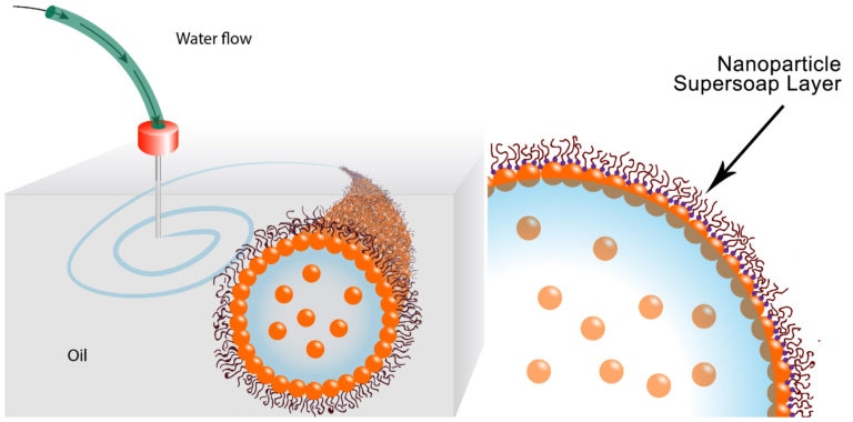
These schematics show the printing of water in oil using a nanoparticle supersoap. Gold nanoparticles in the water combine with polymer ligands in the oil to form an elastic film (nanoparticle supersoap) at the interface, locking the structure in place. (Credit: Berkeley Lab)

Here’s a link to and a citation for the paper,

Reconfigurable Printed Liquids by Joe Forth, Xubo Liu, Jaffar Hasnain, Anju Toor, Karol Miszta, Shaowei Shi, Phillip L. Geissler, Todd Emrick, Brett A. Helms, Thomas P. Russell. Advanced Materials https://doi.org/10.1002/adma.201707603 First published: 24 March 2018

This paper is behind a paywall.

X-rays reveal memristor workings

A June 14, 2016 news item on ScienceDaily focuses on memristors. (It’s been about two months since my last memristor posting on April 22, 2016 regarding electronic synapses and neural networks). This piece announces new insight into how memristors function at the atomic scale,

In experiments at two Department of Energy national labs — SLAC National Accelerator Laboratory and Lawrence Berkeley National Laboratory — scientists at Hewlett Packard Enterprise (HPE) [also referred to as HP Labs or Hewlett Packard Laboratories] have experimentally confirmed critical aspects of how a new type of microelectronic device, the memristor, works at an atomic scale.

This result is an important step in designing these solid-state devices for use in future computer memories that operate much faster, last longer and use less energy than today’s flash memory. …

“We need information like this to be able to design memristors that will succeed commercially,” said Suhas Kumar, an HPE scientist and first author on the group’s technical paper.

A June 13, 2016 SLAC news release, which originated the news item, offers a brief history according to HPE and provides details about the latest work,

The memristor was proposed theoretically [by Dr. Leon Chua] in 1971 as the fourth basic electrical device element alongside the resistor, capacitor and inductor. At its heart is a tiny piece of a transition metal oxide sandwiched between two electrodes. Applying a positive or negative voltage pulse dramatically increases or decreases the memristor’s electrical resistance. This behavior makes it suitable for use as a “non-volatile” computer memory that, like flash memory, can retain its state without being refreshed with additional power.

Over the past decade, an HPE group led by senior fellow R. Stanley Williams has explored memristor designs, materials and behavior in detail. Since 2009 they have used intense synchrotron X-rays to reveal the movements of atoms in memristors during switching. Despite advances in understanding the nature of this switching, critical details that would be important in designing commercially successful circuits  remained controversial. For example, the forces that move the atoms, resulting in dramatic resistance changes during switching, remain under debate.

In recent years, the group examined memristors made with oxides of titanium, tantalum and vanadium. Initial experiments revealed that switching in the tantalum oxide devices could be controlled most easily, so it was chosen for further exploration at two DOE Office of Science User Facilities – SLAC’s Stanford Synchrotron Radiation Lightsource (SSRL) and Berkeley Lab’s Advanced Light Source (ALS).

At ALS, the HPE researchers mapped the positions of oxygen atoms before and after switching. For this, they used a scanning transmission X-ray microscope and an apparatus they built to precisely control the position of their sample and the timing and intensity of the 500-electronvolt ALS X-rays, which were tuned to see oxygen.

The experiments revealed that even weak voltage pulses create a thin conductive path through the memristor. During the pulse the path heats up, which creates a force that pushes oxygen atoms away from the path, making it even more conductive. Reversing the voltage pulse resets the memristor by sucking some of oxygen atoms back into the conducting path, thereby increasing the device’s resistance. The memristor’s resistance changes between 10-fold and 1 million-fold, depending on operating parameters like the voltage-pulse amplitude. This resistance change is dramatic enough to exploit commercially.

To be sure of their conclusion, the researchers also needed to understand if the tantalum atoms were moving along with the oxygen during switching. Imaging tantalum required higher-energy, 10,000-electronvolt X-rays, which they obtained at SSRL’s Beam Line 6-2. In a single session there, they determined that the tantalum remained stationary.

“That sealed the deal, convincing us that our hypothesis was correct,” said HPE scientist Catherine Graves, who had worked at SSRL as a Stanford graduate student. She added that discussions with SLAC experts were critical in guiding the HPE team toward the X-ray techniques that would allow them to see the tantalum accurately.

Kumar said the most promising aspect of the tantalum oxide results was that the scientists saw no degradation in switching over more than a billion voltage pulses of a magnitude suitable for commercial use. He added that this knowledge helped his group build memristors that lasted nearly a billion switching cycles, about a thousand-fold improvement.

“This is much longer endurance than is possible with today’s flash memory devices,” Kumar said. “In addition, we also used much higher voltage pulses to accelerate and observe memristor failures, which is also important in understanding how these devices work. Failures occurred when oxygen atoms were forced so far away that they did not return to their initial positions.”

Beyond memory chips, Kumar says memristors’ rapid switching speed and small size could make them suitable for use in logic circuits. Additional memristor characteristics may also be beneficial in the emerging class of brain-inspired neuromorphic computing circuits.

“Transistors are big and bulky compared to memristors,” he said. “Memristors are also much better suited for creating the neuron-like voltage spikes that characterize neuromorphic circuits.”

The researchers have provided an animation illustrating how memristors can fail,

This animation shows how millions of high-voltage switching cycles can cause memristors to fail. The high-voltage switching eventually creates regions that are permanently rich (blue pits) or deficient (red peaks) in oxygen and cannot be switched back. Switching at lower voltages that would be suitable for commercial devices did not show this performance degradation. These observations allowed the researchers to develop materials processing and operating conditions that improved the memristors’ endurance by nearly a thousand times. (Suhas Kumar) Courtesy: SLAC

This animation shows how millions of high-voltage switching cycles can cause memristors to fail. The high-voltage switching eventually creates regions that are permanently rich (blue pits) or deficient (red peaks) in oxygen and cannot be switched back. Switching at lower voltages that would be suitable for commercial devices did not show this performance degradation. These observations allowed the researchers to develop materials processing and operating conditions that improved the memristors’ endurance by nearly a thousand times. (Suhas Kumar) Courtesy: SLAC

Here’s a link to and a citation for the paper,

Direct Observation of Localized Radial Oxygen Migration in Functioning Tantalum Oxide Memristors by Suhas Kumar, Catherine E. Graves, John Paul Strachan, Emmanuelle Merced Grafals, Arthur L. David Kilcoyne3, Tolek Tyliszczak, Johanna Nelson Weker, Yoshio Nishi, and R. Stanley Williams. Advanced Materials, First published: 2 February 2016; Print: Volume 28, Issue 14 April 13, 2016 Pages 2772–2776 DOI: 10.1002/adma.201505435

This paper is behind a paywall.

Some of the ‘memristor story’ is contested and you can find a brief overview of the discussion in this Wikipedia memristor entry in the section on ‘definition and criticism’. There is also a history of the memristor which dates back to the 19th century featured in my May 22, 2012 posting.

A fatigue-free stretchable conductor for foldable electronics

There’s been a lot of talk about foldable, stretchable, and/or bendable electronics, which is exciting in itself but I find this work on developing a fatigue-free conductor particularly intriguing. After all, who hasn’t purchased something that stretches, folds, etc. only to find that it becomes ‘fatigued’ and is now ‘stretched out’.

A Sept. 23, 2015 news item on Azonano describes the new conductors,

Researchers have discovered a new stretchable, transparent conductor that can be folded or stretched and released, resulting in a large curvature or a significant strain, at least 10,000 times without showing signs of fatigue.

This is a crucial step in creating a new generation of foldable electronics – think a flat-screen television that can be rolled up for easy portability – and implantable medical devices. The work, published Monday [Sept. 21, 2015] in the Proceedings of the National Academy of Sciences, pairs gold nanomesh with a stretchable substrate made with polydimethylsiloxane, or PDMS.

The research is the result of an international collaboration including the University of Houston (US), Harvard University (US), Methodist Research Institute (US), Zhengzhou University (China), Lawrence Berkeley National Laboratory (LBNL; US).

A Sept. 22, 2015 University of Houston news release by Jeannie Kever, which originated the news item, describes this -fatigue-free material in more detail,

The substrate is stretched before the gold nanomesh is placed on it – a process known as “prestretching” – and the material showed no sign of fatigue when cyclically stretched to a strain of more than 50 percent.

The gold nanomesh also proved conducive to cell growth, indicating it is a good material for implantable medical devices.

Fatigue is a common problem for researchers trying to develop a flexible, transparent conductor, making many materials that have good electrical conductivity, flexibility and transparency – all three are needed for foldable electronics – wear out too quickly to be practical, said Zhifeng Ren, a physicist at the University of Houston and principal investigator at the Texas Center for Superconductivity, who was the lead author for the paper.

The new material, produced by grain boundary lithography, solves that problem, he said.

In addition to Ren, other researchers on the project included Chuan Fei Guo and Ching-Wu “Paul” Chu, both from UH; Zhigang Suo, Qihan Liu and Yecheng Wang, all from Harvard University, and Guohui Wang and Zhengzheng Shi, both from the Houston Methodist Research Institute.

In materials science, “fatigue” is used to describe the structural damage to a material caused by repeated movement or pressure, known as “strain cycling.” Bend a material enough times, and it becomes damaged or breaks.    That means the materials aren’t durable enough for consumer electronics or biomedical devices.

“Metallic materials often exhibit high cycle fatigue, and fatigue has been a deadly disease for metals,” the researchers wrote.

“We weaken the constraint of the substrate by making the interface between the Au (gold) nanomesh and PDMS slippery, and expect the Au nanomesh to achieve superstretchability and high fatigue resistance,” they wrote in the paper. “Free of fatigue here means that both the structure and the resistance do not change or have little change after many strain cycles.”

As a result, they reported, “the Au nanomesh does not exhibit strain fatigue when it is stretched to 50 percent for 10,000 cycles.”

Many applications require a less dramatic stretch – and many materials break with far less stretching – so the combination of a sufficiently large range for stretching and the ability to avoid fatigue over thousands of cycles indicates a material that would remain productive over a long period of time, Ren said.

The grain boundary lithography involved a bilayer lift-off metallization process, which included an indium oxide mask layer and a silicon oxide sacrificial layer and offers good control over the dimensions of the mesh structure.

The researchers used mouse embryonic fibroblast cells to determine biocompatibility; that, along with the fact that the stretchability of gold nanomesh on a slippery substrate resembles the bioenvironment of tissue or organ surfaces, suggest the nanomesh “might be implanted in the body as a pacemaker electrode, a connection to nerve endings or the central nervous system, a beating heart, and so on,” they wrote.

Here’s a link to and citation for the paper,

Fatigue-free, superstretchable, transparent, and biocompatible metal electrodes by Chuan Fei Guo, Qihan Liu, Guohui Wang, Yecheng Wang, Zhengzheng Shi, Zhigang Suo, Ching-Wu Chu, and Zhifeng Ren. PNAS (Proceedings of the National Academy of Sciences)  doi: 10.1073/pnas.1516873112 Published online Sept. 21, 2015

This paper appears to be open access.

Not ageing gracefully; the lithium-ion battery story

There’s an alphabet soup’s worth of agencies involved in research on lithium-ion battery ageing which has resulted in two papers as noted in a May 30, 2014 news item Azonano,

Batteries do not age gracefully. The lithium ions that power portable electronics cause lingering structural damage with each cycle of charge and discharge, making devices from smartphones to tablets tick toward zero faster and faster over time. To stop or slow this steady degradation, scientists must track and tweak the imperfect chemistry of lithium-ion batteries with nanoscale precision.

In two recent Nature Communications papers, scientists from several U.S. Department of Energy national laboratories—Lawrence Berkeley, Brookhaven, SLAC, and the National Renewable Energy Laboratory—collaborated to map these crucial billionths-of-a-meter dynamics and lay the foundation for better batteries.

A May 29, 2014 Brookhaven National Laboratory news release by Justin Eure, which originated the news item, describes the research techniques in more detail,

“We discovered surprising and never-before-seen evolution and degradation patterns in two key battery materials,” said Huolin Xin, a materials scientist at Brookhaven Lab’s Center for Functional Nanomaterials (CFN) and coauthor on both studies. “Contrary to large-scale observation, the lithium-ion reactions actually erode the materials non-uniformly, seizing upon intrinsic vulnerabilities in atomic structure in the same way that rust creeps unevenly across stainless steel.”

Xin used world-leading electron microscopy techniques in both studies to directly visualize the nanoscale chemical transformations of battery components during each step of the charge-discharge process. In an elegant and ingenious setup, the collaborations separately explored a nickel-oxide anode and a lithium-nickel-manganese-cobalt-oxide cathode—both notable for high capacity and cyclability—by placing samples inside common coin-cell batteries running under different voltages.

“Armed with a precise map of the materials’ erosion, we can plan new ways to break the patterns and improve performance,” Xin said.

In these experiments, lithium ions traveled through an electrolyte solution, moving into an anode when charging and a cathode when discharging. The processes were regulated by electrons in the electrical circuit, but the ions’ journeys—and the battery structures—subtly changed each time.

The news release first describes the research involving the nickel-oxide anode, one of the two areas of interest,

For the nickel-oxide anode, researchers submerged the batteries in a liquid organic electrolyte and closely controlled the charging rates. They stopped at predetermined intervals to extract and analyze the anode. Xin and his collaborators rotated 20-nanometer-thick sheets of the post-reaction material inside a carefully calibrated transmission electron microscope (TEM) grid at CFN to catch the contours from every angle—a process called electron tomography.

To see the way the lithium-ions reacted with the nickel oxide, the scientists used a suite of custom-written software to digitally reconstruct the three-dimensional nanostructures with single-nanometer resolution. Surprisingly, the reactions sprang up at isolated spatial points rather than sweeping evenly across the surface.

“Consider the way snowflakes only form around tiny particles or bits of dirt in the air,” Xin said. “Without an irregularity to glom onto, the crystals cannot take shape. Our nickel oxide anode only transforms into metallic nickel through nanoscale inhomogeneities or defects in the surface structure, a bit like chinks in the anode’s armor.”

The electron microscopy provided a crucial piece of the larger puzzle assembled in concert with Berkeley Lab materials scientists and soft x-ray spectroscopy experiments conducted at SLAC’s Stanford Synchrotron Radiation Lightsource (SSRL). The combined data covered the reactions on the nano-, meso-, and microscales.

Next, there’s this about the second area of interest, a lithium-nickel-manganese-cobalt-oxide (NMC) cathode (from the news release),

In the other study, scientists sought the voltage sweet-spot for the high-performing lithium-nickel-manganese-cobalt-oxide (NMC) cathode: How much power can be stored, at what intensity, and across how many cycles?

The answers hinged on intrinsic material qualities and the structural degradation caused by cycles at 4.7 volts and 4.3 volts, as measured against a lithium metal standard.

As revealed through another series of coin-cell battery tests, 4.7 volts caused rapid decomposition of the electrolytes and poor cycling—the higher power comes at a price. A 4.3-volt battery, however, offered a much longer cycling lifetime at the cost of lower storage and more frequent recharges.

In both cases, the chemical evolution exhibited sprawling surface asymmetries, though not without profound patterns.

“As the lithium ions race through the reaction layers, they cause clumping crystallization—a kind of rock-salt matrix builds up over time and begins limiting performance,” Xin said. “We found that these structures tended to form along the lithium-ion reaction channels, which we directly visualized under the TEM. The effect was even more pronounced at higher voltages, explaining the more rapid deterioration.”

Identifying this crystal-laden reaction pathways hints at a way forward in battery design.

“It may be possible to use atomic deposition to coat the NMC cathodes with elements that resist crystallization, creating nanoscale boundaries within the micron-sized powders needed at the cutting-edge of industry,” Xin said. “In fact, Berkeley Lab battery experts Marca Doeff and Feng Lin are working on that now.”

Shirley Meng, a professor at UC San Diego’s Department of NanoEngineering, added, “This beautiful study combines several complementary tools that probe both the bulk and surface of the NMC layered oxide—one of the most promising cathode materials for high-voltage operation that enables higher energy density in lithium-ion batteries. The meaningful insights provided by this study will significantly impact the optimization strategies for this type of cathode material.”

The TEM measurements revealed the atomic structures while electron energy loss spectroscopy helped pinpoint the chemical evolution—both carried out at the CFN….

The scientists next want to observe these changes in real-time which will necessitate the custom design of some new equipment (“electrochemical contacts and liquid flow holders”).

Here are links to and citations for the papers,

Phase evolution for conversion reaction electrodes in lithium-ion batteries by Feng Lin, Dennis Nordlund, Tsu-Chien Weng, Ye Zhu, Chunmei Ban, Ryan M. Richards, & Huolin L. Xin. Nature Communications 5, Article number: 3358 doi:10.1038/ncomms4358 Published 24 February 2014

Surface reconstruction and chemical evolution of stoichiometric layered cathode materials for lithium-ion batteries by Feng Lin, Isaac M. Markus, Dennis Nordlund, Tsu-Chien Weng, Mark D. Asta, Huolin L. Xin & Marca M. Doeff. Nature Communications 5, Article number: 3529 doi:10.1038/ncomms4529 Published 27 March 2014

Both of these articles are behind a paywall and they both offer previews via ReadCube Access.

Bubblicious

Mathematicians love their bubbles according to the May 9, 2013 news release on EurekAlert,

Two University of California, Berkeley, researchers have now described mathematically the successive stages in the complex evolution and disappearance of foamy bubbles, a feat that could help in modeling industrial processes in which liquids mix or in the formation of solid foams such as those used to cushion bicycle helmets.

Applying these equations, they created mesmerizing computer-generated movies showing the slow and sedate disappearance of wobbly foams one burst bubble at a time.

The applied mathematicians, James A. Sethian and Robert I. Saye, will report their results in the May 10 issue of Science. Sethian, a UC Berkeley professor of mathematics, leads the mathematics group at Lawrence Berkeley National Laboratory (LBNL). Saye will graduate from UC Berkeley this May with a PhD in applied mathematics.

The May 9, 2013 University of California Berkeley news release by Robert Sanders, which originated the news release on EurekAlert, describes a serious side to the work,

“This work has application in the mixing of foams, in industrial processes for making metal and plastic foams, and in modeling growing cell clusters,” said Sethian. “These techniques, which rely on solving a set of linked partial differential equations, can be used to track the motion of a large number of interfaces connected together, where the physics and chemistry determine the surface dynamics.”

The problem with describing foams mathematically has been that the evolution of a bubble cluster a few inches across depends on what’s happening in the extremely thin walls of each bubble, which are thinner than a human hair.

“Modeling the vastly different scales in a foam is a challenge, since it is computationally impractical to consider only the smallest space and time scales,” Saye said. “Instead, we developed a scale-separated approach that identifies the important physics taking place in each of the distinct scales, which are then coupled together in a consistent manner.”

Saye and Sethian discovered a way to treat different aspects of the foam with different sets of equations that worked for clusters of hundreds of bubbles. One set of equations described the gravitational draining of liquid from the bubble walls, which thin out until they rupture. Another set of equations dealt with the flow of liquid inside the junctions between the bubble membranes. A third set handled the wobbly rearrangement of bubbles after one pops.

Using a fourth set of equations, the mathematicians solved the physics of a sunset reflected in the bubbles, taking account of thin film interference within the bubble membranes, which can create rainbow hues like an oil slick on wet pavement. Solving the full set of equations of motion took five days using supercomputers at the LBNL’s National Energy Research Scientific Computing Center (NERSC).

The mathematicians next plan to look at manufacturing processes for small-scale new materials.

Here’s a still image from the video the researchers created to demonstrate their work on soap bubble clusters,

A soap bubble cluster shown with physically accurate thin-film interference, which produces rainbow hues like an oil slick on pavement. A beach at sunset is reflected in the bubbles. Courtesy: UC Berkeley

A soap bubble cluster shown with physically accurate thin-film interference, which produces rainbow hues like an oil slick on pavement. A beach at sunset is reflected in the bubbles. Courtesy: UC Berkeley

You can find the full animation here.