Tag Archives: light

Stretchy optical materials for implants that could pulse light

An Oct. 17, 2016 Massachusetts Institute of Technology (MIT) news release (also on EurekAlert) by Emily Chu describes research that could lead to long-lasting implants offering preventive health strategies,

Researchers from MIT and Harvard Medical School have developed a biocompatible and highly stretchable optical fiber made from hydrogel — an elastic, rubbery material composed mostly of water. The fiber, which is as bendable as a rope of licorice, may one day be implanted in the body to deliver therapeutic pulses of light or light up at the first sign of disease. [emphasis mine]

The researchers say the fiber may serve as a long-lasting implant that would bend and twist with the body without breaking down. The team has published its results online in the journal Advanced Materials.

Using light to activate cells, and particularly neurons in the brain, is a highly active field known as optogenetics, in which researchers deliver short pulses of light to targeted tissues using needle-like fibers, through which they shine light from an LED source.

“But the brain is like a bowl of Jell-O, whereas these fibers are like glass — very rigid, which can possibly damage brain tissues,” says Xuanhe Zhao, the Robert N. Noyce Career Development Associate Professor in MIT’s Department of Mechanical Engineering. “If these fibers could match the flexibility and softness of the brain, they could provide long-term more effective stimulation and therapy.”

Getting to the core of it

Zhao’s group at MIT, including graduate students Xinyue Liu and Hyunwoo Yuk, specializes in tuning the mechanical properties of hydrogels. The researchers have devised multiple recipes for making tough yet pliable hydrogels out of various biopolymers. The team has also come up with ways to bond hydrogels with various surfaces such as metallic sensors and LEDs, to create stretchable electronics.

The researchers only thought to explore hydrogel’s use in optical fibers after conversations with the bio-optics group at Harvard Medical School, led by Associate Professor Seok-Hyun (Andy) Yun. Yun’s group had previously fabricated an optical fiber from hydrogel material that successfully transmitted light through the fiber. However, the material broke apart when bent or slightly stretched. Zhao’s hydrogels, in contrast, could stretch and bend like taffy. The two groups joined efforts and looked for ways to incorporate Zhao’s hydrogel into Yun’s optical fiber design.

Yun’s design consists of a core material encased in an outer cladding. To transmit the maximum amount of light through the core of the fiber, the core and the cladding should be made of materials with very different refractive indices, or degrees to which they can bend light.

“If these two things are too similar, whatever light source flows through the fiber will just fade away,” Yuk explains. “In optical fibers, people want to have a much higher refractive index in the core, versus cladding, so that when light goes through the core, it bounces off the interface of the cladding and stays within the core.”

Happily, they found that Zhao’s hydrogel material was highly transparent and possessed a refractive index that was ideal as a core material. But when they tried to coat the hydrogel with a cladding polymer solution, the two materials tended to peel apart when the fiber was stretched or bent.

To bond the two materials together, the researchers added conjugation chemicals to the cladding solution, which, when coated over the hydrogel core, generated chemical links between the outer surfaces of both materials.

“It clicks together the carboxyl groups in the cladding, and the amine groups in the core material, like molecular-level glue,” Yuk says.

Sensing strain

The researchers tested the optical fibers’ ability to propagate light by shining a laser through fibers of various lengths. Each fiber transmitted light without significant attenuation, or fading. They also found that fibers could be stretched over seven times their original length without breaking.

Now that they had developed a highly flexible and robust optical fiber, made from a hydrogel material that was also biocompatible, the researchers began to play with the fiber’s optical properties, to see if they could design a fiber that could sense when and where it was being stretched.

They first loaded a fiber with red, green, and blue organic dyes, placed at specific spots along the fiber’s length. Next, they shone a laser through the fiber and stretched, for instance, the red region. They measured the spectrum of light that made it all the way through the fiber, and noted the intensity of the red light. They reasoned that this intensity relates directly to the amount of light absorbed by the red dye, as a result of that region being stretched.

In other words, by measuring the amount of light at the far end of the fiber, the researchers can quantitatively determine where and by how much a fiber was stretched.

“When you stretch a certain portion of the fiber, the dimensions of that part of the fiber changes, along with the amount of light that region absorbs and scatters, so in this way, the fiber can serve as a sensor of strain,” Liu explains.

“This is like a multistrain sensor through a single fiber,” Yuk adds. “So it can be an implantable or wearable strain gauge.”

The researchers imagine that such stretchable, strain-sensing optical fibers could be implanted or fitted along the length of a patient’s arm or leg, to monitor for signs of improving mobility.

Zhao envisions the fibers may also serve as sensors, lighting up in response to signs of disease.

“We may be able to use optical fibers for long-term diagnostics, to optically monitor tumors or inflammation,” he says. “The applications can be impactful.”

Here’s a link to and a citation for the paper,

Highly Stretchable, Strain Sensing Hydrogel Optical Fibers by Jingjing Guo, Xinyue Liu, Nan Jiang, Ali K. Yetisen, Hyunwoo Yuk, Changxi Yang, Ali Khademhosseini, Xuanhe Zhao, and Seok-Hyun Yun. Advanced Materials DOI: 10.1002/adma.201603160 Version of Record online: 7 OCT 2016

© 2016 WILEY-VCH Verlag GmbH & Co. KGaA, Weinheim

This paper is behind a paywall.
Small, soft, and electrically functional: an injectable biomaterial

This development could be looked at as a form of synthetic biology without the genetic engineering. From a July 1, 2016 news item on ScienceDaily,

Ideally, injectable or implantable medical devices should not only be small and electrically functional, they should be soft, like the body tissues with which they interact. Scientists from two UChicago labs set out to see if they could design a material with all three of those properties.

The material they came up with, published online June 27, 2016, in Nature Materials, forms the basis of an ingenious light-activated injectable device that could eventually be used to stimulate nerve cells and manipulate the behavior of muscles and organs.

“Most traditional materials for implants are very rigid and bulky, especially if you want to do electrical stimulation,” said Bozhi Tian, an assistant professor in chemistry whose lab collaborated with that of neuroscientist Francisco Bezanilla on the research.

The new material, in contrast, is soft and tiny — particles just a few micrometers in diameter (far less than the width of a human hair) that disperse easily in a saline solution so they can be injected. The particles also degrade naturally inside the body after a few months, so no surgery would be needed to remove them.

A July 1, 2016 University of Chicago news release (also on EurekAlert) by , which originated the news item, provides more detail,

Each particle is built of two types of silicon that together form a structure full of nano-scale pores, like a tiny sponge. And like a sponge, it is squishy — a hundred to a thousand times less rigid than the familiar crystalline silicon used in transistors and solar cells. “It is comparable to the rigidity of the collagen fibers in our bodies,” said Yuanwen Jiang, Tian’s graduate student. “So we’re creating a material that matches the rigidity of real tissue.”

The material constitutes half of an electrical device that creates itself spontaneously when one of the silicon particles is injected into a cell culture, or, eventually, a human body. The particle attaches to a cell, making an interface with the cell’s plasma membrane. Those two elements together — cell membrane plus particle — form a unit that generates current when light is shined on the silicon particle.

“You don’t need to inject the entire device; you just need to inject one component,” João L. Carvalho-de-Souza , Bezanilla’s postdoc said. “This single particle connection with the cell membrane allows sufficient generation of current that could be used to stimulate the cell and change its activity. After you achieve your therapeutic goal, the material degrades naturally. And if you want to do therapy again, you do another injection.”

The scientists built the particles using a process they call nano-casting. They fabricate a silicon dioxide mold composed of tiny channels — “nano-wires” — about seven nanometers in diameter (less than 10,000 times smaller than the width of a human hair) connected by much smaller “micro-bridges.” Into the mold they inject silane gas, which fills the pores and channels and decomposes into silicon.

And this is where things get particularly cunning. The scientists exploit the fact the smaller an object is, the more the atoms on its surface dominate its reactions to what is around it. The micro-bridges are minute, so most of their atoms are on the surface. These interact with oxygen that is present in the silicon dioxide mold, creating micro-bridges made of oxidized silicon gleaned from materials at hand. The much larger nano-wires have proportionately fewer surface atoms, are much less interactive, and remain mostly pure silicon. [I have a note regarding ‘micro’ and ‘nano’ later in this posting.]

“This is the beauty of nanoscience,” Jiang said. “It allows you to engineer chemical compositions just by manipulating the size of things.”

Web-like nanostructure

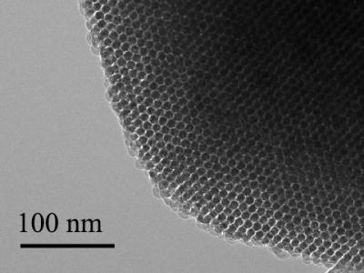
Finally, the mold is dissolved. What remains is a web-like structure of silicon nano-wires connected by micro-bridges of oxidized silicon that can absorb water and help increase the structure’s softness. The pure silicon retains its ability to absorb light.

Transmission electron microscopy image shows an ordered nanowire array. The 100-nanometer scale bar is 1,000 times narrower than a hair. Courtesy of Tian Lab

Transmission electron microscopy image shows an ordered nanowire array. The 100-nanometer scale bar is 1,000 times narrower than a hair. Courtesy of
Tian Lab

The scientists have added the particles onto neurons in culture in the lab, shone light on the particles, and seen current flow into the neurons which activates the cells. The next step is to see what happens in living animals. They are particularly interested in stimulating nerves in the peripheral nervous system that connect to organs. These nerves are relatively close to the surface of the body, so near-infra-red wavelength light can reach them through the skin.

Tian imagines using the light-activated devices to engineer human tissue and create artificial organs to replace damaged ones. Currently, scientists can make engineered organs with the correct form but not the ideal function.

To get a lab-built organ to function properly, they will need to be able to manipulate individual cells in the engineered tissue. The injectable device would allow a scientist to do that, tweaking an individual cell using a tightly focused beam of light like a mechanic reaching into an engine and turning a single bolt. The possibility of doing this kind of synthetic biology without genetic engineering [emphasis mine] is enticing.

“No one wants their genetics to be altered,” Tian said. “It can be risky. There’s a need for a non-genetic system that can still manipulate cell behavior. This could be that kind of system.”

Tian’s graduate student Yuanwen Jiang did the material development and characterization on the project. The biological part of the collaboration was done in the lab of Francisco Bezanilla, the Lillian Eichelberger Cannon Professor of Biochemistry and Molecular Biology, by postdoc João L. Carvalho-de-Souza. They were, said Tian, the “heroes” of the work.

I was a little puzzled about the use of the word ‘micro’ in a context suggesting it was smaller than something measured at the nanoscale. Dr. Tian very kindly cleared up my confusion with this response in a July 4, 2016 email,

In fact, the definition of ‘micro’ and ’nano’ have been quite ambiguous in literature. For example, microporous materials (e.g., zeolite) usually refer to materials with pore sizes of less than 2 nm — this is defined based on IUPAC [International Union of Pure and Applied Chemistry] definition (http://goldbook.iupac.org/M03853.html). We used ‘micro-bridges’ because they come from the ‘micropores’ in the original template.

Thank you Dr. Tian for that very clear reply and Steve Koppes for forwarding my request to Dr. Tian!

Here’s a link to and a citation for the paper,

Heterogeneous silicon mesostructures for lipid-supported bioelectric interfaces by Yuanwen Jiang, João L. Carvalho-de-Souza, Raymond C. S. Wong, Zhiqiang Luo, Dieter Isheim, Xiaobing Zuo, Alan W. Nicholls, Il Woong Jung, Jiping Yue, Di-Jia Liu, Yucai Wang, Vincent De Andrade, Xianghui Xiao, Luizetta Navrazhnykh, Dara E. Weiss, Xiaoyang Wu, David N. Seidman, Francisco Bezanilla, & Bozhi Tian. Nature Materials (2016)  doi:10.1038/nmat4673 Published online 27 June 2016

This paper is behind a paywall.

I gather animal testing will be the next step as they continue to develop this exciting technology. Good luck!

Gold nanoparticles and two different collective oscillations

An April 27, 2016 news item on phys.org describes research into gold nanoparticles and Surface Plasmon Resonance at Hokkaido University and the University of Tsukuba (Japan),

The research group of Professor Hiroaki Misawa of Research Institute for Electronic Science, Hokkaido University and Assistant Professor Atsushi Kubo of the Faculty of Pure and Applied Sciences, University of Tsukuba, have successfully observed the dephasing time of the two different types of collective motions of electrons generated on the surface of a gold nanoparticle for the first time in the world, by combining a laser that emits ultrashort light pulses with a photoemission electron microscope.

An April 26, 2016 Hokkaido University press release, which originated the news item, explains further,

When gold is reduced to the size in nanometer scale, its color is red instead of gold. When gold nanoparticles are exposed to light, the collective oscillations of electrons existing on the localized surface of the gold causes red light to be strongly absorbed and dispersed.

This phenomenon is called Surface Plasmon Resonance. The red color of stained glass is also a result of this phenomenon. Recently, gold nanoparticles have been widely used in various fields, such as application in pregnancy tests.

This collective oscillations of electrons on the surface of gold nanoparticles caused by light was considered to be a phenomenon that sustained only for an extremely short time, and difficult to measure due to this shortness.

Our research group developed a methodology to measure the dephasing time of the collective oscillations of electrons occurring on the surface of gold nanoparticles by combining a laser that emits ultrashort light pulses of a few femtoseconds (1 femtosecond: 1´10-15 seconds), and a photoemission electron microscope in high spatial resolution.

When measured by this technique, the different dephasing times of the two different collective oscillations, namely dipole and quadrupole surface plasmon modes, could be resolved and identified as 5 femtoseconds and 9 femtoseconds, respectively.

Research using gold nanoparticles as optical antennae to harvest light for photovoltaic cell and an artificial photosynthesis system that can split water to obtain hydrogen is progressing. The successful measurement of the dephasing time of the collective oscillations of electrons is considered to be a useful guideline in developing these systems.

Here’s a link to and a citation for the paper,

Dissecting the Few-Femtosecond Dephasing Time of Dipole and Quadrupole Modes in Gold Nanoparticles Using Polarized Photoemission Electron Microscopy by Quan Sun†, Han Yu, Kosei Ueno, Atsushi Kubo, Yasutaka Matsuo, and Hiroaki Misawa. ACS Nano, 2016, 10 (3), pp 3835–3842 DOI: 10.1021/acsnano.6b00715Publication Date (Web): February 15, 2016

Copyright © 2016 American Chemical Society

This paper appears to be open access.

Clothes washers and dryers begone! Nano-enhanced textiles can self-clean

It will be a while yet even it this technique proves to be viable commercially, still, the possibilities tantalize: self-cleaning textiles. A March 22, 2016 news item on ScienceDaily announced research in Australia that may, one day, change your life,

A spot of sunshine is all it could take to get your washing done, thanks to pioneering nano research into self-cleaning textiles.

Researchers at RMIT University in Melbourne, Australia, have developed a cheap and efficient new way to grow special nanostructures — which can degrade organic matter when exposed to light — directly onto textiles.

The work paves the way towards nano-enhanced textiles that can spontaneously clean themselves of stains and grime simply by being put under a light bulb or worn out in the sun.

A March 22, 2016 RMIT media release (also on EurekAlert), which originated the news item, expands on the theme,

Dr Rajesh Ramanathan said the process developed by the team had a variety of applications for catalysis-based industries such as agrochemicals, pharmaceuticals and natural products, and could be easily scaled up to industrial levels.

“The advantage of textiles is they already have a 3D structure so they are great at absorbing light, which in turn speeds up the process of degrading organic matter,” he said.

“There’s more work to do to before we can start throwing out our washing machines, but this advance lays a strong foundation for the future development of fully self-cleaning textiles.”

The researchers from the Ian Potter NanoBioSensing Facility and NanoBiotechnology Research Lab at RMIT worked with copper and silver-based nanostructures, which are known for their ability to absorb visible light.

When the nanostructures are exposed to light, they receive an energy boost that creates “hot electrons”. These “hot electrons” release a burst of energy [emphasis mine] that enables the nanostructures to degrade organic matter.

The challenge for researchers has been to bring the concept out of the lab by working out how to build these nanostructures on an industrial scale and permanently attach them to textiles.

The RMIT team’s novel approach was to grow the nanostructures directly onto the textiles by dipping them into a few solutions, resulting in the development of stable nanostructures within 30 minutes.

When exposed to light, it took less than six minutes for some of the nano-enhanced textiles to spontaneously clean themselves.

“Our next step will be to test our nano-enhanced textiles with organic compounds that could be more relevant to consumers, to see how quickly they can handle common stains like tomato sauce or wine,” Ramanathan said.

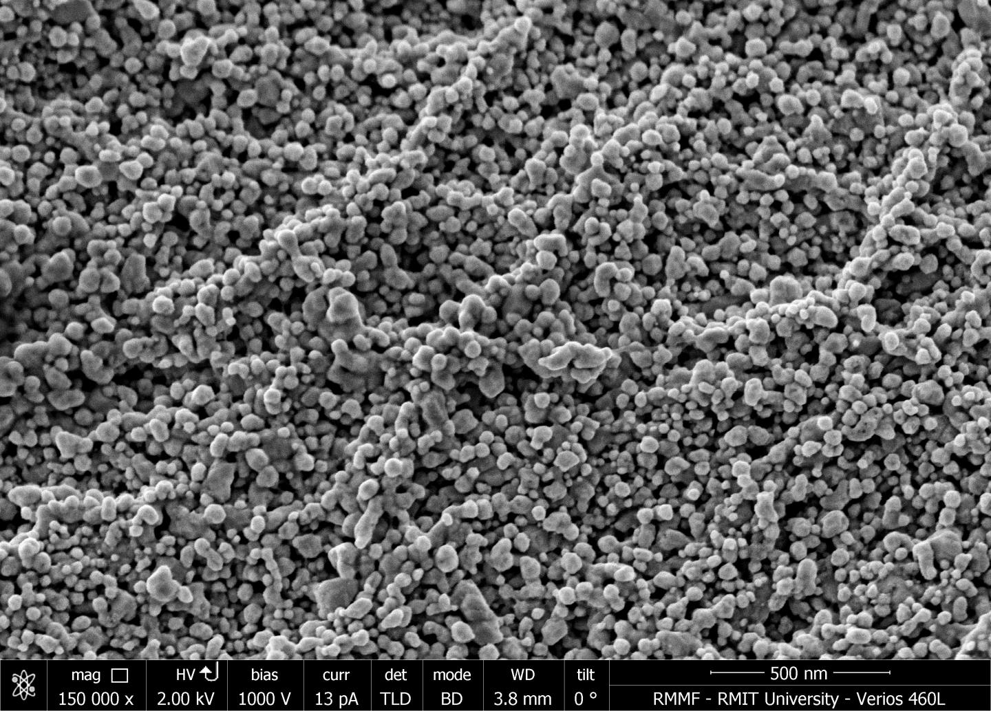
I wonder if these “hot electrons” mean that when they release “a burst of energy” your clothing will heat up when exposed to light? This image supplied by the researchers does not help to answer the question but it is intriguing,

Caption: Close-up of the nanostructures grown on cotton textiles by RMIT University researchers. Image magnified 150,000 times. Credit: RMIT University

Caption: Close-up of the nanostructures grown on cotton textiles by RMIT University researchers. Image magnified 150,000 times. Credit: RMIT University

Here’s a link to and a citation for the paper,

Robust Nanostructured Silver and Copper Fabrics with Localized Surface Plasmon Resonance Property for Effective Visible Light Induced Reductive Catalysis by Samuel R. Anderson, Mahsa Mohammadtaheri, Dipesh Kumar, Anthony P. O’Mullane, Matthew R. Field, Rajesh Ramanathan, and Vipul Bansal. Advanced Materials Interfaces DOI: 10.1002/admi.201500632 Article first published online: 7 JAN 2016

© 2016 WILEY-VCH Verlag GmbH & Co. KGaA, Weinheim

This paper is behind a paywall.
Explaining research into matching plasmonic nanoantenna resonances with atoms, molecules, and quantum dots

There’s a very nice explanation of the difficulties associeated with using plasmonic nanoantennas as sensors in a March 21, 2016 news item on phys.org,

Plasmonic nanoantennas are among the hot topics in science at the moment because of their ability to interact strongly with light, which for example makes them useful for different kinds of sensing. But matching their resonances with atoms, molecules or so called quantum dots has been difficult so far because of the very different length scales involved. Thanks to a grant from the Engkvist foundation, Timur Shegai, assistant professor at Chalmers University of Technology, hopes to find a way to do this and by that open doors for applications such as safe long distance communication channels.

A molecule being illuminated by two gold nanoantennas. By: Alexander Ericson Courtesy: Chalmers University of Technology

A molecule being illuminated by two gold nanoantennas. By: Alexander Ericson Courtesy: Chalmers University of Technology

The image, looking like a stylized butterfly or bow tie, above accompanies Karin Weijdegård’s March ??, 2016 Chalmers University of Technology press release, which originated the news item, expands on the research theme,

The diffraction limit makes it very hard for light to interact with the very smallest particles or so called quantum systems such as atoms, molecules or quantum dots. The size of such a particle is simply so much smaller than the wavelength of light that there cannot be a strong interaction between the two. But by using plasmonic nanoantennas, which can be described as metallic nanostructures that are able to focus light very strongly and in wavelengths smaller than those of the visible light, one can build a bridge between the light and the atom, molecule or quantum dot and that is what Timur Shegai is working on.

“Plasmonic nanostructures are themselves smaller than wavelengths of light, but because they have a lot of free electrons they can store the electromagnetic energy in a volume which is actually a lot smaller than the diffraction limit, which helps to bridge the gap between really small objects such as molecules and the larger wavelengths of light,” he says.

Matching the harmonic with the un-harmonic

This might sound easy enough, but the problem with combining the two is that they behave in very different ways. The behaviour of plasmonic nanostructures is very linear, like a harmonic oscillator it will regularly move from side to side no matter how much energy or in other words how many excitations are stored in it. On the other hand, so called quantum systems like atoms, molecules or quantum dots are very much the opposite – their optical properties are highly un-harmonic. Here it makes a big difference if you excite the system with one or two or hundreds of photons.

“Now imagine that you couple together this un-harmonic resonator and a harmonic resonator, and add the possibility to interact with light much stronger than the un-harmonic system alone would have allowed. That opens up very interesting possibilities for quantum technologies and for non-linear optics for example. But as opposed to previous attempts that have been done at very low temperatures and in a vacuum, we will do it at room temperature.”

Communication channels impossible to hack

One possible application where this technology could be useful in the future is to create channels for long distance communications that are impossible to hack. With the current technology this kind of safe communication is only possible if the persons communicating is within a distance of about one hundred kilometres from each other, because that is the maximum distance that an individual photon can run in fibres before it scatters and the signal is lost.

“The kind of ultra small and ultra fast technology we want to develop could be useful in a so called quantum repeater, a device that could be installed across the line from for example New York to London, that would repeat the photon every time it is about to be scattered,” says Timur Shegai.

At the moment though, it is the fundamental aspects of merging plasmons with quantum systems that interest Timur Shegai. To be able to experimentally prove that the there can be interactions between the two systems, he first of all needs to fabricate model systems at the nano level. This is a big challenge, but with the grant of 1,6 million SEK over a period of two years that he just received from the Engkvist foundation, the chances of success have improved.

“Since I am a researcher at the beginning of my career every person is a huge improvement and now I can hire a post doc to work with my group. This means that the project can be divided into sub parts and together we will be able to explore more possibilities about this new technology.”

Thank you Karin Weijdegård for the explanation.

Plasmonic interferometry without coherent light

There are already a number of biosensors based on plasmonic interferometry in use but this latest breakthrough from Brown University (US) could make them cheaper and more accessible. A Feb. 16, 2016 Brown University news release (also on EurekAlert), announces the new technique,

Imagine a hand-held environmental sensor that can instantly test water for lead, E. coli, and pesticides all at the same time, or a biosensor that can perform a complete blood workup from just a single drop. That’s the promise of nanoscale plasmonic interferometry, a technique that combines nanotechnology with plasmonics–the interaction between electrons in a metal and light.

Now researchers from Brown University’s School of Engineering have made an important fundamental advance that could make such devices more practical. The research team has developed a technique that eliminates the need for highly specialized external light sources that deliver coherent light, which the technique normally requires. The advance could enable more versatile and more compact devices.

“It has always been assumed that coherent light was necessary for plasmonic interferometry,” said Domenico Pacifici, a professor of engineering who oversaw the work with his postdoctoral researcher Dongfang Li, and graduate student Jing Feng. “But we were able to disprove that assumption.”

The research is described in Nature Scientific Reports.

Plasmonic interferometers make use of the interaction between light and surface plasmon polaritons, density waves created when light energy rattles free electrons in a metal. One type of interferometer looks like a bull’s-eye structure etched into a thin layer of metal. In the center is a hole poked through the metal layer with a diameter of about 300 nanometers–about 1,000 times smaller than the diameter of a human hair. The hole is encircled by a series of etched grooves, with diameters of a few micrometers. Thousands of these bulls-eyes can be placed on a chip the size of a fingernail.

When light from an external source is shown onto the surface of an interferometer, some of the photons go through the central hole, while others are scattered by the grooves. Those scattered photons generate surface plasmons that propagate through the metal inward toward the hole, where they interact with photons passing through the hole. That creates an interference pattern in the light emitted from the hole, which can be recorded by a detector beneath the metal surface.

When a liquid is deposited on top of an interferometer, the light and the surface plasmons propagate through that liquid before they interfere with each other. That alters the interference patterns picked up by the detector depending on the chemical makeup of the liquid or compounds present in it. By using different sizes of groove rings around the hole, the interferometers can be tuned to detect the signature of specific compounds or molecules. With the ability to put many differently tuned interferometers on one chip, engineers can hypothetically make a versatile detector.

Up to now, all plasmonic interferometers have required the use of highly specialized external light sources that can deliver coherent light–beams in which light waves are parallel, have the same wavelength, and travel in-phase (meaning the peaks and valleys of the waves are aligned). Without coherent light sources, the interferometers cannot produce usable interference patterns. Those kinds of light sources, however, tend to be bulky, expensive, and require careful alignment and periodic recalibration to obtain a reliable optical response.

But Pacifici and his group have come up with a way to eliminate the need for external coherent light. In the new method, fluorescent light-emitting atoms are integrated directly within the tiny hole in the center of the interferometer. An external light source is still necessary to excite the internal emitters, but it need not be a specialized coherent source.

“This is a whole new concept for optical interferometry,” Pacifici said, “an entirely new device.”

In this new device, incoherent light shown on the interferometer causes the fluorescent atoms inside the center hole to generate surface plasmons. Those plasmons propagate outward from the hole, bounce off the groove rings, and propagate back toward the hole after. Once a plasmon propagates back, it interacts with the atom that released it, causing an interference with the directly transmitted photon. Because the emission of a photon and the generation of a plasmon are indistinguishable, alternative paths originating from the same emitter, the process is naturally coherent and interference can therefore occur even though the emitters are excited incoherently.

“The important thing here is that this is a self-interference process,” Pacifici said. “It doesn’t matter that you’re using incoherent light to excite the emitters, you still get a coherent process.”

In addition to eliminating the need for specialized external light sources, the approach has several advantages, Pacifici said. Because the surface plasmons travel out from the hole and back again, they probe the sample on top of the interferometer surface twice. That makes the device more sensitive.

But that’s not the only advantage. In the new device, external light can be projected from underneath the metal surface containing the interferometers instead of from above. That eliminates the need for complex illumination architectures on top of the sensing surface, which could make for easier integration into compact devices.

The embedded light emitters also eliminate the need to control the amount of sample liquid deposited on the interferometer’s surface. Large droplets of liquid can cause lensing effects, a bending of light that can scramble the results from the interferometer. Most plasmonic sensors make use of tiny microfluidic channels to deliver a thin film of liquid to avoid lensing problems. But with internal light emitters excited from the bottom surface, the external light never comes in contact with the sample, so lensing effects are negated, as is the need for microfluidics.

Finally, the internal emitters produce a low intensity light. That’s good for probing delicate samples, such as proteins, than can be damaged by high-intensity light.

More work is required to get the system out of the lab and into devices, and Pacifici and his team plan to continue to refine the idea. The next step will be to try eliminating the external light source altogether. It might be possible, the researchers say, to eventually excite the internal emitters using tiny fiber optic lines, or perhaps electric current.

Still, this initial proof-of-concept is promising, Pacifici said.

“From a fundamental standpoint, we think this new device represents a significant step forward,” he said, “a first demonstration of plasmonic interferometry with incoherent light”.

Here’s a link to and a citation for the paper,

Nanoscale optical interferometry with incoherent light by Dongfang Li, Jing Feng, & Domenico Pacifici. Scientific Reports 6, Article number: 20836 (2016) doi:10.1038/srep20836 Published online: 16 February 2016

This paper is open access.

One final comment, Dexter Johnson has a Feb. 18, 2016 posting about this interferometer where he references Pacifici’s past work in this area, as well as, this latest breakthrough. Dexter’s posting can be found on his Nanoclast blog which is on the IEEE (Institute of Electrical and Electronics Engineers) website.

Constructing an autonomous Maxwell’s demon as a self-contained information-powered refrigerator

Aalto University (Finland) was the lead research institution for  INFERNOS, a European Union-funded project concerning Maxwell’s demon. Here’s an excerpt from an Oct. 14, 2013 post featuring the project,

An Oct. 9, 2013 news item on Nanowerk ties together INFERNOS and the ‘demon’,

Maxwell’s Demon is an imaginary creature that the mathematician James Clerk Maxwell created in 1897. The creature could turn heat into work without causing any other change, which violates the second law of thermodynamics. The primary goal of the European project INFERNOS (Information, fluctuations, and energy control in small systems) is to realize experimentally Maxwell’s Demon; in other words, to develop the electronic and biomolecular nanodevices that support this principle.

I like the INFERNOS logo, demon and all,

Logo of the European project INFERNOS (Information, fluctuations, and energy control in small systems).

A Jan. 11, 2016 news item on Nanowerk seems to be highlighting a paper resulting from the INFERNOS project (Note: A link has been removed),

On [a] theoretical level, the thought experiment has been an object of consideration for nearly 150 years, but testing it experimentally has been impossible until the last few years. Making use of nanotechnology, scientists from Aalto University have now succeeded in constructing an autonomous Maxwell’s demon that makes it possible to analyse the microscopic changes in thermodynamics. The research results were recently published in Physical Review Letters (“On-Chip Maxwell’s Demon as an Information-Powered Refrigerator”). The work is part of the forthcoming PhD thesis of MSc Jonne Koski at Aalto University.

An image illustrating the theory underlying the proposed device has been made available,

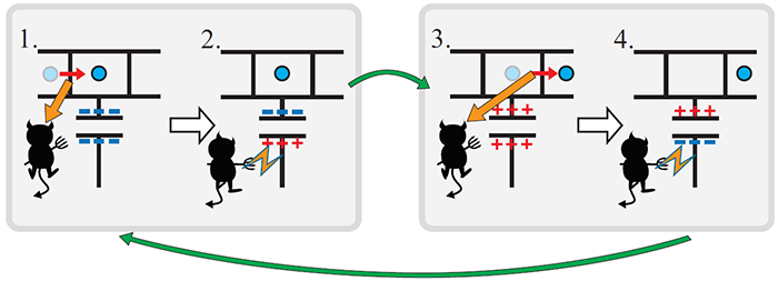
An autonomous Maxwell's demon. When the demon sees the electron enter the island (1.), it traps the electron with a positive charge (2.). When the electron leaves the island (3.), the demon switches back a negative charge (4.). Image: Jonne Koski.

An autonomous Maxwell’s demon. When the demon sees the electron enter the island (1.), it traps the electron with a positive charge (2.). When the electron leaves the island (3.), the demon switches back a negative charge (4.). Image: Jonne Koski.

A Jan. 11, 2016 Aalto University press release, which originated the news item, provides more technical details,

The system we constructed is a single-electron transistor that is formed by a small metallic island connected to two leads by tunnel junctions made of superconducting materials. The demon connected to the system is also a single-electron transistor that monitors the movement of electrons in the system. When an electron tunnels to the island, the demon traps it with a positive charge. Conversely, when an electron leaves the island, the demon repels it with a negative charge and forces it to move uphill contrary to its potential, which lowers the temperature of the system,’ explains Professor Jukka Pekola.

What makes the demon autonomous or self-contained is that it performs the measurement and feedback operation without outside help. Changes in temperature are indicative of correlation between the demon and the system, or, in simple terms, of how much the demon ‘knows’ about the system. According to Pekola, the research would not have been possible without the Low Temperature Laboratory conditions.

‘We work at extremely low temperatures, so the system is so well isolated that it is possible to register extremely small temperature changes,’ he says.

‘An electronic demon also enables a very large number of repetitions of the measurement and feedback operation in a very short time, whereas those who, elsewhere in the world, used molecules to construct their demons had to contend with not more than a few hundred repetitions.’

The work of the team led by Pekola remains, for the time being, basic research, but in the future, the results obtained may, among other things, pave the way towards reversible computing.

‘As we work with superconducting circuits, it is also possible for us to create qubits of quantum computers. Next, we would like to examine these same phenomena on the quantum level,’ Pekola reveals.

Here’s a link to and a citation for the paper,

On-Chip Maxwell’s Demon as an Information-Powered Refrigerator by J.V. Koski, A. Kutvonen, I.M. Khaymovich, T. Ala-Nissila, and J.P. Pekola. Phys. Rev. Lett. 115, 260602 DOI: http://dx.doi.org/10.1103/PhysRevLett.115.260602 Published 30 December 2015

This paper is behind a paywall.

One final comment, this is the 150th anniversary of Maxwell’s publication of a series of equations explaining the relationships between electric charges and electric and magnetic fields (featured here in a Nov. 27, 2015 posting).

The search for James Clerk Maxwell

The Brits really know how to celebrate an anniversary. In this case it’s the 150th anniversary of James Clerk Maxwell’s electromagnetic theory unifying electricity, magnetism, and light. (My Nov. 27, 2015 posting the first piece here featuring the anniversary and it describes the theory in more detail than you’ll find here.)

As part of the celebration there’s a five-episode series titled: Self Drives: Maxwell’s Equations being broadcast on BBC (British Broadcasting Corporation) 4. Stephen Curry writes about the series in a Dec. 9, 2015 posting on the Guardian science blogs (Note: Links have been removed),

There’s a potent antidote to the “Isn’t this amazing?” school of science communication and it’s called Will Self. In Self Drives: Maxwell’s Equations, which was broadcast recently [you can hear it as a podcast by visiting this site] on BBC Radio 4, the curious curmudgeon takes science to task once again as he goes in search of the mathematical and physical genius behind James Clerk Maxwell.

Over five short episodes, Self’s querulous quest takes him from Maxwell’s birthplace in Edinburgh to his family home in Glenlair, to the radio telescope at Jodrell Bank and the Diamond synchrotron near Oxford, and finally to Cambridge, where Maxwell studied mathematics in his youth and returned in his latter years as one of the nation’s most accomplished scientists to head the university’s Cavendish physics laboratory. Accompanying Self along the way is Akram Khan, the same physics professor who joined the errant writer on his earlier orbit of the Large Hadron Collider at CERN. I would have dubbed Khan Sancho Panza to Self’s Don Quixote but for this particular expedition the characters are reversed. It is Khan who wishes to see the poetry of science, while Self is happier to be grounded in prosaic and flawed reality. At CERN he refused truculently to worship in the cathedral of particle physics, stymied in equal measure by the difficulty of the subject matter and the boosterism of its scientific proponents. Here again the journey is mostly one of disappointment and frustration.

But not for the listener. The quest is far from fruitless, and nor is it lacking in emotional and intellectual force. Self’s documentary is not straight biography – you will find out more about Maxwell’s life and work from Wikipedia – but he has a different target in mind. …

Here’s the pair of explorers,

Will Self, Akram Khan and Maxwell’s infamous equations. Photograph: Laurence Grissell/BBC

Will Self, Akram Khan and Maxwell’s infamous equations. Photograph: Laurence Grissell/BBC

It’s good writing and an intriguing look into communicating science in a way that’s not quite so reverent and/or kid friendly as we tend to be in Canada.

‘Stained glass nanotechnology’ for color displays

From a Dec. 4, 2015 news item on ScienceDaily,

A new method for building “drawbridges” between metal nanoparticles may allow electronics makers to build full-color displays using light-scattering nanoparticles that are similar to the gold materials that medieval artisans used to create red stained-glass.

“Wouldn’t it be interesting if we could create stained-glass windows that changed colors at the flip of a switch?” said Christy Landes, associate professor of chemistry at Rice and the lead researcher on a new study about the drawbridge method that appears this week in the open-access journal Science Advances.

The research by Landes and other experts at Rice University’s Smalley-Curl Institute could allow engineers to use standard electrical switching techniques to construct color displays from pairs of nanoparticles that scatter different colors of light.

For centuries, stained-glass makers have tapped the light-scattering properties of tiny gold nanoparticles to produce glass with rich red tones. Similar types of materials could increasingly find use in modern electronics as manufacturers work to make smaller, faster and more energy-efficient components that operate at optical frequencies.

A Dec. 4, 2015 Rice University news release (also on EurekAlert), which originated the news item, describes the research in more detail,

Though metal nanoparticles scatter bright light, researchers have found it difficult to coax them to produce dramatically different colors, Landes said.

Rice’s new drawbridge method for color switching incorporates metal nanoparticles that absorb light energy and convert it into plasmons, waves of electrons that flow like a fluid across a particle’s surface. Each plasmon scatters and absorbs a characteristic frequency of light, and even minor changes in the wave-like sloshing of a plasmon shift that frequency. The greater the change in plasmonic frequency, the greater the difference between the colors observed.

“Engineers hoping to make a display from optically active nanoparticles need to be able to switch the color,” Landes said. “That type of switching has proven very difficult to achieve with nanoparticles. People have achieved moderate success using various plasmon-coupling schemes in particle assemblies. What we’ve shown though is variation of the coupling mechanism itself, which can be used to produce huge color changes both rapidly and reversibly.”

To demonstrate the method, Landes and study lead author Chad Byers, a graduate student in her lab, anchored pairs of gold nanoparticles to a glass surface covered with indium tin oxide (ITO), the same conductor that’s used in many smartphone screens. By sealing the particles in a chamber filled with a saltwater electrolyte and a silver electrode, Byers and Landes were able form a device with a complete circuit. They then showed they could apply a small voltage to the ITO to electroplate silver onto the surface of the gold particles. In that process, the particles were first coated with a thin layer of silver chloride. By later applying a negative voltage, the researchers caused a conductive silver “drawbridge” to form. Reversing the voltage caused the bridge to withdraw.

“The great thing about these chemical bridges is that we can create and eliminate them simply by applying or reversing a voltage,” Landes said. “This is the first method yet demonstrated to produce dramatic, reversible color changes for devices built from light-activated nanoparticles.”

This research has its roots in previous work (from the news release),

Byers said his research into the plasmonic behavior of gold dimers began about two years ago.

“We were pursuing the idea that we could make significant changes in optical properties of individual particles simply by altering charge density,” he said. “Theory predicts that colors can be changed just by adding or removing electrons, and we wanted to see if we could do that reversibly, simply by turning a voltage on or off.”

The experiments worked. The color shift was observed and reversible, but the change in the color was minute.

“It wasn’t going to get anybody excited about any sort of switchable display applications,” Landes said.

But she and Byers also noticed that their results differed from the theoretical predictions.

Landes said that was because the predictions were based upon using an inert electrode made of a metal like palladium that isn’t subject to oxidation. But silver is not inert. It reacts easily with oxygen in air or water to form a coat of unsightly silver oxide. This oxidizing layer can also form from silver chloride, and Landes said that is what was occurring when the silver counter electrode was used in Byers’ first experiments.

The scientists decided to embrace imperfection (from the news release),

“It was an imperfection that was throwing off our results, but rather than run away from it, we decided to use it to our advantage,” Landes said.

Rice plasmonics pioneer and study co-author Naomi Halas, director of the Smalley-Curl Institute, said the new research shows how plasmonic components could be used to produce electronically switchable color-displays.

“Gold nanoparticles are particularly attractive for display purposes,” said Halas, Rice’s Stanley C. Moore Professor of Electrical and Computer Engineering and professor of chemistry, bioengineering, physics and astronomy, and materials science and nanoengineering. “Depending upon their shape, they can produce a variety of specific colors. They are also extremely stable, and even though gold is expensive, very little is needed to produce an extremely bright color.”

In designing, testing and analyzing the follow-up experiments on dimers, Landes and Byers engaged with a brain trust of Rice plasmonics experts that included Halas, physicist and engineer Peter Nordlander, chemist Stephan Link, materials scientist Emilie Ringe and their students, as well as Paul Mulvaney of the University of Melbourne in Australia.

Together, the team confirmed the composition and spacing of the dimers and showed how metal drawbridges could be used to induce large color shifts based on voltage inputs.

Nordlander and Hui Zhang, the two theorists in the group, examined the device’s “plasmonic coupling,” the interacting dance that plasmons engage in when they are in close contact. For instance, plasmonic dimers are known to act as light-activated capacitors, and prior research has shown that connecting dimers with nanowire bridges brings about a new state of resonance known as a “charge-transfer plasmon,” which has its own distinct optical signature.

“The electrochemical bridging of the interparticle gap enables a fully reversible transition between two plasmonic coupling regimes, one capacitive and the other conductive,” Nordlander said. “The shift between these regimes is evident from the dynamic evolution of the charge transfer plasmon.”

Halas said the method provides plasmonic researchers with a valuable tool for precisely controlling the gaps between dimers and other multiparticle plasmonic configurations.

“In an applied sense, gap control is important for the development of active plasmonic devices like switches and modulators, but it is also an important tool for basic scientists who are conducting curiosity-driven research in the emerging field of quantum plasmonics.”

I’m glad the news release writer included the background work leading to this new research and to hint at the level of collaboration needed to achieve the scientists’ new understanding of color switching.

Here’s a link to and a citation for the paper,

From tunable core-shell nanoparticles to plasmonic drawbridges: Active control of nanoparticle optical properties by Chad P. Byers, Hui Zhang, Dayne F. Swearer, Mustafa Yorulmaz, Benjamin S. Hoener, Da Huang, Anneli Hoggard, Wei-Shun Chang, Paul Mulvaney, Emilie Ringe, Naomi J. Halas, Peter Nordlander, Stephan Link, and Christy F. Landes. Science Advances  04 Dec 2015: Vol. 1, no. 11, e1500988 DOI: 10.1126/sciadv.1500988

In case you missed it in the news release, this is an open access paper.

James Clerk Maxwell and his science mashup unified theories of magnetism, electricity, and optics

It’s the 150th anniversary for a series of equations electric charges and electric and magnetic fields that are still being explored. Jon Butterworth in a Nov. 22, 2015 posting on the Guardian science blog network explains (Note: A link has been removed),

The chances are that you are reading this article on some kind of electronic technology. You are definitely seeing it via visible light, unless you have a braille or audio converter. And it probably got to you via wifi or a mobile phone signal. All of those things are understood in terms of the relationships between electric charges and electric and magnetic fields summarised in Maxwell’s [James Clerk Maxwell] equations, published by the Royal Society in 1865, 150 years ago.

Verbally, the equations can be summarised as something like:

Electric and magnetic fields make electric charges move. Electric charges cause electric fields, but there are no magnetic charges. Changes in magnetic fields cause electric fields, and vice versa.

The equations specify precisely how it all happens, but that is the gist of it.

Butterworth got a rare opportunity to see the original manuscript,

 Original manuscript of Maxwell’s seminal paper Photograph: Jon Butterworth/Royal Society [downloaded from http://www.theguardian.com/science/life-and-physics/2015/nov/22/maxwells-equations-150-years-of-light]

Original manuscript of Maxwell’s seminal paper Photograph: Jon Butterworth/Royal Society [downloaded from http://www.theguardian.com/science/life-and-physics/2015/nov/22/maxwells-equations-150-years-of-light]

I love this description from Butterworth,

It was submitted in 1864 but, in a situation familiar to scientists everywhere, was held up in peer review. There’s a letter, dated March 1865, from William Thomson (later Lord Kelvin) saying he was sorry for being slow, that he’d read most of it and it seemed pretty good (“decidely suitable for publication”).

Then, there’s this,

The equations seem to have been very much a bottom-up affair, in that Maxwell collected together a number of known laws which were used to describe various experimental results, and (with a little extra ingredient of his own) fitted them into a unified framework. What is amazing is how much that framework then reveals, both in terms of deep physical principles, and rich physical phenomena.

I’m not excerpting any part of Butterworth’s description of how Maxwell fit these equations together for his unification theory as I think it should be read in its totality.

The section on quantum mechanics is surprising,

Now, one thing Maxwell’s equations don’t contain is quantum mechanics [emphasis mine]. They are classical equations. But if you take the quantum mechnical description of an electron, and you enforce the same charge conservation law/voltage symmetry that was contained in the classical Maxwell’s equations, something marvellous happens [emphasis mine]. The symmetry is denoted “U(1)”, and if you enforce it locally – that it, you say that you have to be allowed make different U(1) type changes to electrons at different points in space, you actually generate the quantum mechanical version of Maxwell’s equations out of nowhere [emphasis mine]. You produce the equations that describe the photon, and the whole of quantum electrodynamics.

I encourage you to read Butterworth’s Nov. 22, 2015 posting where he also mention two related art/science projects and has embedded a video animation of the principles discussed in his posting.

For anyone unfamiliar with Butterworth, there’s this description at the Guardian,

Jon Butterworth is a physics professor at University College London. He is a member of the UCL High Energy Physics group and works on the Atlas experiment at Cern’s Large Hadron Collider. His book Smashing Physics: The Inside Story of the Hunt for the Higgs was published in May 2014